Abstract
We present a detailed atomic-level study of defects in bilayer MoS2 using aberration-corrected transmission electron microscopy at an 80 kV accelerating voltage. Sulfur vacancies are found in both the top and bottom layers in 2H- and 3R-stacked MoS2 bilayers. In 3R-stacked bilayers, sulfur vacancies can migrate between layers but more preferably reside in the (Mo–2S) column rather than the (2S) column, indicating more complex vacancy production and migration in the bilayer system. As the point vacancy number increases, aggregation into larger defect structures occurs, and this impacts the interlayer stacking. Competition between compression in one layer from the loss of S atoms and the van der Waals interlayer force causes much less structural deformations than those in the monolayer system. Sulfur vacancy lines neighboring in top and bottom layers introduce less strain compared to those staggered in the same layer. These results show how defect structures in multilayered two-dimensional materials differ from their monolayer form.
Introduction
Transition metal dichalcogenides (TMDs), such as MoS2 and WS2, are direct band gap semiconductors in their monolayer form and indirect band gap semiconductors in bulk.1−4 They offer band gaps in the red visible spectrum and semiconducting properties that expand the application of two-dimensional (2D) materials beyond what graphene alone can achieve.5−7 The presence of defects in TMDs influences the photoluminescence spectra, electron transport behavior, and photosensing capabilities.8−12 Understanding the structure of the defects is important for developing an accurate picture of their impact on properties. Aberration-corrected transmission electron microscopy (AC-TEM) is one of the leading approaches to study the atomic structure of defects in 2D materials.13
With the availability of monolayer TMDs, detailed atomic-level studies of vacancies in MoS2 and other S- and Se-based TMDs have been performed.14−24 However, no detailed studies on the structure and dynamics of defects in bilayer TMDs have been reported. MoS2 or WS2 bilayers have two natural stacking forms: 3R and 2H stacking, with 2H dominating due to energetic preference.25,26 Most recent work has been focused on the 2H stacking structure and related optical properties27 and some has been performed on 3R-stacked MoS2 due to its relative rarity.28
Upon 80 kV electron beam irradiation of MoS2 and WS2, S vacancies are created and also mobilized, resulting in point defects that combine to form line defects.14,29−32 The line defects in MoS2 can extend in length and also in width. As the length of a one sulfur vacancy line (1SVL) defect increases, large lattice compression occurs to accommodate the loss of S atoms and change in charge density around the Mo atoms. This also causes large out-of-plane distortion to the monolayer sheet, similar to the buckling in graphene monolayers caused by dislocations.33 The ability of monolayer sheets to buckle when defects are introduced plays an important role in strain relief.34 Recent work has shown that heating graphene to high temperatures causes the substrate it is attached to expand and produce tension on graphene.35 This in turn causes partial dislocations to occur because single dislocation cores are only stable when accompanied by out-of-plane buckling. The ability of a 2D material to accommodate buckling and defects is expected to be different as more layers are added, due to the interlayer van der Waals forces. Unique interlayer interactions have been previously seen in bilayer graphene, with very small mismatch angles between the layers, causing local regions of commensurate and incommensurate stacking.36 Recent work has shown that as the width of line vacancies in MoS2 increases, the rows of S vacancy lines are staggered from top to bottom to enable stable bond restructuring.12 The reconstructed bonds have different unit cell structures, and this will cause changes in the local van der Waals interactions with the second layer in bilayer 2D systems. Furthermore, the compression associated with the multiple stacked line vacancies in MoS2 will cause local shifts in atomic positions extending out from the defect region, and this will give rise to competition between in-plane compression around defects and interlayer van der Waals forces and associated 2H and 3R stacking phases.
In this study, MoS2 samples are grown on Si substrates with a 300 nm oxide layer using methods based on our prior work.12 Samples of MoS2 are predominantly monolayers, but sometimes, small bilayer domains are found. We study the structure and dynamics of defects in bilayer MoS2, from point defects to aggregated clusters. Both 2H- and 3R-stacked bilayers are examined due to their presence in chemical vapor deposition (CVD)-grown samples. Density functional theory (DFT) calculations are used to provide accurate model structures for multislice image simulations to compare to the experimental phase contrast AC-TEM images.
Results and Discussion
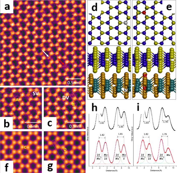
For our as-grown monolayer and few-layer MoS2 (as indicated in Figure S1), the interface of the monolayer and 2H-stacked bilayer MoS2 are shown in Figure S2a,b. First, we examine the presence of S vacancies in the 2H-stacked bilayer MoS2 (Figure 1). Electron beam irradiation at 80 kV is known to introduce sulfur vacancies in MoS2.13Figure 1a shows a typical AC-TEM image of a 2H-stacked bilayer, with visible weaker contrast spots marked by white and red arrows. The magnified images in Figure 1b,c show two different levels of reduced contrast associated with single S vacancies (SVs) and double S vacancies (DVs) in the same column. Atomic models of 1SV (gray) and 1DV (red) from DFT calculations are respectively shown in Figure 1d,e in both top (colored ball) and three-dimensional (3D) views (colored cross). Corresponding multislice image simulations (Figure 1f,g) and line profile analysis (Figure 1h,i) show good similarity with the experimental results, confirming SVs and DVs in 2H-stacked bilayer MoS2.
Figure 1.
(a) AC-TEM image of SVs and DVs in 2H-stacked bilayer MoS2, marked by white and red arrows, respectively. Zoomed in high-resolution transmission electron microscopy (HRTEM) image indicating (b) SVs and (c) DVs. (f, g) Multislice image simulations based on DFT-calculated atomic models with (d) one missing S atom and (e) two missing S atoms in the Mo–S–S column, respectively. The color key is SV = gray, DV = red. (h) Boxed line profiles of the SVs shown in (b) and (f). (i) Boxed line profiles of the DVs shown in (c) and (g).
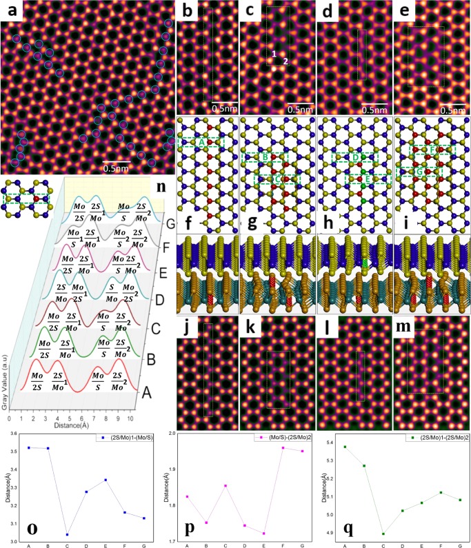
Under prolonged electron beam irradiation, SVs and DVs in 2H bilayer MoS2 increase in density and start to aggregate into extended line defects, as shown in Figure 2a. The line defects in 2H bilayer MoS2 can exist in variable lengths along the zigzag directions and also gain width along the armchair direction (Figure 2b–e). The magnified AC-TEM image in Figure 2b shows a 1SVL, with a length of 7SVs. The corresponding DFT-calculated model, in top and 3D views (Figure 2f), shows negligible in-plane or out-of-plane lattice distortions, triggered by losing seven S atoms in the bottom layer, which differs from the findings of prior studies on 1SVLs in monolayer MoS2.13 Two types of 2SVLs are observed (Figure 2c,d), with different S reconstructions. Two corresponding DFT-calculated models are evaluated (Figure 2g,h). Type A has 2SVLs within only one MoS2 layer, with alternate staggering across top and bottom S sites. On the basis of a previous report,12 the staggering configuration of two vacancy lines in the bottom layer is energetically preferred. Type B has one 1SVL in the bottom and the other in the top MoS2 layer, giving a 2SVL defect overall, spread across the two layers. The vacancy lines can exist in either plane of each layer. DFT calculations indicate that no obvious out-of-plane distortion occurs in either type A or B 2SVLs in the 2H bilayer, which is different from that in the 2SVL in monolayer MoS2. The observation of type B 2SVL also indicates the coexistence of S vacancies in both the bottom and top layers in the 2H-stacked MoS2 bilayer. In Figure 2e, a 3SVL is presented, showing a similar structure to that of A-2SVL. The atomic model relaxed using DFT calculations (Figure 2i) shows a staggered arrangement of SVLs in the bottom layer.
Figure 2.
(a) AC-TEM image showing the aggregation of S vacancies into extended line defects along a zigzag direction with different lengths and widths. HRTEM images showing (b) 1SVL, (c) type A-2SVL, (d) type B-2SVL, and (e) 3SVL, with the defective region in a yellow dashed rectangle, and (f–i) corresponding DFT-calculated atomic models. The S vacancies are marked in red in the bottom and green in the top layer (colored balls in the top view and colored crosses in the 3D view). (j–m) Multislice image simulations based on (f)–(i). (n) Boxed line profiles taken along green dashed rectangles marked as A–G. Scattered line graphs displaying the distance between (o) (2S/Mo)1 and (Mo/S), (p) (Mo/S) and (2S/Mo)2, and (q) (2S/Mo)1 and (2S/Mo)2.
To quantify the lattice distortion introduced by each SVL in 2H bilayer MoS2 (Figure 2n), we measured the boxed line profiles across (Mo/2S)–(2S/Mo)1–(Mo/S)–(2S/Mo)2 columns, as marked by green dashed rectangles for 1SVL (A), A-2SVL (B and C), B-2SVL (D and E), and 3SVL (F and G). The distance between each column is determined by fitting Gaussian curves and plotted for A–G in Figure 2o–q. For 1SVL, the (2S/Mo)1–(Mo/S), (Mo/S)–(2S/Mo)2, and (2S/Mo)1–(2S/Mo)2 distances are 3.52, 1.83, and 5.38 Å, respectively. The negligible shrinkage compared to the column distances in pristine 2H bilayer MoS2 confirms minimal compression in the system when losing seven S atoms in a layer. The line profiles along directions B and C, the left-side SVL in A-2SVL, show no (2S/Mo)1–(Mo/S) distance change but a slight drop in the (Mo/S)–(2S/Mo)2 and (2S/Mo)1–(2S/Mo)2 distances. However, for the right-side SVL, the (2S/Mo)1–(Mo/S) and (2S/Mo)1–(2S/Mo)2 distances shrink to 3.04 and 4.90 Å, with a small increase in the (2S/Mo)1–(Mo/S) distance. These changes indicate greater compression introduced between the two staggered SVLs. For the right-side SVL, the (2S/Mo)1–(Mo/S) distance increment, indicating tension, is caused by the displacement of S atoms in (Mo/S) toward the (2S/Mo) column. The directions D and E in B-2SVL both show compression along the armchair direction. Compared to those in A-2SVL, no tension exists in the defective regions and the contraction is relatively smaller, indicating that the configuration having one sulfur vacancy line in each layer introduces less strain into the bilayer system. The staggered 3SVL shows expansion of the (Mo/S)–(2S/Mo)2 distance and shrinkage of the (2S/Mo)1–(2S/Mo)2 distance, as expected.
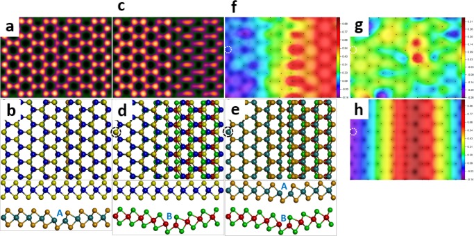
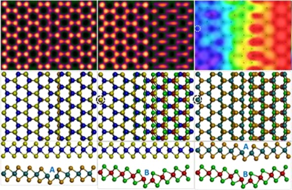
Figure 3a shows a multislice image simulation of 2H-stacked bilayer MoS2 with an infinitely long 1SVL running through the bottom layer on the DFT-calculated atomic model in Figure 3b. As discussed before, the introduction of 1SVL introduces negligible out-of-plane and in-plane lattice distortions. To compare the difference between the SVLs in the monolayer and bilayer system, as shown in Figure 3d, layer B is DFT-calculated model for monolayer MoS2 with 1SVL running through, another pristine MoS2 monolayer is manually placed on top to create similar 2H stacking configuration, taking the circled column as the alignment point. The corresponding multislice image simulation in Figure 3c shows considerable lattice distortion on the right-hand side of the 1SVL, resulting from the mismatch between two layers. Layers A and B are then extracted and stacked, as shown in Figure 3e; the column circled in black is chosen as the alignment point. From the side view, a large discrepancy in the out-of-plane distortion between layers A and B can be distinguished. To quantify the lattice mismatch in the system, 2D displacement maps from the x, y, and z axes are constructed in Figure 3f–h, respectively. The reference point is circled in white. The displacement maps show significant compression with increased magnitude in the x direction. However, the lattice mismatch in the y direction is uniformly distributed and relatively small. The displacement map in the Z axis shows a centrosymmetric configuration, with most significant Z-direction distortion in the defective site and lowest, in the reference point, further confirming a large out-of-plane distortion difference between the two layers. We further measure the bond length of Mo–S in the defective site (shown in Figure S5). Compared to the value of 2.41 in pristine MoS2, the maximum bond length deviation for layers A and B is, respectively, 3.7 and 6.6%, indicating that the compression in the x direction also mainly comes from the out-of-plane distortion. Therefore, SVLs in the monolayer system introduce slightly larger in-plane lattice deformations than those in their bilayer counterparts. However, the main discrepancy between the defective layer in monolayer and bilayer systems is the out-of-plane distortion. The considerable buckling introduced by SVLs in monolayer MoS2 becomes insignificant in bilayer system, mainly compensated by the interlayer van der Waals force.
Figure 3.
Multislice image simulations of (a) bilayer MoS2 with 1SVL in layer A and (c) one pristine monolayer on top of one defective layer B and (b, d) corresponding DFT-calculated atomic models. (e) Atomic model of “bilayer” composed by layers A and B. Two-dimensional displacement maps along (f) x, (g) y, and (h) z directions, respectively, which are laid on top of a simulated image based on (e). Alignment points are marked with black circles in the image simulations, and reference points are marked with white circles in displacement maps.
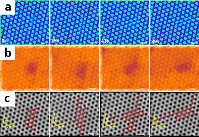
The sequential AC-TEM images in Figure 4a show the dynamics of S vacancies in 2H-stacked bilayer MoS2 during 89 s of electron beam irradiation. A different false color look up table (LUT) is applied to highlight every SV in each frame (Figure 4b). In Figure 4c, the gray scale image with red dots indicating SVs shows that during the first 25 s the 3SVL gains length in the B-zigzag direction. Vacancies initially aggregate along the A-zigzag direction from 25 to 43 s. Over the latter 46 s, a large number of vacancies along the B-zigzag direction are quenched and the SVL transforms to 3SVL along the A-zigzag direction. In the first 43 s, newly ejected S atoms adjacent to the 3SVL are introduced under electron beam irradiation. In the next 46 s, vacancies along the B-zigzag direction get quenched by free S atoms or migrate in the A-zigzag direction.
Figure 4.
(a) Series of processed AC-TEM images showing the evolution of S vacancies in 2H bilayer MoS2 over 89 s (a false color LUT is used to highlight vacancies). (b) S vacancies highlighted as darker spots using different false color LUTs. (c) Gray scale image showing vacancy migration and 3SVL rotation from the B-zigzag to the A-zigzag direction (S vacancies are marked as red dots).
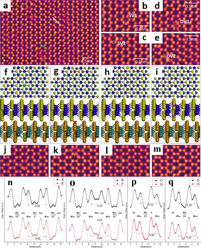
A monolayer–3R-stacked bilayer interface has also been observed in our study (Figure S2c,d). Figure 5a shows a typical AC-TEM image of 3R-stacked bilayer MoS2, in which a large number of bright spots (marked by white and purple arrows) and blurred regions (marked by green and red arrows) are observed. Magnified AC-TEM images in Figure 5b–e indicate SVs (SV1 and SV2) and DVs (DV1 and DV2) as blurred regions, bright spots, heavily blurred regions, and brighter spots, respectively. The existence of 3R-stacked bilayer MoS2 is confirmed by imaging the structure under different defocus values, leading to contrast pattern variations that the 2H structure cannot exhibit. The corresponding multislice image simulations under different defocus values match the experimental results (Figure S4). Atomic models relaxed by DFT (Figure 5f–i) and their corresponding multislice image simulations (Figure 5j–m) indicate that the blurriness is due to losing one (SV1) or two (DV1) S atoms in a 2S/Mo column and that the bright contrast is due to losing one (SV2) or two (DV2) S atoms in a 2S column. Intensity line profiles along the yellow arrows in both simulated and experimental images are taken covering the defective site. For both SVs (SV1 and SV2), the Mo–Mo column distance remains close to that in pristine 3R bilayer MoS2 (5.4 Å), implying that nearly no compression is introduced to the bilayer by losing one S atom. In contrast, a column distance shrinkage of ∼5% is observed for both DV1 and DV2, indicating small contraction caused by losing both S atoms in 2S or Mo/2S columns. These results are consistent with those on the SVs/DVs in 2H bilayer MoS2. Further confirmation of the existence of SVs/DVs in 3R-stacked bilayer MoS2 is obtained by measuring the peak intensity ratio at multiple defective sites, as shown in Figures 5n–q and S3.
Figure 5.
(a) AC-TEM image showing the distribution of S vacancies in 3R-stacked bilayer MoS2. The color key is SV1 = green, DV1 = red, SV2 = gray, DV2 = purple. Zoomed in HRTEM image indicating (b) SV1, (c) SV2, (d) DV1, and (e) DV2. (j–m) Multislice image simulations based on DFT-calculated atomic models of a 3R-stacked MoS2 bilayer with (f) one missing S atom and (g) two missing S atoms in the Mo-S–S column and (h) one missing S atom and (i) two missing S atoms in the S–S column, respectively. Vacancies are marked as colored balls in the top view and crosses in the 3D view. (n–q) Boxed line profiles taken along the yellow dashed rectangles marked A–H.
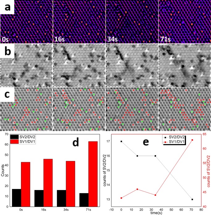
Processed AC-TEM images in Figure 6a,b highlight SV2/DV2 and SV1/DV1 as bright spots and dark regions, respectively. Figure 6c demonstrates the evolution of SV2/DV2 (green) and SV1/DV1 (red) under electron beam irradiation. The number of each SV is calculated as a function of time, as displayed in the histogram (Figure 6d) and plot (Figure 6e). Throughout the frames, the ratio of SV1/DV1 to SV2/DV2 increases from 2.5:1 to 4.9:1, indicating the dominance of SV1/DV1. Therefore, for 3R-stacked bilayer MoS2, under 80 kV irradiation, the S atoms in the 2S columns are more stable and less likely to be sputtered compared to those in the Mo/2S columns. Over 71 s, the SV2/DV2 number drops slightly, whereas the density of SV1/DV1 increases, especially in the last 37 s. Hence, the most newly produced SV1/DV1 are derived from the prolonged irradiation. However, vacancy migration also happen from SV2/DV2 to SV1/DV1, implying vacancy migration between layers in 3R bilayer MoS2.
Figure 6.
Processed AC-TEM images showing the evolution of (a) SV2/DV2 as bright spots and (b) SV1/DV1 as dimmed regions over 71 s. (c) Distribution of SV1/DV1 and SV2/DV2 marked as red and green spots, respectively. (d) Histogram and (e) trend lines representing the number change of SV1/DV1 and SV2/DV2 as a function of time.
Conclusions
AC-TEM imaging is conducted under an accelerating voltage of 80 kV, allowing production and aggregation of vacancies as well as atomic-level resolution of defective regions in bilayer MoS2. DFT-calculated models prove the different production and migration mechanisms between sulfur vacancies in monolayer and bilayer systems. The combination of DFT calculations and dislocation maps reveal that the main discrepancy between defective monolayer and bilayer systems is the out-of-plane lattice distortions. The ability for the bilayer sheet to accommodate the buckling and compression caused by line defects can be assigned to the competition between compression in one layer from the loss of S atoms and the interlayer van der Waals force.
Methods
MoS2 CVD Synthesis and Transfer
The synthesis of MoS2 was executed in two individually controlled quartz tube furnaces with only Ar flowing at atmospheric pressure using S powder (1 g of purum grade >99.5%) and MoO3 powder. The MoO3 precursor was initially loaded in a 1 cm diameter tube, which was in turn placed inside a larger diameter (1 in.) tube of the CVD furnace. This was to prevent cross-contamination of S and MoO3 prior to MoS2 formation on the target substrate, with the S kept separate in the larger diameter outer tube. Two furnaces were used to control the temperature of each precursor and the substrate, with heating temperatures of S at 180 °C, MoO3 at 300 °C, and the substrate at 800 °C. Ar was used as a carrier gas. The S was left to vaporize for an initial 15 min before the temperature of the second furnace was increased to 800 °C at 40 °C min–1 and left for 15 min under an Ar flow of 150 sccm. The Ar flow was then reduced to 10 sccm for 25 min, followed by a fast cooling process (sample removal). The S temperature was kept at 180 °C throughout.
The as-grown sample was first spin-coated with a poly(methyl methacrylate) (PMMA) scaffold (8 wt % in anisole, 495k molecular weight) at 4700 rpm for 60 s and then cured at 150 °C for 15 min. The edge of the wafer was ground with a diamond file to expose the SiO2/Si edges to the etchant solution. The underlying SiO2/Si substrate was subsequently detached by floating the sample on a 15 M KOH (Sigma-Aldrich) solution in a water bath for 2 h at 40 °C. The suspended PMMA–MoS2 film was thoroughly cleaned by transferring and floating onto fresh deionized water several times. For the TEM characterization, the PMMA–MoS2 film was transferred onto a holey Quantifoil TEM grid and left to dry overnight in air. PMMA–MoS2–Quantifoil was subsequently baked at 150 °C for 15 min to improve sample adhesion. The sample was eventually prepared by removing PMMA using an 8 h acetone solution bath.
Electron Microscopy
AC-TEM was performed at an accelerating voltage of 80 kV using Oxford’s JEOL 2200MCO, with an imaging CEOS corrector. The beam current density under imaging conditions was ∼105 e nm–2 s–1, with typical exposure times of 1–3 s.
Image Simulations and Processing
Multislice image simulations were conducted using JEMS software with an 80 kV accelerating voltage, 5 nm defocus spread, 3 nm (for 2H stacking) or 9 nm (for 3R stacking) defocus value, and 5 μm Cs. To match the AC-TEM image in Figure S2d, the simulation in Figure S2h was performed using 1.6 nm twofold astigmatism and 300 nm second-order coma (180°). The brightness and contrast of the simulated images were adjusted according to the intensity of the known columns in the experimental images, such as the (2S/Mo), (2S), and (S/Mo) columns.
ImageJ was used to process the AC-TEM images. A bandpass filter (between 100 and 1 pixels) and a Gaussian blur were carefully applied to minimize long-range uneven illumination without affecting the interpretation of the original image. Figure 4b was processed by an 8 pixel Gaussian blur, followed by a “find edge” filter, then another 8 pixel Gaussian blur, and then using an “orange hot”-colored LUT, and finally, the contrast and brightness were adjusted. In Figure 6a, bright SVs in bilayer 3R-stacked MoS2 were processed by fast Fourier transform (FFT) band pass (100-1 pixels) and then a Gaussian blur of 12 pixels, followed by contrast adjustment. Dark S vacancies, as shown in Figure 6b, were processed by an FFT band pass filter (100-1 pixels), then a Gaussian blur of 8 pixels, followed by a find edge filter, and then another 6 pixel Gaussian blur, and then, the contrast was adjusted.
DFT Calculation
Standard ab initio simulations within the DFT were performed, using the Vienna ab initio simulation package (VASP v5.4),37 to explore the atomic structures of 2D MoS2 bilayers with various defects in the 2H and 3R stacking configurations. Plane-wave and projector-augmented-wave type pseudopotentials were adopted,38 with kinetic-energy cutoffs of up to 300 eV and the generalized gradient approximation-Perdew–Burke–Ernzerhof exchange-correlation functional.39 The DFT-D2 method of Grimme was implemented to account for the Van der Waals interactions,40 with a 50 Å cutoff radius for pair interactions. To eliminate artificial interactions between periodic images, a 20 Å vacuum was constructed in the direction perpendicular to that of the sheets. The initial structures were generated on the basis of the TEM images and relaxed until all forces were smaller than 0.02 eV Å–1. The Γ point was used for geometric optimization of S vacancies and finite line defects, whereas a Monkhorst–Pack k-point grid41 of 9 × 1 × 1 was employed in relaxation of infinite line defects.
Acknowledgments
J.H.W. is grateful for the support from the Royal Society. C.G. is grateful for the support from the Clarendon Fund.
Supporting Information Available
The Supporting Information is available free of charge on the ACS Publications website at DOI: 10.1021/acsomega.7b00734.
Optical and SEM images of monolayer and bilayer regions in MoS2; AC-TEM images of monolayer–bilayer interfaces in 2H and 3R MoS2 bilayers; additional images of S vacancies in 2H and 3R bilayer MoS2; AC-TEM images of 3R-stacked MoS2 under different focusing conditions; bond length measurements for defective monolayer and defective layer from the bilayer (PDF)
The authors declare no competing financial interest.
Supplementary Material
References
- Gong Y.; Lin J.; Wang X.; Shi G.; Lei S.; Lin Z.; Zou X.; Ye G.; Vajtai R.; Yakobson B. I.; et al. Vertical and in-Plane Heterostructures from WS2/MoS2 Monolayers. Nat. Mater. 2014, 13, 1135–1142. 10.1038/nmat4091. [DOI] [PubMed] [Google Scholar]
- Plechinger G.; Nagler P.; Kraus J.; Paradiso N.; Strunk C.; Schüller C.; Korn T. Identification of excitons, trions and biexcitons in single-layer WS2. Phys. Status Solidi RRL 2015, 9, 457–461. 10.1002/pssr.201510224. [DOI] [Google Scholar]
- Withers F.; Bointon T. H.; Hudson D. C.; Craciun M. F.; Russo S. Electron Transport of WS2 Transistors in a Hexagonal Boron Nitride Dielectric Environment. Sci. Rep. 2014, 4, 4967 10.1038/srep04967. [DOI] [Google Scholar]
- Sorkin V.; Pan H.; Shi H.; Quek S. Y.; Zhang Y. W. Nanoscale Transition Metal Dichalcogenides: Structures, Properties, and Applications. Crit. Rev. Solid State Mater. Sci. 2014, 39, 319–367. 10.1080/10408436.2013.863176. [DOI] [Google Scholar]
- Komsa H.-P.; Kotakoski J.; Kurasch S.; Lehtinen O.; Kaiser U.; Krasheninnikov A. V. Two-Dimensional Transition Metal Dichalcogenides under Electron Irradiation: Defect Production and Doping. Phys. Rev. Lett. 2012, 109, 035503 10.1103/PhysRevLett.109.035503. [DOI] [PubMed] [Google Scholar]
- Wang Q. H.; Kalantar-Zadeh K.; Kis A.; Coleman J. N.; Strano M. S. Electronics and Optoelectronics of Two-Dimensional Transition Metal Dichalcogenides. Nat. Nanotechnol. 2012, 7, 699–712. 10.1038/nnano.2012.193. [DOI] [PubMed] [Google Scholar]
- Ma Y.; Dai Y.; Guo M.; Niu C.; Lu J.; Huang B. Electronic and Magnetic Properties of Perfect, Vacancy-Doped, and Nonmetal Adsorbed MoSe2, MoTe2 and WS2 Monolayers. Phys. Chem. Chem. Phys. 2011, 13, 15546–15553. 10.1039/c1cp21159e. [DOI] [PubMed] [Google Scholar]
- K C S.; Longo R. C.; Addou R.; Wallace R. M.; Cho K. Impact of Intrinsic Atomic Defects on the Electronic Structure of MoS2 Monolayers. Nanotechnology 2014, 25, 375703 10.1088/0957-4484/25/37/375703. [DOI] [PubMed] [Google Scholar]
- Lin Y.-C.; Björkman T.; Komsa H.-P.; Teng P.-Y.; Yeh C.-H.; Huang F.-S.; Lin K.-H.; Jadczak J.; Huang Y.-S.; Chiu P.-W.; et al. Three-Fold Rotational Defects in Two-Dimensional Transition Metal Dichalcogenides. Nat. Commun. 2015, 6, 6736 10.1038/ncomms7736. [DOI] [PMC free article] [PubMed] [Google Scholar]
- Zhou W.; Zou X.; Najmaei S.; Liu Z.; Shi Y.; Kong J.; Lou J.; Ajayan P. M.; Yakobson B. I.; Idrobo J. C. Intrinsic Structural Defects in Monolayer Molybdenum Disulfide. Nano Lett. 2013, 13, 2615–2622. 10.1021/nl4007479. [DOI] [PubMed] [Google Scholar]
- Han Y.; Hu T.; Li R.; Zhou J.; Dong J. Stabilities and Electronic Properties of Monolayer MoS2 with One or Two Sulfur Line Vacancy Defects. Phys. Chem. Chem. Phys. 2015, 17, 3813–3819. 10.1039/C4CP04319G. [DOI] [PubMed] [Google Scholar]
- Wang S.; Lee G.-D.; Lee S.; Yoon E.; Warner J. H. Detailed Atomic Reconstruction of Extended Line Defects in Monolayer MoS2. ACS Nano 2016, 10, 5419–5430. 10.1021/acsnano.6b01673. [DOI] [PubMed] [Google Scholar]
- Hong J.; Hu Z.; Probert M.; Li K.; Lv D.; Yang X.; Gu L.; Mao N.; Feng Q.; Xie L.; et al. Exploring atomic defects in molybdenum disulphide monolayers. Nat. Commun. 2015, 6, 6293. 10.1038/ncomms7293. [DOI] [PMC free article] [PubMed] [Google Scholar]
- Li H.-M.; Lee D.-Y.; Choi M. S.; Qu D.; Liu X.; Ra C.-H.; Yoo W. J. Metal-Semiconductor Barrier Modulation for High Photoresponse in Transition Metal Dichalcogenide Field Effect Transistors. Sci. Rep. 2014, 4, 4041 10.1038/srep04041. [DOI] [PMC free article] [PubMed] [Google Scholar]
- Zhan Y.; Liu Z.; Najmaei S.; Ajayan P. M.; Lou J. Large-Area Vapor-Phase Growth and Characterization of MoS2 Atomic Layers on a SiO2 Substrate. Small 2012, 8, 966–971. 10.1002/smll.201102654. [DOI] [PubMed] [Google Scholar]
- Lan C.; Li C.; Yin Y.; Liu Y. Large-Area Synthesis of Monolayer WS 2 and Its Ambient-Sensitive Photo-Detecting Performance. Nanoscale 2015, 7, 5974–5980. 10.1039/C5NR01205H. [DOI] [PubMed] [Google Scholar]
- Plechinger G.; Schrettenbrunner F. X.; Eroms J.; Weiss D.; Schüller C.; Korn T. Low-Temperature Photoluminescence of Oxide-Covered Single-Layer MoS2. Phys. Status Solidi RRL 2012, 6, 126–128. 10.1002/pssr.201105589. [DOI] [Google Scholar]
- Komsa H.-P.; Kurasch S.; Lehtinen O.; Kaiser U.; Krasheninnikov A. V. From Point to Extended Defects in Two-Dimensional MoS2: Evolution of Atomic Structure under Electron Irradiation. Phys. Rev. B 2013, 88, 035301 10.1103/PhysRevB.88.035301. [DOI] [Google Scholar]
- Lin J.; Cretu O.; Zhou W.; Suenaga K.; Prasai D.; Bolotin K. I.; Cuong N. T.; Otani M.; Okada S.; Lupini A. R.; et al. Flexible Metallic Nanowires with Self-Adaptive Contacts to Semiconducting Transition-Metal Dichalcogenide Monolayers. Nat. Nanotechnol. 2014, 9, 436–442. 10.1038/nnano.2014.81. [DOI] [PubMed] [Google Scholar]
- Ji Q.; Zhang Y.; Gao T.; Zhang Y.; Ma D.; Liu M.; Chen Y.; Qiao X.; Tan P.-H.; Kan M.; et al. Epitaxial Monolayer MoS2 on Mica with Novel Photoluminescence. Nano Lett. 2013, 13, 3870–3877. 10.1021/nl401938t. [DOI] [PubMed] [Google Scholar]
- Choi W.; Cho M. Y.; Konar A.; Lee J. H.; Cha G. B.; Hong S. C.; Kim S.; Kim J.; Jena D.; Joo J.; et al. High-Detectivity Multilayer MoS2 Phototransistors with Spectral Response from Ultraviolet to Infrared. Adv. Mater. 2012, 24, 5832–5836. 10.1002/adma.201201909. [DOI] [PubMed] [Google Scholar]
- He K.; Robertson A. W.; Fan Y.; Allen C. S.; Lin Y.; Suenaga K.; Kirkland A. I.; Warner J. H. Temperature Dependence of the Reconstruction of Zigzag Edges in Graphene. ACS Nano 2015, 9, 4786–4795. 10.1021/acsnano.5b01130. [DOI] [PubMed] [Google Scholar]
- Kong D.; Wang H.; Cha J. J.; Pasta M.; Koski K. J.; Yao J.; Cui Y. Synthesis of MoS2 and MoSe2 Films with Vertically Aligned Layers. Nano Lett. 2013, 13, 1341–1347. 10.1021/nl400258t. [DOI] [PubMed] [Google Scholar]
- Lee Y.-H.; Zhang X.-Q.; Zhang W.; Chang M.-T.; Lin C.-T.; Chang K.-D.; Yu Y.-C.; Wang J. T.-W.; Chang C.-S.; Li L.-J.; et al. Synthesis of Large-Area MoS2 Atomic Layers with Chemical Vapor Deposition. Adv. Mater. 2012, 24, 2320–2325. 10.1002/adma.201104798. [DOI] [PubMed] [Google Scholar]
- Wilson J.; Yoffe A. D. The Transition Metal Dichalcogenides Discussion and Interpretation of the Observed Optical, Electrical and Structural Properties. Adv. Phys. 1969, 18, 193–335. 10.1080/00018736900101307. [DOI] [Google Scholar]
- He J.; Hummer K.; Franchini C. Stacking effects on the electronic and optical properties of bilayer transition metal dichalcogenides MoS2, MoSe2, WS2, and WSe2. Phys. Rev. B 2014, 89, 075409 10.1103/PhysRevB.89.075409. [DOI] [Google Scholar]
- Lee J. U.; Kim K.; Han S.; Ryu G. H.; Lee Z.; Cheong H. Raman signatures of polytypism in molybdenum disulfide. ACS Nano 2016, 10, 1948–1953. 10.1021/acsnano.5b05831. [DOI] [PubMed] [Google Scholar]
- Suzuki R.; Sakano M.; Zhang Y. J.; Akashi R.; Morikawa D.; Harasawa A.; Yaji K.; Kuroda K.; Miyamoto K.; Okuda T.; Ishizaka K.; et al. Valley-dependent spin polarization in bulk MoS2 with broken inversion symmetry. Nat. Nanotechnol. 2014, 9, 611–617. 10.1038/nnano.2014.148. [DOI] [PubMed] [Google Scholar]
- Liu L.; Qing M.; Wang Y.; Chen S. Defects in Graphene: Generation, Healing, and Their Effects on the Properties of Graphene: A Review. J. Mater. Sci. Technol. 2015, 31, 599–606. 10.1016/j.jmst.2014.11.019. [DOI] [Google Scholar]
- Robertson A. W.; Lee G. Do; He K.; Yoon E.; Kirkland A. I.; Warner J. H. The Role of the Bridging Atom in Stabilizing Odd Numbered Graphene Vacancies. Nano Lett. 2014, 14, 3972–3980. 10.1021/nl501320a. [DOI] [PubMed] [Google Scholar]
- Xie F.; Lu H.; Xiu X.; Chen D.; Han P.; Zhang R.; Zheng Y. Low Dark Current and Internal Gain Mechanism of GaN MSM Photodetectors Fabricated on Bulk GaN Substrate. Solid-State Electron. 2011, 57, 39–42. 10.1016/j.sse.2010.12.005. [DOI] [Google Scholar]
- Avouris P.; Freitag M.; Perebeinos V. Carbon-Nanotube Photonics and Optoelectronics. Nat. Photonics 2008, 2, 341–350. 10.1038/nphoton.2008.94. [DOI] [Google Scholar]
- Tsoukleri G.; Parthenios J.; Papagelis K.; Jalil R.; Ferrari A. C.; Geim A. K.; Novoselov K. S.; Galiotis C. Subjecting a graphene monolayer to tension and compression. Small 2009, 5, 2397–2402. 10.1002/smll.200900802. [DOI] [PubMed] [Google Scholar]
- Lee C.; Wei X.; Kysar J. W.; Hone J. Measurement of the elastic properties and intrinsic strength of monolayer graphene. Science 2008, 321, 385–388. 10.1126/science.1157996. [DOI] [PubMed] [Google Scholar]
- Park S. D.; Lee S.W.; Kang S.; Bang I. C.; Kim J. H.; Shin H. S.; Lee D. W.; Lee D. W. Effects of nanofluids containing graphene/graphene-oxide nanosheets on critical heat flux. Appl. Phys. Lett. 2010, 97, 023103 10.1063/1.3459971. [DOI] [Google Scholar]
- Popov A. M.; Lebedeva I. V.; Knizhnik A. A.; Lozovik Y. E.; Potapkin B. V. Commensurate-incommensurate phase transition in bilayer graphene. Phys. Rev. B 2011, 84, 045404 10.1103/PhysRevB.84.045404. [DOI] [Google Scholar]
- Kresse G.; Furthmüller J. Efficient Iterative Schemes for Ab Initio Total-Energy Calculations Using a Plane-Wave Basis Set. Phys. Rev. B 1996, 54, 11169–11186. 10.1103/PhysRevB.54.11169. [DOI] [PubMed] [Google Scholar]
- Blöchl P. E. Projector Augmented-Wave Method. Phys. Rev. B: Condens. Matter Mater. Phys. 1994, 50, 17953–17979. 10.1103/PhysRevB.50.17953. [DOI] [PubMed] [Google Scholar]
- Perdew J. P.; Burke K.; Ernzerhof M. Generalized Gradient Approximation Made Simple. Phys. Rev. Lett. 1996, 77, 3865–3868. 10.1103/PhysRevLett.77.3865. [DOI] [PubMed] [Google Scholar]
- Grimme S. Semiempirical GGA-Type Density Functional Constructed with a Long-Range Dispersion Correction. J. Comput. Chem. 2006, 27, 1787–1799. 10.1002/jcc.20495. [DOI] [PubMed] [Google Scholar]
- Monkhorst H. J.; Pack J. D. Special Points for Brillouin-Zone Integrations. Phys. Rev. B 1976, 13, 5188–5192. 10.1103/PhysRevB.13.5188. [DOI] [Google Scholar]
Associated Data
This section collects any data citations, data availability statements, or supplementary materials included in this article.


