Abstract
In this study, based on silicone composites with graphene oxide (GO) as a filler, a novel packaging strategy was proposed to reduce the interface thermal resistance of surface-mounted ultraviolet light-emitting diodes (UV-LEDs) and provide a potentially effective way for enhancing the long-term stability of devices. The 4 wt % GO-based composite showed an excellent performance in the thermal conductivity, and the interface thermal resistance was reduced by 34% after embedding the 4 wt % GO-based composite into the air gaps of bonding interfaces in the UV-LEDs, leading to a reduction of junction temperature by 1.2 °C under the working current of 1000 mA. Meanwhile, a decrease of thermal stress in bonding interfaces was obtained based on the finite element analysis. What is more, it was found that the lifetime of UV-LEDs with the proposed structure could be obviously improved. It is believed to provide a simple and effective approach for improving the performance of surface-mounted UV-LEDs.
I. Introduction
Compared with the traditional ultraviolet light sources, ultraviolet light-emitting diodes (UV-LEDs) have attracted a great deal of interest from researchers because of their excellent characteristics, such as instant on/off property, compact structure, safety, and environmental friendliness,1−4 leading to a wide range of applications based on different wavelengths such as optical communication, air and water purification, medical phototherapy, UV curing, and so forth. However, compared with visible LEDs, the light output power (LOP) and lifetime of UV-LEDs still limit their applications because of the poor light output efficiency and low thermal stability caused by high junction temperature.5−7 Therefore, devising a strategy to improve the thermal management and structural stability is a key issue for high-power UV-LEDs.
Owing to ultrahigh thermal conductivity,8 high Young’s modulus,9 and fracture strength,10 graphene is proverbially used in packaging composite materials to improve the thermal characteristics of semiconductor devices but still limited by its good electrical conductivity and inferior dispersity in packaging parent polymer materials. However, graphene oxide (GO), which is similar to graphene in the physical structure and properties and is easily synthesized compared with graphene,11−15 demonstrates bad electrical conductivity because the space lattice of graphene is broken by abundant oxygen-containing functional groups on the surface including hydroxyl, epoxide, carbonyl, and carboxyl groups. Moreover, these groups allow GO to be relatively easily dispersed in the polymer matrix and also promote the chemical cross-linking between GO and polymer in the presence of active sites.16,17 Therefore, GO as the filler in packaging composite materials provides a good strategy to improve the thermal property of devices. For example, Zhao et al.18 fabricated liquid silicone rubber (LSR) composites filled with 0.3 wt % functionalized GO; the research result revealed a double increase in the thermal conductivity compared with that of pure LSR. Shahil,19 Kim,20 Yu,21 Song,22 and Zhang23 fabricated a highly efficient thermal interface material using graphene nanocomposites and adopted it to improve the thermal performance of LED package. Lee et al.24,25 used graphene/GO-based composites as a high transmittance lens and bonding material for LEDs, and the illuminance and stability of LED devices were proven to be improved.
In this paper, we proposed a new packaging strategy to reduce the heat accumulation in the bonding layer and enhance the thermal stability of high-power UV-LEDs using silicone composites with GO as a filler to embed the air gaps of the bonding interface. The proposed structure shows lower interface thermal resistance than the traditional structure, and the underlying analysis used is finite element analysis (FEA) to achieve the thermal simulation of temperature field and stress field. On the basis of the low thermal resistance and junction temperature, the proposed structure is believed to improve the long-term stability of UV-LEDs especially under the high-power condition.
II. Principle
Owing to the simple structure, mature process, and high packaging density,26,27 the surface-mounted structure is widely used in visible LEDs and UV-LEDs such as the surface-mounted products fabricated by CREE, OSRAM, NICHIA, SETi, LG, DOWA, and so on. However, as shown in Figures 1 and 2, in the structure of a surface-mounted UV-LED bead, the insulating layers must be designed and fabricated to insert between the layers of the anode, cathode, and thermal pad, inevitably leading to forming air gaps in the interfaces, which greatly hinder the heat conduction and make the structure unreliable. On the basis of the geometric dimensioning of the air gap as shown, the volume ratio of the air gaps in the bracket-bonding layer is calculated at about 12.5%, and it is believed that the interface thermal resistance will decrease if the air gaps are embedded by the composite with high thermal properties. Hence, a new packaging strategy is proposed to reduce the interface thermal resistance and to enhance the stability of high-power UV-LEDs.
Figure 1.
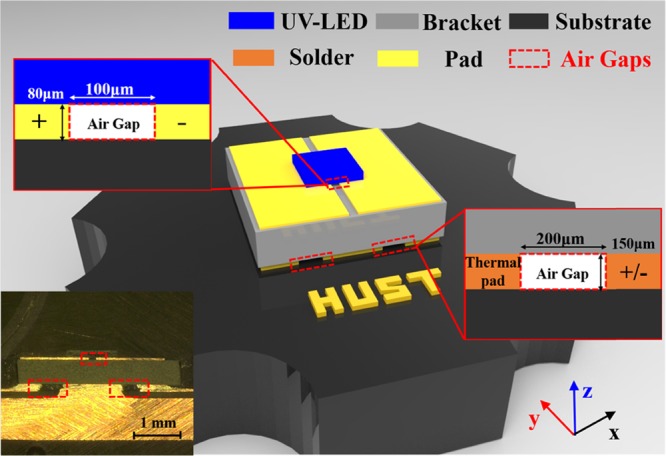
View of the surface-mounted UV-LED packaged on a metal substrate. The cross-sectional image is shown in the inset.
Figure 2.
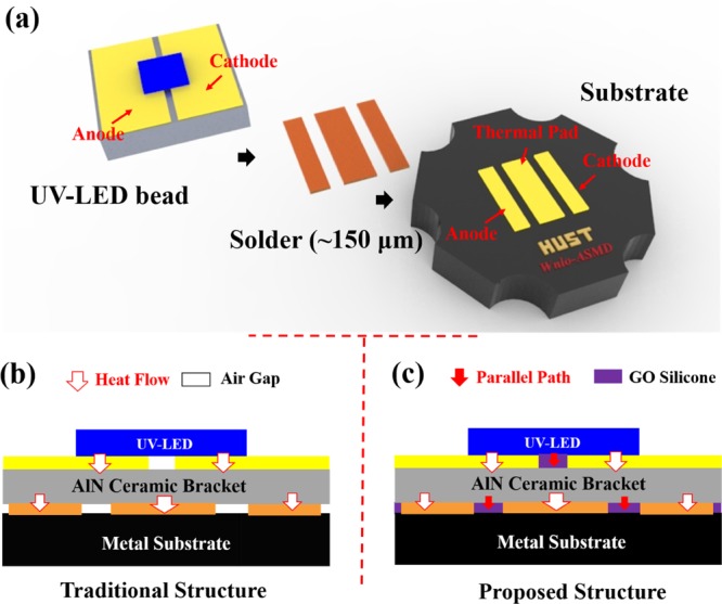
Schematics of the (a) packaging process of UV-LED bead, (b) traditional structure, and (c) proposed structure.
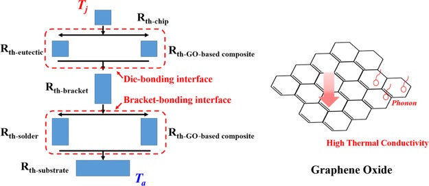
According to the heat transfer theory,28−33 the proposed structure possesses better thermal conductivity than the traditional structure, as shown in Figure 2b,c, because the air gaps in parallel with the heat flow are embedded by the GO-based composite with good thermal property and become extra thermal conductive paths.34,35 The accumulated heat in the interface can be easily transferred to the heat sink. To theoretically analyze the thermal resistance model of the proposed structure, it is simply schematized in Figure 3.
Figure 3.
Schematic of the thermal resistance model of the proposed structure.
Therefore, taking the bracket-bonding layer as an example, the following equation is established
| 1 |
where Rth-B represents the thermal resistance of the bracket-bonding interface in the proposed structure, Rth-solder is the thermal resistance of the solder, and Rth-composite is the thermal resistance of the GO-based composite. After calculating, the bracket-bonding interface thermal resistance of the proposed structure is given as
| 2 |
The bracket-bonding interface thermal resistance of the traditional structure is that of the SAC305 solder, and it is shown as
| 3 |
Therefore, the interface thermal resistance of the proposed structure is smaller than that of the traditional structure. In addition, it is the same situation in the die-bonding interface. Therefore, the heat-dissipation ability will be improved by the embedding packaging structure.
III. Results and Discussion
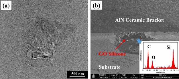
Figure 4a shows the transmission electron microscopy (TEM) image of GO obtained by the ball-milling method, which shows that the size of GO is about 1 μm. Figure 4b shows the scanning electron microscopy (SEM) image of the GO-based composite filled in the air gap, confirming that GO is randomly dispersed in the composite and wrapped efficiently in silicone, without any air gap between GO and silicone. Meanwhile, the energy-dispersive spectrometry (EDS) image (inset in Figure 4b) shows the ratio of C and O elements to confirm the existence of GO. The thermal conductivity of the 4 wt % GO-based composite was evaluated about 6.1 W/(m·K), and a relative low coefficient of thermal expansion of 130 × 10–6/K was obtained.
Figure 4.
(a) TEM image of GO and (b) SEM image of the GO-based composite embedded in the air gap. The inset shows the results of EDS.
Structure functions, including cumulative structure functions and differential structure functions, are obtained by the transient thermal resistance measurements. Structure functions provide a map of the cumulative thermal capacitances of the heat flow path with respect to the thermal resistances from the junction temperature to the ambient temperature. In the cumulative structure functions, the inflexion indicated that heat reached new interfaces in the flow path or changed surface areas in the heat flow path. The thermal resistance is large in the relatively flat region, whereas the thermal capacitance is large in the steep region. In addition, the differential structure functions are defined as the derivative of the cumulative curve. The local peaks and valleys indicate the middle of any new region, and their distance along the horizontal axis represents the partial thermal resistance between these surfaces. The wave crests indicate that the region has a high thermal conductivity, and the wave troughs indicate an area with low thermal conductivity.35−38
Sample 1 was fabricated with a low thermal conductivity aluminum substrate (dielectric coating, ∼2 W/(m·k)). The structure functions of sample 1 before and after embedding with the GO-based composite are shown in Figure 5. Accordingly, the distance between the origin and the sixth peak yields the thermal resistance from the epitaxial layer to the middle region of the thermal grease. S1 denotes sample 1 before embedding with the GO-based composite, and S*1 denotes sample 1* after embedding with the GO-based composite. Therefore, it can be observed that the junction to substrate thermal resistance (Rth-js) of the proposed structure is reduced from 19.8 to 17.1 K/W after embedding the GO-based composite under a working current of 500 mA. Moreover, the junction temperatures of the traditional and proposed structures were measured at 51.6 and 48.7 °C, respectively, to indicate that the GO-based composite can improve the thermal dissipation around structure gaps to benefit the performance of UV-LEDs.
Figure 5.
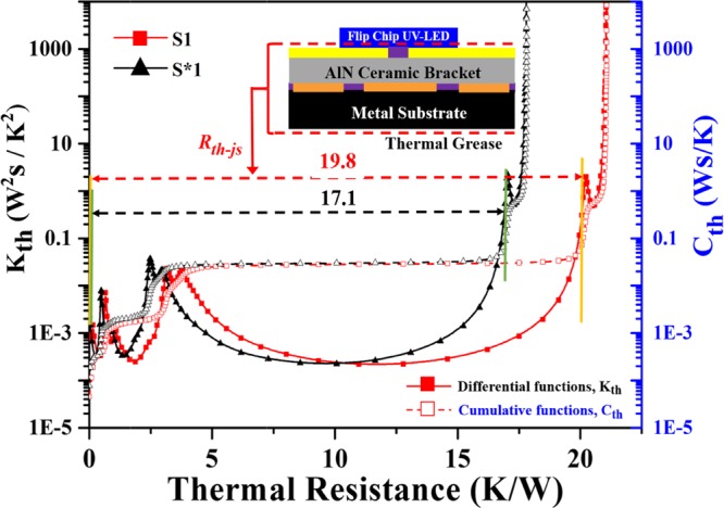
Cumulative and differential structure functions of samples 1 and 1*. S1 denotes sample 1 before embedding with the GO-based composite, and S*1 denotes sample 1* after embedding with the GO-based composite. The full line and solid legend represent the differential functions, and the imaginary line and hollow legend represent the cumulative functions.
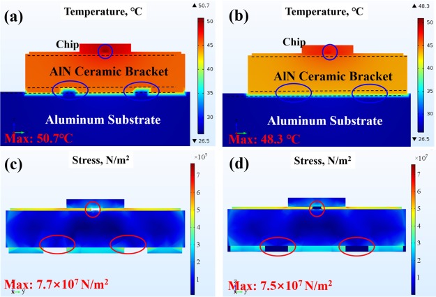
To further understand the insights of thermal behavior of the GO-based composite, the simulations for the thermal behavior of the traditional and proposed structures have been performed using FEA. The material and structural properties are the same as those in our pervious works,39,40 to help build the simulation model. The ambient temperature was fixed at 25 °C. Forced convection occurred at the bottom surface of the aluminum substrate with a stationary temperature of 25 °C, and other surfaces were cooled by convection with a heat transfer coefficient of 5 W/(m2·K). It was assumed that the filled elements formed perfect contacts between the chip and the substrate, and the air gap of the traditional structure was restricted to a sufficiently low thermal conductivity [0.026 W/(m·K) referring to air], but the thermal conductivity of the GO-based composite reached up to 6.1 W/(m·K) according to the test result. The heat flow generated from the chip is 1.260 and 1.245 W for the traditional and proposed structures, respectively, which are the experimental result. Because of the simulated cross-temperature fields shown in Figure 6a, much heat was gathered around the air gaps and the highest temperature is located at the center of the chip in the traditional structure. However, the proposed structure embedded with the GO-based composite possesses extra thermal paths to decrease the heat accumulation, leading to a decline of maximal temperature by 2.4 °C, as shown in Figure 6b. On the basis of uniform temperature distribution, a decrease of thermal stress by 2 × 10⁷ N/m2 was obtained in the proposed structure, as shown in Figure 6d. It is believed that the microholes caused by high thermal stress will be a humidity path resulting in possible structure damage;41,42 thus, the proposed structure has a promising improvement in thermal stability.
Figure 6.
Cross-sectional images of simulated temperature fields of (a) traditional structure, (b) proposed structure, and stress fields of (c) traditional structure and (d) proposed structure.
To further evaluate the effect of the heat dissipation in the interface by the proposed structure, sample 2 fabricated with a high thermal conductivity copper substrate (electrically neutral thermal path, ∼383 W/(m·k)) was investigated. Compared with that of sample 1, the total thermal resistance of sample 2 is relatively low, so the thermal resistance of interfaces could be accurately obtained. Figure 7 shows the structure functions of sample 2 before and after embedding with the GO-based composite under a working current of 1000 mA. The distance between the first and the third peaks represents the total thermal resistance of (1) the partial UV-LED chip, (2) the whole die-bonding interface, and (3) the partial AlN ceramic bracket. Analogously, the distance between the third and the fifth peaks represents the total thermal resistance of (1) the partial AlN ceramic bracket, (2) the whole bracket-bonding interface, and (3) the partial metal substrate. Accordingly, the thermal resistance of the die-bonding interface and bracket-bonding interface could be obtained by analyzing the second peak and fourth peak, respectively. The thermal resistance of the die-bonding interface of sample 2 is found to reduce by 0.16 K/W after embedding with the GO-based composite, revealing a 26.7% thermal resistance decrease in the die-bonding layer. Similarly, a 34.0% decrease of thermal resistance of the bracket-bonding interface was obtained after embedding the GO-based composite. Consequently, the proposed embedding of the GO-based composite structure can efficiently reduce the interface thermal resistance by about 30%. What is more, the total thermal resistance of sample 2 is reduced by 1.17 K/W, revealing a decrease of 21.4% after filling it with the GO-based composite.
Figure 7.
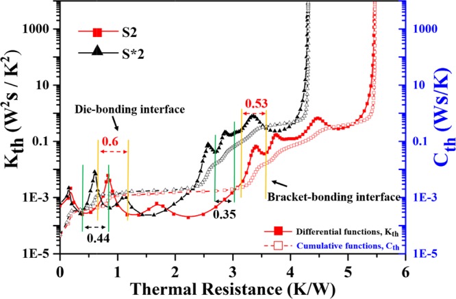
Cumulative and differential structure functions of samples 2 and 2*. S2 denotes sample 2 before embedding with the GO-based composite, and S*2 denotes sample 2* after embedding with the GO-based composite.
Figure 8 shows the junction temperature change during cooling of sample 1 and sample 2 after embedding with the GO-based composite. The working currents of sample 1 and sample 2 are 500 and 1000 mA, respectively. In the test, the bottom surfaces of the samples are maintained at a constant temperature of 25 °C by the thermostat chamber of T3Ster. Before filling sample 1 with the GO-based composite, the junction temperature of sample 1 is 26.6 °C, but after filling, the junction temperature reduces to 23.7 °C. Meanwhile, a decrease of 1.2 °C of sample 2 after filling with the GO-based composite is also obtained. Furthermore, under the working current of 1000 mA, the LOPs are 1050 and 1087 mW for sample 2 and sample 2*, respectively, with an enhancement of 3.5% in the LOP. The detailed information of LOP is displayed in Figure S6 (Supporting Information). As a result, benefited from the decrease of interface thermal resistance, the proposed embedding structure of packaging materials can reduce the junction temperature and improve the LOP, especially to effectively reduce the junction temperature of devices with high interface thermal resistance.
Figure 8.
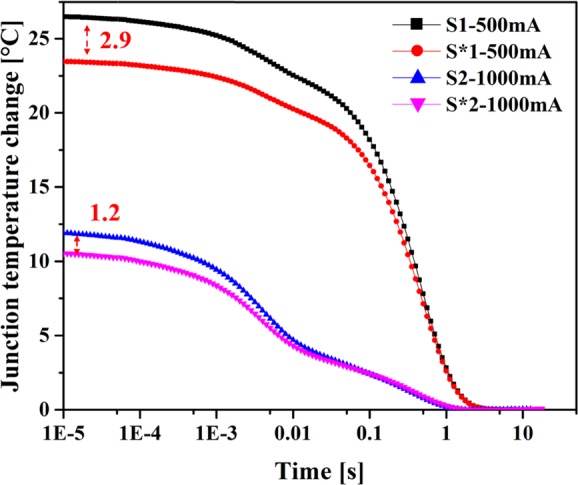
Junction temperature change of sample 1/1* and sample 2/2*.
The lifetime and thermal stability of UV-LEDs with the proposed structure were investigated by an accelerated aging test. Four samples were fabricated for this aging test: sample A and sample B were fabricated with an aluminum substrate, and sample C and sample D were fabricated with a copper substrate. Moreover, sample B and sample D were embedded with 4 wt % GO-based composite. The tests were performed at 25 °C and 90% relative humidity (RH), and the working currents of four samples were set at 1000 mA. The LOP was measured over 1000 h to confirm the long-term stability of the UV-LEDs with the proposed structure. Figure 9 shows the normalized LOP as a function of the working time. The differences of the light failure rate are obvious between the traditional structure and the proposed structure. After 1000 h, the difference in the relative LOP between the samples C and D was ca. 1.0% and it was up to ca. 2.2% between the samples A and B. This indicates that the proposed structures embedded with the GO-based composite (samples B and D) show a lower light failure rate when compared with the traditional structure (samples A and C). Therefore, embedding 4 wt % GO-based silicone composite into the packaging structure could further decrease the interface thermal resistance and improve the lifetime and thermal reliability of the UV-LED devices.
Figure 9.
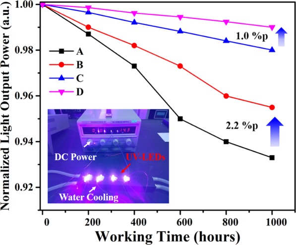
Normalized LOP of four samples as a function of the working time. Samples B and D are embedded with 4 wt % GO-based composite. The inset shows the accelerated aging process. The tests are performed at 25 °C and 90% RH, and the initial value of LOP is considered to be 1.
IV. Conclusions
In summary, GO was successfully incorporated in the silicone by the ultrasonic agitation method, which is a simple and efficient approach. The GO-based composite was applied to the surface-mounted UV-LEDs as a high thermal conductivity underfilling material. Experimental results show that the UV-LEDs embedded by the silicone composite with 4 wt % GO filler exhibit superior thermal and reliable performance by reducing the interface thermal resistance and junction temperature. The interface thermal resistance of the proposed structure can be reduced by about 34%. Meanwhile, the increase in junction temperature can also be decreased by 1.2 °C, leading to a low thermal stress. It is considered that the proposed structure has greater effect on the UV-LEDs with high interface thermal resistance. Moreover, the UV-LEDs with the proposed structure had a low light failure rate compared to the traditional structure through the accelerated aging test. Accordingly, the proposed structure embedded with the GO-based composite is believed to be promising in UV-LED applications with high-power situation.
V. Experiments
V.A. Materials
The GO powders (5–50 μm, synthetic), moldable silicone (MS-1002, Dow Corning), UV-LED chip (wavelength: 395 nm, Flip-Chip), AlN ceramic bracket (ICP Technology Co. Ltd), SAC305 solder (Senju Metal Industry Co., Ltd), and aluminum/copper substrates were used for this investigation.
V.B. Fabrication of GO-Based Composites and Packaging Process
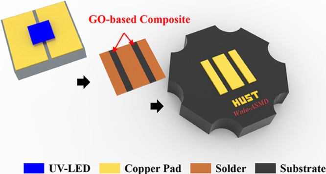
The packaging material of the GO-based composite was fabricated by ultrasonic agitation which was described in our previous work.43 As shown in Figure 10, the GO powders were first dispersed in part A of MS-1002 silicone by sonication and a planetary gravity mixer (VM300SA2, Sinomix). The air of the mixture was removed by vacuum, and the GO powders were uniformly dispersed after centrifugation. Then, part B (a curing agent, A/B weight ratio of 1:1) is added to the mixture and the GO-based silicone is ensured to be cured after heating. Finally, the GO-based composite was mixed again using the planetary gravity mixer. According to previous discussions, the interface thermal resistance decreases with the increase of the GO content, but the excess GO will make the composite conductive and viscous, and it will lead to high risk of a short circuit. Thus, the silicone composite with 4 wt % GO was fabricated and proven to exhibit good thermal conductivity, mobility, and insulativity. The UV-LED chips were bonded onto the AlN ceramic bracket by the AuSn eutectic method, and then the bracket was mounted onto the metal substrate through solder reflowing. The bonding process was described in detail within ref (44). After that, the GO-based composite was dispensed on one side of the air gap, and it would fill the whole gap under the action of vacuum and capillarity, as shown in Figure 10c. In addition, the geometric dimensioning of air gaps was measured, as seen in the cross section of Figure 10c.
Figure 10.
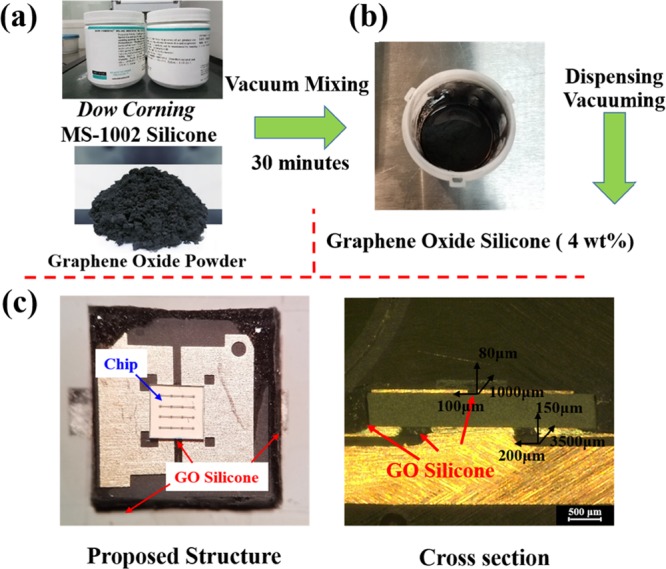
Fabrication process of the GO-based composite and proposed structure. (a) Silicone and GO powder. (b) GO-based composite via physical mixing. (c) Planform of the proposed structure on the left; cross section on the right.
V.C. Measurement
TEM, SEM, and EDS measurements were performed at the Wuhan National Laboratory for Optoelectronics (WNLO) at Huazhong University of Science and Technology. The thermal conductivity was evaluated by the thermal conductivity measurement apparatus (LW9389, Longwin, Taiwan). The thermal resistance and junction temperature of the UV-LEDs were measured using the T3Ster Master System based on the transient temperature changes during cooling, with the optical power excluded, as described in JESD51-51 standard.45 Furthermore, the thermal simulations have been performed based on the FEA.
Acknowledgments
This work is supported by the Key Project of Chinese National Development Programs (grant nos. 2016YFB0400901 and 2016YFB0400804), the Key Laboratory of Infrared Imaging Materials and Detectors, Shanghai Institute of Technical Physics, Chinese Academy of Sciences (grant no. IIMDKFJJ-15-07), the National Natural Science Foundation of China (grant nos. 61675079, 11574166, and 61377034), and the Director Fund of WNLO.
Supporting Information Available
The Supporting Information is available free of charge on the ACS Publications website at DOI: 10.1021/acsomega.7b00918.
Calculation of the volume ratio of the air gaps in the bracket-bonding layer, simulation of the proposed structure on thermal performance, measurement of LOP with traditional and proposed structures (PDF)
The authors declare no competing financial interest.
Supplementary Material
References
- Yao C.; Yang G.; Li Y.; Sun R.; Zhang Q.; Wang J.; Gao S. M. Investigation of N-face AlGaN ultraviolet light-emitting diodes with composition-varying AlGaN electron blocking layer. Opt. Quantum Electron. 2015, 48, 31. 10.1007/s11082-015-0345-5. [DOI] [Google Scholar]
- Wall F.; Ferguson I. T.; Martin P. S.; Narendran N.; DenBaars S. P.; Harbers G.; Carrano J. C. High-power LED Package Requirements. Proc. SPIE 2004, 5187, 85. 10.1117/12.512477. [DOI] [Google Scholar]
- Tadatomo K.; Okagawa H.; Ohuchi Y.; Tsunekawa T.; Imada Y.; Kato M.; Taguchi T. High output power InGaN ultraviolet light-emitting diodes fabricated on patterned substrates using metalorganic vapor phase epitaxy. Jpn. J. Appl. Phys., Part 2 2001, 40, L583–L585. 10.1143/jjap.40.l583. [DOI] [Google Scholar]
- Nishida T.; Saito H.; Kobayashi N. Efficient and high-power AlGaN-based ultraviolet light-emitting diode grown on bulk GaN. Appl. Phys. Lett. 2001, 79, 711–712. 10.1063/1.1390485. [DOI] [Google Scholar]
- Muramoto Y.; Kimura M.; Nouda S. Development and future of ultraviolet light-emitting diodes: UV-LED will replace the UV lamp. Semicond. Sci. Technol. 2014, 29, 084004. 10.1088/0268-1242/29/8/084004. [DOI] [Google Scholar]
- Arques-Orobon F. J.; Nuñez N.; Vazquez M.; Segura-Antunez C.; González-Posadas V. High-power UV-LED degradation: Continuous and cycled working condition influence. Solid-State Electron. 2015, 111, 111–117. 10.1016/j.sse.2015.05.039. [DOI] [Google Scholar]
- Kumar R. N.; Keem L. Y.; Mang N. C.; Abubakar A. Ultraviolet radiation curable epoxy resin encapsulant for light emitting diodes. J. Appl. Polym. Sci. 2006, 100, 1048–1056. 10.1002/app.23189. [DOI] [Google Scholar]
- Balandin A. A. Thermal properties of graphene and nanostructured carbon materials. Nat. Mater. 2011, 10, 569–581. 10.1038/nmat3064. [DOI] [PubMed] [Google Scholar]
- Ghosh S.; Calizo I.; Teweldebrhan D.; Pokatilov E. P.; Nika D. L.; Balandin A. A.; Bao W.; Miao F.; Lau C. N. Extremely high thermal conductivity of graphene: Prospects for thermal management applications in nanoelectronic circuits. Appl. Phys. Lett. 2008, 92, 151911. 10.1063/1.2907977. [DOI] [Google Scholar]
- Balandin A. A.; Ghosh S.; Bao W.; Calizo I.; Teweldebrhan D.; Miao F.; Lau C. N. Superior Thermal Conductivity of Single-Layer Graphene. Nano Lett. 2008, 8, 902–907. 10.1021/nl0731872. [DOI] [PubMed] [Google Scholar]
- Hummers W. S.; Offeman R. E. Preparation of Graphitic Oxide. J. Am. Chem. Soc. 1958, 80, 1339. 10.1021/ja01539a017. [DOI] [Google Scholar]
- Chen J.; Yao B.; Li C.; Shi G. An improved Hummers method for eco-friendly synthesis of graphene oxide. Carbon 2013, 64, 225–229. 10.1016/j.carbon.2013.07.055. [DOI] [Google Scholar]
- Marcano D. C.; Kosynkin D. V.; Berlin J. M.; Sinitskii A.; Sun Z.; Slesarev A.; Alemany L. B.; Lu W.; Tour J. M. Improved Synthesis of Graphene Oxide. ACS Nano 2010, 4, 4806–4814. 10.1021/nn1006368. [DOI] [PubMed] [Google Scholar]
- Yin J.; Zhu G.; Deng B. Graphene oxide (GO) enhanced polyamide (PA) thin-film nanocomposite (TFN) membrane for water purification. Desalination 2016, 379, 93–101. 10.1016/j.desal.2015.11.001. [DOI] [Google Scholar]
- Ye L.; Xiao T.; Zhao N.; Xu H.; Xiao Y.; Xu J.; Xiong Y.; Xu W. Derivitization of pristine graphene for bulk heterojunction polymeric photovoltaic devices. J. Mater. Chem. 2012, 22, 16723–16727. 10.1039/c2jm32729e. [DOI] [Google Scholar]
- Cho E.-C.; Huang J.-H.; Li C.-P.; Chang-Jian C.-W.; Lee K.-C.; Hsiao Y.-S.; Huang J.-H. Graphene-based thermoplastic composites and their application for LED thermal management. Carbon 2016, 102, 66–73. 10.1016/j.carbon.2016.01.097. [DOI] [Google Scholar]
- Ren F.; Zhu G.; Ren P.; Wang Y.; Cui X. In situ polymerization of graphene oxide and cyanate ester–epoxy with enhanced mechanical and thermal properties. Appl. Surf. Sci. 2014, 316, 549–557. 10.1016/j.apsusc.2014.07.159. [DOI] [Google Scholar]
- Zhao X.-w.; Zang C.-g.; Wen Y.-q.; Jiao Q.-j. Thermal and mechanical properties of liquid silicone rubber composites filled with functionalized graphene oxide. J. Appl. Polym. Sci. 2015, 132, 42582. 10.1002/app.42582. [DOI] [Google Scholar]
- Shahil K. M. F.; Balandin A. A. Graphene–multilayer graphene nanocomposites as highly efficient thermal interface materials. Nano Lett. 2012, 12, 861–867. 10.1021/nl203906r. [DOI] [PubMed] [Google Scholar]
- Kim C. M.; Kang Y. T. Cooling performance enhancement of LED (Light Emitting Diode) using nano-pastes for energy conversion application. Energy 2014, 76, 468–476. 10.1016/j.energy.2014.08.039. [DOI] [Google Scholar]
- Yu W.; Xie H.; Chen L.; Zhu Z.; Zhao J.; Zhang Z. Graphene based silicone thermal greases. Phys. Lett. A 2014, 378, 207–211. 10.1016/j.physleta.2013.10.017. [DOI] [Google Scholar]
- Song N.; Jiao D.; Cui S.; Hou X.; Ding P.; Shi L. Highly Anisotropic Thermal Conductivity of Layer-by-Layer Assembled Nanofibrillated Cellulose/Graphene Nanosheets Hybrid Films for Thermal Management. ACS Appl. Mater. Interfaces 2017, 9, 2924–2932. 10.1021/acsami.6b11979. [DOI] [PubMed] [Google Scholar]
- Zhang X.; Yeung K. K.; Gao Z.; Li J.; Sun H.; Xu H.; Zhang K.; Zhang M.; Chen Z.; Yuen M. M. F.; Yang S. Exceptional thermal interface properties of a three-dimensional graphene foam. Carbon 2014, 66, 201–209. 10.1016/j.carbon.2013.08.059. [DOI] [Google Scholar]
- Lee S.; Kim Y. K.; Jang J. Long-term stability improvement of light-emitting diode using highly transparent graphene oxide paste. Nanoscale 2016, 8, 17551–17559. 10.1039/c6nr05173a. [DOI] [PubMed] [Google Scholar]
- Lee S.; Hong J.-Y.; Jang J. Multifunctional Graphene Sheets Embedded in Silicone Encapsulant for Superior Performance of Light-Emitting Diodes. ACS Nano 2013, 7, 5784–5790. 10.1021/nn4024587. [DOI] [PubMed] [Google Scholar]
- Shepherd R. L.; Yerazunis W. S.; Lau K. T.; Diamond D. Low-cost surface-mount LED gas sensor. IEEE Sens. J. 2006, 6, 861–866. 10.1109/jsen.2006.877849. [DOI] [Google Scholar]
- Christensen A.; Graham S. Thermal effects in packaging high power light emitting diode arrays. Appl. Therm. Eng. 2009, 29, 364–371. 10.1016/j.applthermaleng.2008.03.019. [DOI] [Google Scholar]
- Holman J. P.Thermal Resistance and Capacity Formulation. Heat Transfer, 10th ed.; McGraw-Hill: New York, 2010; pp 176–192. [Google Scholar]
- Tao X.; Chen H.; Li S. N.; Hui S. Y. R. A New Noncontact Method for the Prediction of Both Internal Thermal Resistance and Junction Temperature of White Light-Emitting Diodes. IEEE Trans. Power Electron. 2012, 27, 2184–2192. 10.1109/tpel.2011.2169461. [DOI] [Google Scholar]
- Bagnoli P. E.; Casarosa C.; Ciampi M.; Dallago E. Thermal resistance analysis by induced transient (TRAIT) method for power electronic devices thermal characterization. I. Fundamentals and theory. IEEE Trans. Power Electron. 1998, 13, 1208–1219. 10.1109/63.728348. [DOI] [Google Scholar]
- Kim D.; Lee J.; Kim J.; Choi C.-H.; Chung W. Enhancement of heat dissipation of LED module with cupric-oxide composite coating on aluminum-alloy heat sink. Energy Convers. Manage. 2015, 106, 958–963. 10.1016/j.enconman.2015.10.049. [DOI] [Google Scholar]
- Wang J.; Zhao X.-J.; Cai Y.-X.; Zhang C.; Bao W.-W. Experimental study on the thermal management of high-power LED headlight cooling device integrated with thermoelectric cooler package. Energy Convers. Manage. 2015, 101, 532–540. 10.1016/j.enconman.2015.05.040. [DOI] [Google Scholar]
- Dong H.; Wen B.; Zhang Y.; Melnik R. Thermal Conductivity of Diamond/SiC Nano-Polycrystalline Composites and Phonon Scattering at Interfaces. ACS Omega 2017, 2, 2344–2350. 10.1021/acsomega.7b00476. [DOI] [PMC free article] [PubMed] [Google Scholar]
- Lei X.; Zheng H.; Guo X.; Zhang Z.; Wu J.; Xu C.; Liu S. Reduction of Die-Bonding Interface Thermal Resistance for High-Power LEDs Through Embedding Packaging Structure. IEEE Trans. Power Electron. 2017, 32, 5520–5526. 10.1109/tpel.2016.2609891. [DOI] [Google Scholar]
- Juntunen E.; Tapaninen O.; Sitomaniemi A.; Jamsa M.; Heikkinen V.; Karppinen M.; Karioja P. Copper-Core MCPCB With Thermal Vias for High-Power COB LED Modules. IEEE Trans. Power Electron. 2014, 29, 1410–1417. 10.1109/tpel.2013.2260769. [DOI] [Google Scholar]
- Wang C.-P.; Ying S.-P.; Su Y.-C.; Chang T.-L. Thermal Analysis of Eutectic Flip-Chip Light-Emitting Diodes Fabricated Using Copper-Coated Ceramic Substrate. IEEE Trans. Electron Devices 2015, 62, 2524–2527. 10.1109/ted.2015.2443136. [DOI] [Google Scholar]
- Lan K.; Shin M. W. Thermal Resistance Measurement of LED Package with Multichips. IEEE Trans. Compon. Packag. Technol. 2007, 30, 632–636. 10.1109/tcapt.2007.906332. [DOI] [Google Scholar]
- Kim H.-H.; Choi S.-H.; Shin S.-H.; Lee Y.-K.; Choi S.-M.; Yi S. Thermal transient characteristics of die attach in high power LED PKG. Microelectron. Reliab. 2008, 48, 445–454. 10.1016/j.microrel.2007.08.009. [DOI] [Google Scholar]
- Liang R.; Zhang J.; Wang S.; Chen Q.; Xu L.; Dai J.; Chen C. Investigation on Thermal Characterization of Eutectic Flip-Chip UV-LEDs With Different Bonding Voidage. IEEE Trans. Electron Devices 2017, 64, 1174–1179. 10.1109/ted.2017.2656240. [DOI] [Google Scholar]
- Abdelmlek K. B.; Araoud Z.; Ghnay R.; Abderrazak K.; Charrada K.; Zissis G. Effect of thermal conduction path deficiency on thermal properties of LEDs package. Appl. Therm. Eng. 2016, 102, 251–260. 10.1016/j.applthermaleng.2016.03.100. [DOI] [Google Scholar]
- Hu J.; Yang L.; Hwang W. J.; Shin M. W. Thermal and mechanical analysis of delamination in GaN-based light-emitting diode packages. J. Cryst. Growth 2006, 288, 157–161. 10.1016/j.jcrysgro.2005.12.049. [DOI] [Google Scholar]
- Hu J.; Yang L.; Shin M. W. Mechanism and thermal effect of delamination in light-emitting diode packages. Microelectron. J. 2007, 38, 157–163. 10.1016/j.mejo.2006.08.001. [DOI] [Google Scholar]
- Liang R.; Wu F.; Wang S.; Chen Q.; Dai J.; Chen C. Enhanced Optical and Thermal Performance of Eutectic Flip-Chip Ultraviolet Light-Emitting Diodes via AlN-Doped-Silicone Encapsulant. IEEE Trans. Electron Devices 2017, 64, 467–471. 10.1109/ted.2016.2637445. [DOI] [Google Scholar]
- Liang R.; Zhang J.; Wang S.; Ding T.; Dai J.; Chen C. Experimental Study on the Effects of Eutectic Voids on the Thermal Performance Within Flip-Chip Ultraviolet Light-Emitting Diodes. IEEE Trans. Compon., Packag., Manuf. Technol. 2016, 6, 1488–1492. 10.1109/tcpmt.2016.2604019. [DOI] [Google Scholar]
- Association, E. I Transient Dual Interface Test Method for the Measurement of the Thermal Resistance Junction-to-case of Semiconductor Devices with Heat Flow through a Single Path. JESD51-14, 2010. [Google Scholar]
Associated Data
This section collects any data citations, data availability statements, or supplementary materials included in this article.


