

Abstract
This article highlights the effects from composite manufacturing parameters on fiber-reinforced composite laminates modified with layers of piezoelectric thermoplastic nanofibers and a conductive electrode layer. Such modifications have been used for enabling in situ deformation measurement in high-performance aerospace and renewable energy composites. Procedures for manufacturing high-performance composites are well-known and standardized. However, this does not imply that modifications via addition of functional layers (e.g., piezoelectric nanofibers) while following the same manufacturing procedures can lead to a successful multifunctional composite structure (e.g., for enabling in situ measurement). This article challenges success of internal embedment of piezoelectric nanofibers in standard manufacturing of high-performance composites via relying on composite process specifications and parameters only. It highlights that the process parameters must be revised for manufacturing of multifunctional composites. Several methods have been used to lay up and manufacture composites such as electrospinning the thermoplastic nanofibers, processing an inter digital electrode (IDE) made by conductive epoxy–graphene resin, and prepreg autoclave manufacturing aerospace grade laminates. The purpose of fabrication of IDE was to use a resin type (HexFlow RTM6) for the conductive layer similar to that used for the composite. Thereby, material mismatch is avoided and the structural integrity is sustained via mitigation of downgrading effects on the interlaminar properties. X-ray diffraction, Fourier transform infrared spectroscopy, energy dispersive X-ray spectroscopy, and scanning electron microscopy analyses have been carried out in the material characterization phase. Pulsed thermography and ultrasonic C-scanning were used for the localization of conductive resin embedded within the composite laminates. This study also provides recommendations for enabling internally embedded piezoelectricity (and thus health-monitoring capabilities) in high-performance composite laminates.
1. Introduction
Various industries such as aerospace and renewable energy sectors intensively use polymer composite materials for their lightness and tailorable design as well as their outstanding mechanical properties. However, aviation safety regulations and reliability assurance of the structural integrity are crucial factors in driving the use of such materials in aircraft and turbine blade structures. To satisfy both, nondestructive inspection (NDI) of the structure is carried out, which is complicated, costly, and inefficient than that for metallic structures because of the multiple material structure of the composites. Moreover, existing NDI techniques are unable to detect zero-thickness interlaminar bond defects (so-called kissing and weak bonds) likely to occur in composite adhesively bonded joints1−3 or composite laminate manufacturing.4 Therefore, development of new in situ health-monitoring techniques is required. Smart composites have been developed for structural or internal deformation and damage measurement in various fields such as optoelectronics,5−11 pulsed power systems,12−14 temperature and vapor/liquid sensing,15−20 energy harvesting,21−25 and transistors and inverters.20,26−31 In such composites, addition of electric, dielectric, or other functional materials and fillers enhances the electrical properties32,33 as well as mechanical properties.34
Piezoelectric sensing has been gaining increased interest for electric measurement of deformation in structures for years but its low durability, low capability for complex parts, and limited strain-to-failure resistivity lessen its possibilities to be considered for long-term applications.35,36 Fiber optic sensing proposes a continuous and real-time health monitoring of composite structures. Its lightness, stability, nonelectromagnetic reactivity, robustness, and allowance to be used on large structures make this candidate highly promising in detections.37 Despite the advantages, fibers have relatively low mechanical strength and can irreversibly be damaged and malfunctioned. This may lead to life-span mismatch between optical fibers and high-performance composite laminates in applications.
For piezoelectric materials, the elastic strain energy of the body can be related to their dielectric energy. Thus, a proportionality can be established between the mechanical deformation of the material and an electrical signal change, for example, change in voltage.38 Categorized as polymers, they can make ideal candidates to reduce material mismatch in bonding with polymer composites (the foundation of the current paper). However, because of their particular crystallographic structure, piezoelectric materials are highly anisotropic, which means that the electrical properties vary with the orientation of the crystal.39 Thus, it is necessary to give orientation to the properties required for directional tailoring. The current research work represents a novel, rapid technology applicable to large structures that use electrospinning technique to produce ultrathin unidirectional polyvinylidene fluoride (PVDF) nanofibers and embed such materials onto the laminates in situ. Introduction of thermoplastic veils and films has already proven durable and thermally stable candidates for the purpose of interlaminar toughening in composite laminate manufacturing (e.g., see ref (4)). However, their thickness is at the level of ply thickness, for example, 200 μm, and therefore, addition to the overall thickness of the structure is considerable. Also, such introduction of veils is not fully automated yet and can also have significant increasing effect on the overall weight of a laminated structure (if added over each ply). The proposed technology in the current article will have almost zero weight and thickness penalty at its scale-up.
PVDF is a fluoropolymer thermoplastic resulting from the polymerization of vinylidene difluoride.39 PVDF is chemically stable that prevents from chemical reaction when this material is introduced into a system and shows good resistance to oxidation and UV light.40 This polymer is naturally piezoelectric and belongs to the electroactive polymer family.39 PVDF has a semicrystalline polymorphic structure with five phases of α, β, γ, δ, and ε. The first three phases are the most commonly used in in situ measurement applications.41 The PVDF polymer chain is composed of two types of groups: CF2 fluorine group (electrically negative) and CH2 hydrogen group (electrically positive). Depending on the localization of these groups along the chain, an electrical dipole moment is generated (approximately 5–8 × 10–30 C.m). Thus, its use is appropriate for sensor and actuator development.42
The electrospinning process is commonly used to produce PVDF nanofibers. The purpose of this study was to rapidly produce highly oriented PVDF nanofibers and lay up over high-performance thermoset composite laminates for enabling internal in situ measurement in composite aircraft structures. During the curing process of the laminates, the PVDF material undergoes high temperature (>Tm) and constant pressure for a certain duration depending on the composite process specifications. As a result, PVDF may undergo a new phase transformation. The variation of the piezoelectric response of the material after PVDF being subjected to temperature treatments has already been reported.43 Therefore, the loss of performance of the material under temperature treatment has quantitatively been evaluated.
According to a study on stretched PVDF, the transformation of α phase into β phase seems to be more affected by the stretching ratio than the stretching temperature.44 Because of the use of aerospace prepregnated thermoset composite pre-pregs for manufacturing composite laminates, heat energy at relatively high temperature (>120 °C) is required for the curing to be effective, for example, approx. 180 °C for carbon fiber pre-pregs. Reticulation occurs between polymer chains, which leads to strongest bonds within the structure and solidification of the material. The melting temperature of the PVDF material is 171–175 °C, which means that during curing, the PVDF fibers will be partially molten. This means that the piezoelectric capability of PVDF fibers may still be valid after high-temperature exposure. The study in this article aims to present what piezoelectric capabilities can be left at the postprocess stage, where the material is solidified for high-performance structural applications. The paper is divided to a number of sections to address such aim: section 2 presents data for the materials used in this study and the manufacturing steps to develop an integrated composite laminate-PVDF-inter digital electrode (IDE). The section also provides theoretical background for definition of an IDE layout and discusses limitations with the manufacturing steps taken. Characterization and microscopy techniques used on the postprocessed manufactured laminates are also explained. Section 3 presents the results obtained from the techniques described in the latter section and discusses the possibility of the presence of piezoelectric phases pre- and post-manufacturing. Section 4 presents data from pulsed thermography and ultrasound NDI techniques and in connection with the results presented in section 5 discusses the effect of manufacturing steps on the mechanical performance of such an integrated multimaterial laminate.
2. Materials and Manufacturing
The current research addresses aerospace and renewable energy applications, which means that the relevant standards must be followed for the manufacturing choices: type of fibers and resin, stacking sequence, curing cycles, and so forth. To do so, the materials (as described below) were processed according to composite process specifications provided in product datasheet.45
2.1. Materials
The following structural grade materials were selected. Table 1 presents the materials and the reason they were chosen. The materials were then processed according to the specifications provided by the suppliers, for example, Hexcel. The relevant standards used for such processes45 were followed to ensure reliability of processes.
Table 1. Materials Used in the Study: Description and Reason of Their Selectiona.
| material | commercial name | company | description and relevant properties | reason of their selection |
|---|---|---|---|---|
| pre-preg unidirectional carbon fiber-reinforced thermoset composite | HexPly M21/35%/268/T700 GC | Hexcel | high-performance aerospace grade, carbon fiber–epoxy pre-preg, dedicated to structural parts. Thickness of one ply: ∼0.25 mm; curing temperature: 180 °C | high performance laminate, easy to deform, shape and manufacture |
| PVDF fibers | PVDF FibroTend | Munro Technology Limited | piezoelectric thermoplastic (PVDF) nanofibers produced by electrospinning and are highly oriented. Fiber diameter: ∼1.5 μm | desirable piezoelectric properties of the nanofibers |
| epoxy resin | HexFlow RTM6 | Hexcel | premixed epoxy system. Curing temperature: 180 °C | similar resin to the one composing the pre-preg. A great bonding is aimed between the laminate and additional elements |
| graphene powder | CamGraph G1 A | FGV Cambridge Nanosystems | ultrahigh-quality graphene powder. Density: ∼26.8 g/L | high quality and conductivity for a very low density. Appropriate for mixing into an epoxy resin for IDE fabrication |
All of these materials were chosen for their high quality, innovative, and reliable aspects for the manufacturing steps taken during the project.
The composite laminates were manufactured using unidirectional carbon fiber-reinforced thermoset polymer pre-pregs made of high-toughness resin (M21). Each cured ply had the thickness of approximately 0.125 mm (cured using an autoclave according to the specifications of the supplier). The plies were stacked to make quasi-isotropic configuration, and the PVDF and conductive layer were added just below the upper ply. The laminate was then vacuum-bagged and heated at 180 °C for a duration of 2 h under 7 bar constant pressure.
2.2. Integrated Composite Laminate Definition
The stacking sequence of the composite laminate was chosen to be symmetric and quasi-isotropic, [−45/+45/90/0]s, which enables producing composite samples with approximately homogenized isotropic properties. Figure 1 schematically shows the main composition of the laminate. The PVDF layer was set to be embedded just one layer beneath the upper ply of the laminate. That would introduce sufficient justification of internal embedment of an in situ measurement capability rather than a severe consideration, for example, embedment in the middle layer.
Figure 1.
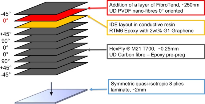
Quasi-isotropic stacking sequence of integrated composite laminates.
2.3. Polymer-Based IDE Layout Definition
The IDE layer plays a central role in the laminate for a health-monitoring purpose. The two types of unimorph electrodes (d33 and d31) were initially considered. However, because of the porous morphology of the piezoelectric, a reliable electrode with a d33 configuration appeared to be too risky. FibroTend layer is ultrathin (∼250 nm to 1 μm) and composed of numerous fibers, which would easily let a conductive resin flow through it during the curing cycle, leading to short circuits. Therefore, the simple d33 configuration was abandoned for a d31 configuration. The main difficulty was to make sure that the IDE would be an integrated part of the laminate to serve structural integrity (i.e., not acting as an external object/defect) by an effective bonding between the IDE and the pre-pregs. This aspect is novel and such introduction has rarely been exercised. The IDE layout was developed using graphene mixing in a resin (RTM6) similar to that of the composite laminate (M21) over the PVDF layer (Figure 1). Therefore, curing of the resin from both pre-preg and the IDE was done simultaneously to produce strong bonding as the layout was then an integrated part of the structure. However, a drawback in such an integration technique was that the layout resin was allowed to flow during autoclave processing and as such, there was no control on its change of geometry. To avoid possible short circuits during such a flow, the authors took a theoretical step for design of the IDE layout with the widest possible spacing according to the recommendations provided in the following section.
2.3.1. Design of the IDE Layout for Composite Integration
According to studies done on piezoelectric ceramic materials, the IDE layout strongly influences the performance of a measurement system.46 Referring to the definition of the IDE layout in the previous section, it has been shown that the following relationships should be considered for optimizing the IDE layout performances46
| 1 |
where
| 2 |
Another study with a metal IDE on a piezoelectric polymer [poly(3-hexylthiophene-2,5-diyl)] confirms that w must be maximized and s must be minimized.47 The piezoelectric FibroTend layer provided in this study has a minimum thickness of ∼250 nm, which allowed for calculating the thickness of the electrode fingers
| 3 |
Thus: we = 0.8 . 250 = 200 nm.
Moreover, the samples were initially designed following the ASTM 7264 standard for the four-point bending mechanical testing after manufacturing. This led to a sample size of 13 mm × 90 mm × 2 mm with a potential electrode width of w = 10 mm. Thus, with a least restrictive w/s ratio of 6, the finger spacing was s = 1.7 mm.
According to the choice of the resin dispersion method, the nanoscale dispersion appeared difficult to achieve. Therefore, the electrode layout was scaled up to a millimeter scale with larger electrode fingers (we) and larger finger spacing (s). Also, s should be minimized compared to w which should be maximized. The electrode is placed/printed at the center of the length of the sample, and the length of the electrode is limited to fit with the span of the upper clamping fixtures used for applying the mechanical load. This condition is required to ensure that the electrode is not damaged because of the introduction of localized stress from the fixtures in contact with the sample. Therefore, the dimensions of the sample were reviewed for the specific purpose of integrating with the composite laminate and recommended as below (shown in Figure 2).
Figure 2.
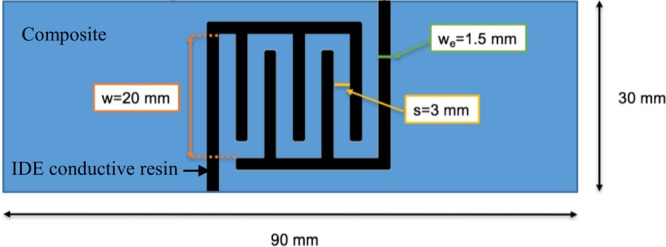
Schematic of the scaled-up IDE electrode layout for composite integration.
The width of the sample was increased to 30 mm with the electrode width w of 20 mm. The electrode finger width we was set at 1.5 mm and the spacing between the fingers to 3 mm. This scale-up led to the following ratios: we/hp = 12 and w/s = 6.67.
2.3.2. Conductive Resin
Graphene was supplied in a powder form by Cambridge Nanosystems (Table 1) for mixing the powder into the epoxy resin. Therefore, the laboratory risk assessment imposed a use limited to 1 g of powder. It has been shown that the increasing weight percentage of graphene in the resin has an increasing effect on the electrical conductivity of the resin. Several studies with different polymer and graphene types show a similar specific trend: conductivity increases significantly with graphene content up to reaching a threshold circa 2 wt % graphene filler.48
Accordingly, the conductivity of the resin examined in this study was increased via high shear mixing of graphene nanopowders composing of
•40 g of HexFlow RTM6 epoxy resin and
•0.8 g of CamGraph G1 A graphene powder,
which result in an approximately 2 wt % concentration of graphene in the epoxy resin. Trials on high shear mixing and ultrasonic exfoliation were carried out to avoid/mitigate the presence of high agglomeration. There was no control on reagglomeration during the composite laminate manufacturing process; however, the authors emphasize that the current research has mainly been focused on the effect of composite processing on the presence of piezoelectric phases rather than reagglomeration.
2.4. Laminate Manufacturing
The following steps have been followed to manufacture the modified integrated composite laminate:
-
(1)
Cutting pre-pregs at the neat size of the final sample (30 mm × 90 mm), with the relevant orientation of 0°, 45°, or 90°.
-
(2)
Stacking of the pre-preg pieces in the quasi-isotropic order (Figure 1).
-
(3)
Deposition of the conductive resin using jet printing.
-
(4)
Finishing the laminate with the last eighth ply on which the piezoelectric FibroTend had already been deposited via electrospinning, as shown in Figure 3. This ply must be integrated with the layer of piezoelectric nanofibers directly in contact with the electrode to have a close electrical circuit.
-
(5)
All samples were placed and layed up with the FibroTend layer on top for autoclave processing. In addition of the required release films for vacuum-bagging, a metal plate was placed on top of the samples to ensure uniform pressurization during the curing process. Standard curing cycle as specified in the Hexply specifications45 (shown in Figure 5) was conducted. Hexcel provides two standard curing cycles for laminates composed of Hexply M21 T700 CF–epoxy pre-preg having thicknesses of <15 mm: one with a heat-up rate at 1 °C/min and a second at 3 °C/min. The curing cycle with a heat-up rate of 1 °C/min was selected for this study so as to limit the flow of the conductive electrode resin. Viscosity and the resin flow decrease with the duration, whereas temperature constantly increases. The trend in viscosity changes after 100 min according to the Hexply specifications, that is, it embarks on a sharp increase with time. A lower heat-up rate enables to moderate the viscosity drop until the resin reticulates for times <100 min and thus significantly reduces the chance of high resin flow and thus short circuits in the IDE layout.
Figure 3.
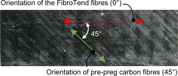
Eighth ply, Hexply M21 carbon composite (45°) with PVDF FibroTend nanofibers on top (0°).
Figure 5.
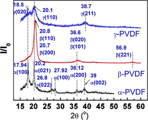
XRD patterns of the three α, β, and γ phases, with both peak angles and (hkl) planes.52
To assess the influence of the laminate modification (i.e., addition of a FibroTend layer and an electrode), eight additional samples were also manufactured with no FibroTend-IDE layer. These samples are referred to as reference samples in this paper.
2.5. Characterization of PVDF Materials
Scanning electron microscopy (SEM), energy dispersive X-ray spectroscopy (EDXS), X-ray diffraction (XRD), and Fourier transform infrared (FTIR) spectroscopy characterization techniques were used for analysis of the morphology and crystal phases of five categories of samples, which are labeled and tabulated in Table 2.
Table 2. Five Categories of PVDFs Used for Morphological Analysis and Phase Characterization.
| # | name | description |
|---|---|---|
| 1 | FibroTend 1 | electrospun oriented PVDF fibers stretched to 100 mm (+25%) and twisted into a bundle |
| 2 | FibroTend 2 | electrospun oriented PVDF fibers stretched to 320 mm (+300%) and twisted into a bundle |
| 3 | FibroTend 3 | electrospun oriented PVDF fibers stretched to 320 mm (+300%) and deposited on an aluminum foil (highly oriented) 1.2 gsm |
| 4 | PVDF powder | neat PVDF powder Solvay Solef 6020/1001 |
| 5 | Finetex | unaligned mat of electrospun PVDF fibers, 8.5 gsm |
2.6. Postmanufacturing Analysis
The integrated laminates were also analyzed after manufacturing using the characterization techniques described above. The objectives were to understand the IDE pattern localization, the FibroTend piezoelectric characteristics after curing, the electrical capability of the cured graphene–epoxy resin, and the effects of such multimaterial integration taken in this study on the mechanical properties. Pulsed thermography, ultrasonic C-scanning, XRD, FTIR spectroscopy, and electrical resistance testing were used for post integration stage of the study.
3. Results and Discussion
3.1. Raw Material Characterization
This section presents data from the characterization and microscopy techniques described in section 2. Four techniques were used for the morphology analysis and crystal-phase characterization.
FEI/Philips XL30 SEM was used to visually analyze the sample quality, homogeneity, and morphology. Estimation of the contamination level and composition was also carried out using EDXS in the scanning electron microscope. Samples for such measurements were vacuumed at 25 °C and gold-coated on the surface by an approx. 5–10 nm thickness layer. X-ray measurements were carried out using a Siemens D5005 X-ray diffractometer to determine the piezoelectric phases. The samples for such a measurement were different in size and shape according to Table 2; however, all samples were cleaned off under vacuum for 30 min. FTIR spectroscopy was also carried out using Jacson FTIR 6200ATR ZnSe, and the samples were treated under vacuum for 5 min each.
3.1.1. Scanning Electron Microscopy
Powder sample exhibited a homogeneous sphere size with average diameter of approximately 100 μm, as shown in Figure 4a. The Finetex sample showed an unaligned mat of fibers (Figure 4b), with average fiber diameter of ∼150 nm. Some beading and significant variation in the thickness of the fibers can also be observed, as well as no overall trend in orientation as shown in Figure 4b. The FibroTend 1 bundled fiber sample (stretched by 100 mm, 25%) showed different fiber sizes (Figure 4c), with many in excess of 2 μm in diameter (average diameter ≈ 2.3 μm). The FibroTend 2 sample (stretched by 320 mm, 300%) clearly showed significantly more damaged and broken fibers (Figure 4d), resulting from those that did not survive the stretching electrospinning process. At present, there is no mechanism for removing these fibers, but as can be seen in Figure 4d, they pose a relatively minor surface contamination compared to the bulk of the sample. The average fiber diameter was expectedly lower (<1.5 μm) for the stretched sample FibroTend 2 than for FibroTend 1.
Figure 4.
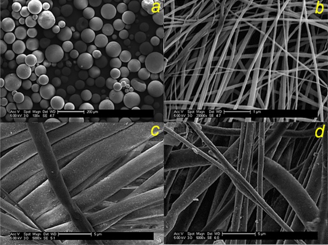
SEM images of (a) PVDF raw powder, (b) Finetex, (c) FibroTend 1, and (d) FibroTend 2.
The FibroTend samples were significantly thicker than the fibers observed from the Finetex sample. Also, because of the bundled nature of the samples supplied by Munro Technology Limited, it was not possible to observe the overall trends in fiber alignment.
3.1.2. Energy Dispersive X-ray Spectroscopy
EDXS spectra were collected from the PVDF powder, Finetex, and FibroTend 1 and 2, and analysis was performed multiple times per sample to generate a robust statistical distribution. FibroTend 3 was processed precisely identical to FibroTend 2, however, on an aluminum substrate and thus was not characterized. Results from the powder indicated a carbon:fluorine ratio of between 4:1 and 2:1, indicating significant sample contamination, as the expected result was a 1:1 ratio of carbon to fluorine (PVDF unit cell is −C2F2H2−). Finetex gave a C/F ratio of 56.5:43.5 based on a relatively large area scan, much closer to the expected values. However, looking at relatively small areas gave much lower values for fluorine content, as low as 15%. That might be explained by a higher detection of the carbon tape on which the Finetex is stuck depending on the sample regions studied (sign of inhomogeneity of the mat porosity). Spectroscopy of the FibroTend fibers (1 and 2) resulted in a wide range of results across the sample, ranging from 10 to 50%, indicating a wide margin of error, perhaps resulting from thin material samples, or contamination resulting from handling of the fibers.
The disparity between small-scale and large-area measurements indicated that in certain areas of the fiber, carbon-based contamination has occurred to increase the apparent percentage of carbon observed. This contamination can come from the manufacturing process, manipulation, and detection of the carbon tape on which the sample is stuck for being analyzed. As no sample exceeded a fluorine ratio of 50%, it can be assumed that this is an accurate assumption. No peak that could be attributed to any other atomic element than carbon, fluorine, or gold (coating) was identified. In particular, no nitrogen was observed in any of the spectra of the prepared fibers, indicating that a negligible amount of solvent was present.
3.1.3. X-ray Diffraction
For determination of the PVDF phase present in the material, an XRD analysis was carried out.49−52Figure 5 depicts a typical XRD patterns of the three α, β, and γ phases in a PVDF material, with both peak angles and (hkl) planes.52
Before analyzing the spectrums in details, it is necessary to highlight a technical limitation of performing XRD on PVDF FibroTend nanofibers provided. The amount of material required to produce a valid data is hardly compatible with the nanoscale of the fibers. Therefore, the following procedure was employed:
Powder: sufficient amount of the material and reliable method. Reliable data were obtained.
Finetex: after several attempts, a full A4 sheet of PVDF has been folded and stuck on a glass holder. The result is acceptable. However, a higher uncertainty of the measurement should be taken into account because of the less dense sample (it is difficult to compress the folded sheet).
FibroTend 1, 2, and 3: a full A4 amount of PVDF nanofiber has been doubled and folded on a glass holder. The quality of the measurement is similar to that of the Finetex.
Fibers could have been grinded into powder; however, the risk of the phase change was likely. Therefore, this option was not considered. For the three types of PVDF samples, the spectrum obtained presented a similar structure: significant (high intensity) peaks between 17° and 23°, limited (medium intensity) peaks between 24° and 41°, and a flat and nonsignificant (low intensity) shape elsewhere, as displayed in Figure 6. The measurement was carried out from 10° to 60°, but only a magnified view between 14° and 42° is presented for readability of the report. Note that FibroTend 1 and 2 spectrums are not displayed in the figure as no significant difference can be identified with the FibroTend 3 spectrum. It implies that the level of electrospinning stretching between +25 and +300% leads to the same crystal composition.
Figure 6.
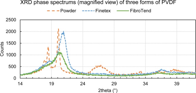
XRD phase spectrums of three forms of analyzed PVDF, ranging from 14° to 42°.
It can be noticed that some peaks are particularly distinct (high and sharp), whereas others are broader. When a peak is broad, it is difficult to associate a single value of angle, as in such cases, the uncertainty of the spectrum reading and the inaccuracy of the conclusion increases. From these three graphs, Table 3 can be extracted. It gathers 2θ angles associated with the peaks observed from each spectrum. They are sorted by the PVDF phase they represent.
Table 3. Summary of XRD Phase Results for PVDF Powder, Finetex, and FibroTend.
| sample | angle (2θ, deg) | crystal phase associated |
|---|---|---|
| powder | 17.9, (20.1), 26.5, 26.8, 36, 39.1 | Α |
| Β | ||
| 18.5, 20.1, 26.8, 38.6 | Γ | |
| Finetex | Α | |
| 20.8, 36.5 | Β | |
| Γ | ||
| FibroTend | (20.1) | Α |
| 20.3 | Β | |
| 20.2 | γ |
Because the reliable quality of the powder spectrum, it can be concluded that it is composed of α and/or β phases. Some characteristic peaks from those two phases (at 20.1° and 26.8°) are very close to each other, which leads to an ambiguous reading of the spectrum. Regarding Finetex and FibroTend, spectrums are poor; only few peaks on each spectrum can be analyzed. In addition, these peaks are really broad, which does not allow us to conclude with a high certainty that both samples made of the stretched fibers are composed of the β crystal phase. In the Finetex spectrum, only β phase characteristic peaks (20.8° and 36.5°) seem to fit with the peaks obtained. Thus, the PVDF sheet must be mainly composed of β crystal phase. For FibroTend, the result is less apparent. The single broad peak obtained can be associated with the three crystal phases (20.1°, 20.3°, and 20.2°). No certain conclusion can be made from this spectrum.
The three XRD spectrums are not sufficiently reliable to status on the crystal phase composition of PVDF powder, Finetex, and FibroTend. Therefore, further characterization was carried out. Using a second analytical technique such as Raman spectroscopy or FTIR spectroscopy technique would allow us to remove the doubt on powder (α and/or γ) and FibroTend (β and/or α) phase composition and confirm the β phase composition of Finetex. Also, unlikely to XRD phase analysis, an interest of the FTIR analysis is to be quantitative. It enables us to understand better the proportion of each phase within the material.
3.1.4. FTIR Spectroscopy
FTIR wavenumbers (cm–1) analyzed in some previous studies for PVDF material are studied.44,50,51,53−55 The absorbance band 840 cm–1 can be associated to both β and γ phases because of their really close vibrational frequencies. However, a shoulder of the 840 cm–1 peak at 833 cm–1 can be observed for the γ phase only.50 To distinguish more clearly those two β and γ phases, further comparisons should be considered such as peaks at 1275 cm–1 (for β) and 1234 cm–1 (for γ), which are specific to each phase. In Figure 7, the most interesting characteristic peaks for distinguishing α, β, and γ crystal phases are displayed.
Figure 7.
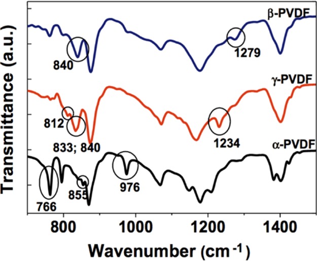
Comparison of FTIR spectrums for α, β, and γ PVDF crystal phases.50
The five experimental spectrums obtained present similar overall spectrums. Figure 8 displays the FTIR attenuated total reflectance ZnSe spectrums of the five forms of PVDF analyzed. Most of the peaks are between 550 and 1450 cm–1. Below 550 cm–1, the quality of the measurement is too dependent on the device, which makes it unreliable. Above 1450 cm–1, all spectrums are flat with limited peaks.
Figure 8.
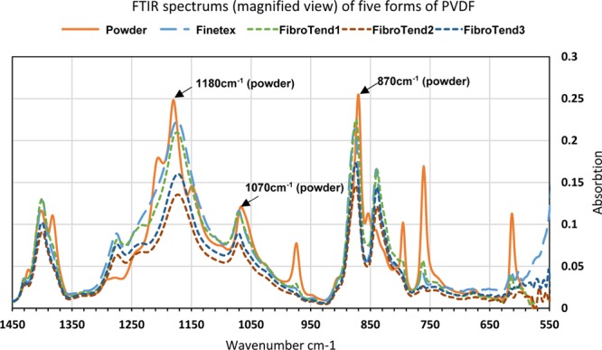
FTIR spectrums of the five forms of PVDF analyzed, selected range from 550 to 1450 cm–1.
It can be observed that the trend in the appearance of the peaks is the same for the five spectrums. However, the powder spectrum seems slightly different to the other four, with some peak shifts (around 870, 1070, or 1180 cm–1) and higher additional peaks at approx. 612, 760, 795, 1207, or 1384 cm–1. The powder is the raw material and has not been stretched unlike the other samples. To understand better the impact of electrospinning on the PVDF phase, it is required to compare the powder composition (initial raw material) with the highly stretched, processed fibers (e.g., FibroTend 3). Previously, the XRD results in Figure 6 and Table 3 showed that the level of electrospinning stretching between +25% (FibroTend 1) and +300% (FibroTend 2, 3) leads to the same crystal composition. This has also been stressed herein by the FTIR data. Table 4 tabulates each spectrum wavenumbers in association with the peaks observed.
Table 4. Summary of FTIR Results for PVDF Powder, Finetex, and FibroTend 3.
| sample | wavenumber (cm–1) | PVDF phase associated |
|---|---|---|
| PVDF powder | 613, 760, 855, 975, 1207, 1383 | Α |
| (846), (1275) | Β | |
| (846) | Γ | |
| Finetex | (976), (618) | Α |
| 840, 1175, 1275 | Β | |
| 840, 1175 | Γ | |
| FibroTend 3 | Α | |
| (747), 838, 1168, 1273, | Β | |
| (815), 840, 1175, (1236) | Γ |
To conclude, the PVDF powder is mainly composed of α phase, with some potential traces of β and γ phases. This is in agreement with the XRD results, so the powder crystal composition can be considered as confirmed and reliable for further studies. Finetex spectrum displays two peaks (840 and 1175 cm–1), which are common to both β and γ phases. However, there is a distinct peak at 1275 cm–1 and no peak at 1234 cm–1, which are corresponding to the singular peaks distinguishing the β phase from the γ phase. This leads to the conclusion in agreement with the XRD results that the Finetex sample is mainly composed of the β crystal phase. Regarding the FibroTend, many peaks corresponds to β or γ phases. However, β peaks are more dominant (higher than the other representative peaks and more distinct). Therefore, it can be considered that the FibroTend fibers are mainly composed of β phase, though some γ phase is remaining. These results from XRD and FTIR spectroscopy are logical with the manufacturing process that the PVDF powder, Finetex, and FibroTend undergo and are schematically shown in Figure 9.
Figure 9.
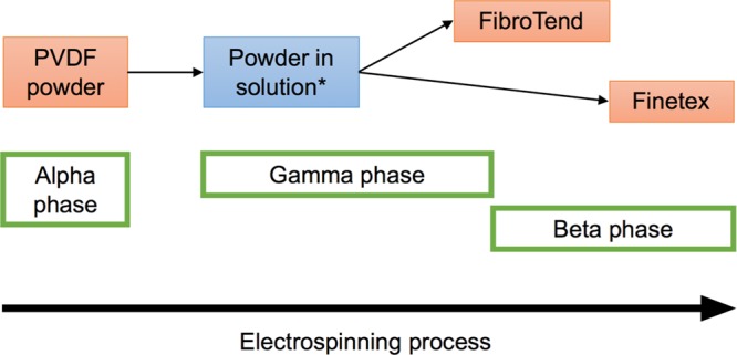
PVDF crystal phases related to electrospinning process; *in the case of FibroTend electrospinning PVDF powder was diluted in DMF.
FibroTend was stretched up to an average fiber diameter of ∼1.5 μm, whereas Finetex was stretched up to ∼150 nm. The α phase is the easiest to produce and the most chemically stable and inert phase, which is a strong interest for commercialization purpose of raw PVDF powder. The β phase can be achieved after mechanical stretching, such as electrospinning. This process stretches and aligns polymer fibers and leads to a reorganization of the polymer chain. Both Finetex and FibroTend are mainly composed of this process. The γ phase remains from the dissolution of the raw PVDF powder into dimethylformamide (DMF), preliminary of the electrospinning. The efficiency of the process is not 100%, which justifies why not all of the material is made of β phase and explains the lower traces of γ phase remaining in Finetex.
3.2. Postprocessed Material Characterization
Once composite pre-pregs, PVDF, and the conductive IDE layer were layed up, the laminate was cured to integrate the layers. A new set of XRD and FTIR analysis was then carried out to understand the impact of the curing parameters (temperature, duration, and pressure) on the PVDF crystal phase and to identify any piezoelectric remnant phases as curing-linked modification of the phases may lead to reduction of piezoelectricity capability.
3.2.1. X-ray Diffraction
XRD phase analysis on the integrated composite laminates was carried out. However, for this study, the FibroTend layer embedded between composite plies (having had ∼200 μm thickness) was too thin (∼250 nm) and the amount of material was not sufficient for determining the crystal phase. As seen in Figure 10, no peak previously observed with the raw PVDF material (Figure 6) was detected. Figure 10 shows that the integrated and the reference (with no PVDF-IDE layers) samples have similar spectrums. This confirms that only the main laminate structure (carbon fiber and epoxy resin) contributes to the detections. A slight increase (∼3%) of the main peak (around 25.5°) was observed for the integrated sample. This is due to the detection of graphene present in the conductive resin forming the conductive layer.56,57
Figure 10.
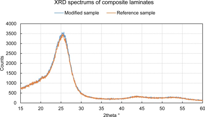
XRD spectrums of both modified and reference composite laminates.
3.2.2. FTIR Spectroscopy
FTIR spectroscopy was performed on the integrated and reference samples. Similar to XRD results, no characteristic peak previously seen with the PVDF raw material (Figure 8) can be observed on the integrated sample spectrum, displayed in Figure 11. Also, no significant difference can be observed between the integrated and reference sample spectrums, except a lower intensity of the integrated sample spectrum. This attributes to the presence of additional conductive resin absorbing energy provided for the analysis, which lessen the output energy detected.
Figure 11.
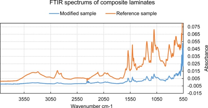
FTIR spectrums of both modified and reference composite laminates.
To conclude, postmanufacturing material characterization with XRD and FTIR techniques did not allow us to identify the PVDF FibroTend crystal phase. A new set of experimentations will be highly valuable to understand better the impact of the curing features on the PVDF piezoelectric crystal phase, and also, samples with a thicker FibroTend layer may provide a clearer spectrum.
3.2.3. Electrical Resistance Characterization
Even though the conductive resin from the IDE layout has flown during the processing, an electrical resistance was able to be measured, using a coarse range of 1–100 MΩ. The resistivity was approximately 2.5–35 MΩ comparable to that of the layer cured for initial trials outside the laminate. This clearly shows that there is either no or slight short circuit because of resin flow or contact with carbon fibers during laminate embedment and curing. The IDE design recommendations in section 2.3 were then able to efficiently enable internal conductive layer embedment. As aforementioned, such an embedment technology is highly advantageous and superior to current state-of-the-arts as the conductive nanoparticles have been distributed inside a thermoset polymer resin which is identical to the polymer matrix of the composite. Such a similarity should provide enhanced structural integrity via avoiding bond degradation due to material mismatch. NDI and mechanical testing have followed the manufacturing step to investigate the enhancements. The following sections presents their results.
4. NDI Data
The NDI data are presented in this section only for the composite laminates post cure, the two types of integrated laminate (internally embedded with PVDF-conductive layers) and the reference laminate (only carbon composite pre-pregs). NDI was carried out on the samples prior to mechanical testing.
4.1. Pulsed Thermography
Two types of comparisons were achieved with the two samples:
-
1.
On the integrated sample, comparison of a region with the central conductive resin and a region without it (at samples runways/corners) and
-
2.
comparison between samples with and without FibroTend-conductive layers.
The pulsed thermography examinations showed that the thermal diffusivity behavior is different in regions containing or not containing the conductive resin, within a sample containing the FibroTend layer (Figure 12). This is due to a difference in thermal conductivity of the two samples linked to the presence of graphene nanomaterials, which in this case is enhanced by the conductive resin (Figure 13). The difference can be distinguished clearly in figures showing the 1st and 2nd derivatives of the thermal decay behavior (Figures 13c,d and 14), respectively, representing the rate and acceleration of the decay with respect to time. This qualitative analysis is to highlight that flash thermography may be interesting to assess the quality of the manufacturing (e.g., curing state) based on the NDI response of the rein-based electrode layout.
Figure 12.
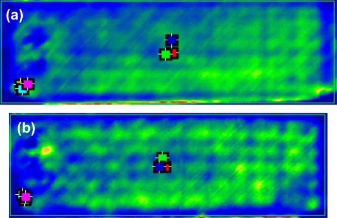
Thermal decay contours at 2 seconds post flashing of the samples: (a) reference sample and (b) integrated laminate sample (with FibroTend-conductive layer) (dimensions of the sample: 30 × 90 mm).
Figure 13.

Evolution of thermal decay with time at center and corner of the samples for (a) reference sample, (b) integrated laminate sample (with FibroTend-conductive layer), (c) 1st derivative of thermal decay for both samples, and (d) 2nd derivative of thermal decay for both samples.
Figure 14.
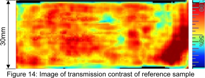
Image of transmission contrast of the reference sample.
4.2. Ultrasonic C-Scanning
Figures 14 and 15 show ultrasound C-scanning images of the reference and integrated samples, respectively. Results for all samples per each type were consistent. Therefore, one representative sample per each type only is shown below.
Figure 15.
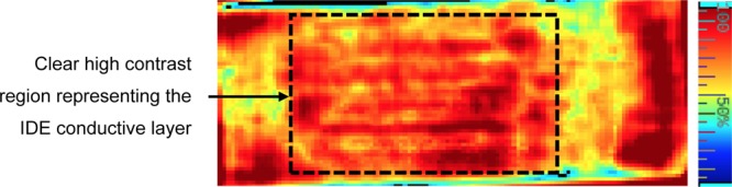
Image of transmission contrast of the integrated sample (width of samples: 30 mm).
The contrast in Figure 14 is not as high as that in Figure 15, where the conductive layer is present in the integrated laminate. The right edge in both samples and two left corners in the integrated laminate show high contrast which attributes to the carbon composite pre-preg been bent damaged during manufacturing. Transmission in Figure 14 is within a 40–85% range, whereas in Figure 15, the transmission rises up to 100%, especially in the central region encompassing the conductive layer. According to the literature, epoxy resin has a high transmission coefficient (0.955) compared to any other element composing the sample, for example, carbon and graphene.58 This comparison highlights a difference in the composition between the two samples, that is, depending on the composition of the laminate, the intensity of the image can vary.
5. Effect on the Mechanical Properties
The samples were tested mechanically post NDI using standard four-point bend testing.59 The integrated samples were not symmetric because of the presence of eccentric PVDF-conductive layers (Figure 1). Therefore, two sets of experiments were carried out considering the two dissimilar sides of the sample:
Five integrated samples were tested with the FibroTend facing up (maximum strain on FibroTend).
Five integrated samples were tested with the FibroTend facing down (minimum strain on FibroTend).
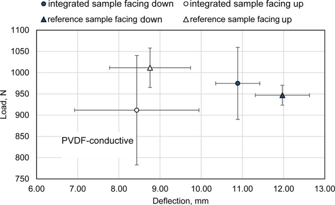
For the reference samples, even though the composition was symmetric, the manufacturing-induced defects can be considered that may induce slight unsymmetrical properties, for example, the downside of the laminate is not directly exposed to heat during curing as it is laid on the table/fixture of the oven, and heat is mainly reached via conductivity from the exposed faces of the sample. Thus, on the same principle, samples were tested faced up and samples faced down to provide a comparative study. For all samples, the load-deflection curves were extracted. Figure 16 shows typical results for the reference samples. The tests were proven consistent via providing repeatable data. For each sample, a maximal load followed by a sudden drop corresponding to the occurrence of macroscopic interlaminar delamination damage was observed (highlighted within a red circle in the figure). Data at such point are presented in Figure 17 for the integrated and referenced samples faced up and down. Facing up and down did not give any definite conclusions for the load-carrying capacity in bending as the load was higher for the faced-down integrated samples and vice versa for the reference ones. However, faced-down samples exhibited higher deflection.
Figure 16.
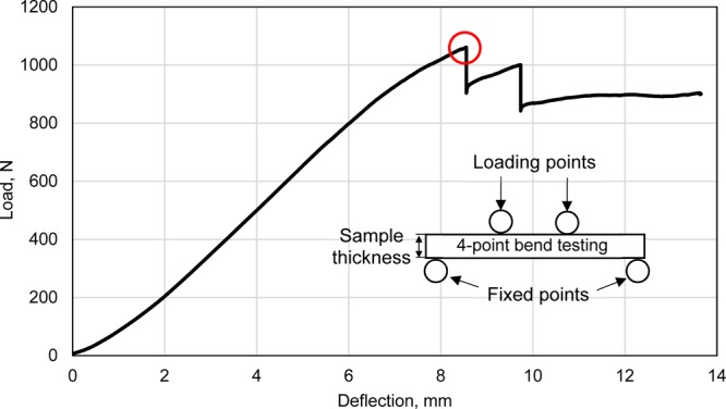
Typical four-point bending load-deflection curve for reference samples.
Figure 17.
Average load vs deflection values obtained with four-point bending test.
Even if the standard deviations are not negligible, a general tendency can be observed. The orientation of the sample seemed to significantly influence the flexural behavior. Samples facing down reached a maximal deflection around 8–9 mm, whereas samples facing up (as depicted in Figure 1) reached a higher range around 11–12 mm. This difference may be explained by the manufacturing parameters such as the aforementioned nonsymmetric curing. The unsymmetrical integrated samples with FibroTend and the conductive layer show advantageous bending properties in terms of failure load when facing down and disadvantageous ones when facing up, compared to their respective reference samples. However, whatever the side of testing (either facing up or down), the integrated samples fail at a lower deflection than that for the reference samples. Also, it can be seen that the difference of maximal deflection is more important between the integrated and reference samples when samples are facing down than when they are facing up. This attributes to the maximal strain occurring in the sample at the outer surface undergoing tensile stresses, opposite to the loading pin surface, as epoxies are more susceptible to tensile damage than compressive. However, it has been shown in the literature that sudden drop points in lateral loading (such as that in four-point bend tests) corresponds to extensive interlaminar delamination occurring between internal layers (herein composite plies).60
When the FibroTend layer was on the outer side (facing floor), this additional polymer layer associated with conductive resin played a more important role. It confirms that the FibroTend and/or the graphene–epoxy resin are a disadvantage for the laminate properties in terms of maximal deflection. This observation is supported by the visual assessment of the samples after failure. The modified samples facing floor always delaminate and break at the FibroTend layer interface.
Thus, it can be concluded that the FibroTend layer and, in particular, the conductive resin addition
decreases the maximal deflection achievable,
increases the failure load when located at the outer face (facing floor), and
decreases the failure load when located at the inner face (facing ceiling).
It can be assumed that the conductive resin plays a larger role than the FibroTend layer for decreasing the mechanical properties of the laminate. The conductive epoxy has minor mechanical strength compared to the PVDF nanofibers and its volume fraction is more important than the 0.2 gsm of FibroTend embedded. Thus, a reduction of the conductive resin quantity used for the IDE would be of interest in terms of both the IDE manufacturing as detailed in Design of the IDE Layout for Composite Integration section as well in ensuring satisfying mechanical properties. Nevertheless, because of the significant standard deviation of the results, a larger campaign of mechanical testing would be of interest to confirm these observations.
This first mechanical testing in this study allows us to raise a crucial topic: to what extend the FibroTend layer and the conductive resin play a mechanical role in the flexural toughness of the laminate: delamination, bonding, interlaminar shear, and failure propagation mode are as many points of interest for a further work. Independent of the electrical aspect of the targeted health monitoring in this study, the additional elements within the laminate must not reduce significantly the mechanical performances. If due to health monitoring, the mechanical performances of the laminates are less advantageous, their use might be questioned at the material selection step of the structure design.
6. Conclusions
This research highlights the importance of requiring new process cycles for addition of internal piezoelectric capability and conductive layers. It proposes to use a polymer system for the conductive layer (RTM6) similar to the composite (M21) to reduce material mismatch and improve bonding between the layer and plies. Raw material characterization before laminate manufacturing showed reliable and satisfying piezoelectric results for PVDF powder, Finetex, and FibroTend:
XRD and FTIR techniques gave in-agreement PVDF crystal phase,
SEM showed satisfying morphology: homogeneous shape and expected size of fiber diameter,
EDXS highlighted a carbon-based contamination level slightly higher than expected.
Regarding the manufacturing of a high-performance laminate modified with a piezoelectric FibroTend layer and a conductive resin electrode, main challenges experienced were as follows:
achieving a satisfying conductive resin mixture: homogeneous mixing, graphene safety requirements, and appropriate viscosity;
depositing conductive resin on pre-preg to form an IDE layout with similar resin: print, thickness, and accuracy; and
curing laminate without the conductive resin to flow: accuracy of the electrode layout depends on it.
Postprocessing analyses were promising:
In terms of conductive resin localization, pulsed thermography and ultrasonic C-scanning showed accurate localization. In both cases, a significant difference in thermal decay or transmittance was observed between a zone of the modified laminate with and without the conductive resin.
Graphene–epoxy resin (2 wt %) showed efficiency after curing as an electrical resistance was measured.
Four-point bending tests revealed the influence of the FibroTend layer and conductive resin on the flexural properties of the modified laminate. Compared to the reference samples, modified samples experienced a higher delamination (localized at the FibroTend layer) with lower flexural strength.
Acknowledgments
The authors would like to acknowledge the UK EPSRC funded projects, STRAINcomp (ref. no. EP/R016828/1) and CAMREG (ref. no. EP/P007805/1). The authors would also like to thank supports from FGV Cambridge Nanosystems Ltd. and Munro Technology Ltd.
The authors declare no competing financial interest.
References
- Baker A.; Gunnion A. J.; Wang J. On the Certification of Bonded Repairs to Primary Composite Aircraft Components. J. Adhes. 2015, 91, 4–38. 10.1080/00218464.2014.883315. [DOI] [Google Scholar]
- Bhanushali R.; Ayre D.; Nezhad H. Y. Tensile Response of Adhesively Bonded Composite-to-composite Single-lap Joints in the Presence of Bond Deficiency. Procedia CIRP 2017, 59, 139–143. 10.1016/j.procir.2016.09.021. [DOI] [Google Scholar]
- Yazdani Nezhad H.; Zhao Y.; Liddel P. D.; Marchante V.; Roy R. A novel process-linked assembly failure model for adhesively bonded composite structures. CIRP Ann. 2017, 66, 29–32. 10.1016/j.cirp.2017.04.103. [DOI] [Google Scholar]
- Yazdani Nezhad H.; Auffray A.; McCarthy C.; O’Higgins R.. Impact damage response of carbon fibre-reinforced aerospace composite panels. Proceedings of the 20th International Conference on Composite Materials (ICCM20), 2015.
- Fasasi A. Y.; Ngom B. D.; Kana-Kana J. B.; Bucher R.; Maaza M.; Theron C.; Buttner U. Synthesis and characterisation of Gd-doped BaTiO3 thin films prepared by laser ablation for optoelectronic applications. J. Phys. Chem. Solids 2009, 70, 1322–1329. 10.1016/j.jpcs.2009.06.022. [DOI] [Google Scholar]
- Chahal R. P.; Mahendia S.; Tomar A. K.; Kumar S. γ-Irradiated PVA/Ag nanocomposite films: Materials for optical applications. J. Alloys Compd. 2012, 538, 212–219. 10.1016/j.jallcom.2012.05.085. [DOI] [Google Scholar]
- Ahmadpoor P.; Nateri A. S.; Motaghitalab V. The optical properties of PVA/TiO2composite nanofibers. J. Appl. Polym. Sci. 2013, 130, 78–85. 10.1002/app.39147. [DOI] [Google Scholar]
- Jung C. S.; Lee I. T.; Jang P. W.; Seomoon K.; Kim K. H. Electro-optical properties of nano-thickness polymer film. J. Nanosci. Nanotechnol. 2012, 12, 3326–3329. 10.1166/jnn.2012.5604. [DOI] [PubMed] [Google Scholar]
- Zhang J.; Heitmann A. A.; Alpay S. P.; Rossetti G. A. Aspects of the Electrocaloric Behavior of Ferroelectric Thin Films: A Review of the Predictions of the Landau-Ginzburg Theory. Integr. Ferroelectr. 2011, 125, 168–175. 10.1080/10584587.2011.574486. [DOI] [Google Scholar]
- Zhou X.; Chu B.; Neese B.; Lin M.; Zhang Q. Electrical Energy Density and Discharge Characteristics of a Poly(vinylidene fluoride-chlorotrifluoroethylene)Copolymer. IEEE Trans. Dielectr. Electr. Insul. 2007, 14, 1133–1138. 10.1109/tdei.2007.4339472. [DOI] [Google Scholar]
- Kong L. B.; Zhang T. S.; Ma J.; Boey F. Progress in synthesis of ferroelectric ceramic materials via high-energy mechanochemical technique. Prog. Mater. Sci. 2008, 53, 207–322. 10.1016/j.pmatsci.2007.05.001. [DOI] [Google Scholar]
- Barber P.; Balasubramanian S.; Anguchamy Y.; Gong S.; Wibowo A.; Gao H.; Ploehn H.; Zur Loye H.-C. Polymer Composite and Nanocomposite Dielectric Materials for Pulse Power Energy Storage. Materials 2009, 2, 1697–1733. 10.3390/ma2041697. [DOI] [Google Scholar]
- Castro P.; Buchenauer C.; Gaudet J.; Schamiloglu E.. Studies of dielectric breakdown under pulsed power conditions. IEEE, Pulsed Power Conference, 2005; IEEE, 2005; pp 978–981.
- Chang J.; Dommer M.; Chang C.; Lin L. Piezoelectric nanofibers for energy scavenging applications. Nano Energy 2012, 1, 356–371. 10.1016/j.nanoen.2012.02.003. [DOI] [Google Scholar]
- Castro M.; Lu J.; Bruzaud S.; Kumar B.; Feller J.-F. Carbon nanotubes/poly(ε-caprolactone) composite vapour sensors. Carbon 2009, 47, 1930–1942. 10.1016/j.carbon.2009.03.037. [DOI] [Google Scholar]
- Castro M.; Kumar B.; Feller J. F.; Haddi Z.; Amari A.; Bouchikhi B. Novel e-nose for the discrimination of volatile organic biomarkers with an array of carbon nanotubes (CNT) conductive polymer nanocomposites (CPC) sensors. Sens. Actuators, B 2011, 159, 213–219. 10.1016/j.snb.2011.06.073. [DOI] [Google Scholar]
- Zhang Y.-C.; Dai K.; Pang H.; Luo Q.-J.; Li Z.-M.; Zhang W.-Q. Temperature and time dependence of electrical resistivity in an anisotropically conductive polymer composite with in situ conductive microfibrils. J. Appl. Polym. Sci. 2012, 124, 1808–1814. 10.1002/app.35193. [DOI] [Google Scholar]
- Rybak A.; Boiteux G.; Melis F.; Seytre G. Conductive polymer composites based on metallic nanofiller as smart materials for current limiting devices. Compos. Sci. Technol. 2010, 70, 410–416. 10.1016/j.compscitech.2009.11.019. [DOI] [Google Scholar]
- Patel I.; Siores E.; Shah T. Utilisation of smart polymers and ceramic based piezoelectric materials for scavenging wasted energy. Sens. Actuators, A 2010, 159, 213–218. 10.1016/j.sna.2010.03.022. [DOI] [Google Scholar]
- Zhou Y.; Han S.-T.; Roy V.. Nanocomposite Dielectric Materials for Organic Flexible Electronics. Nanocrystalline Materials, 2nd ed.; Elsevier, 2014; pp 195–220. [Google Scholar]
- Howells C. A. Piezoelectric energy harvesting. Energy Convers. Manage. 2009, 50, 1847–1850. 10.1016/j.enconman.2009.02.020. [DOI] [Google Scholar]
- Lebrun L.; Guyomar D.; Guiffard B.; Cottinet P.-J.; Putson C. The Characterisation of the harvesting capabilities of an electrostrictive polymer composite. Sens. Actuators, A 2009, 153, 251–257. 10.1016/j.sna.2009.05.009. [DOI] [Google Scholar]
- Jeong S.-J.; Lee D.-S.; Kim M.-S.; Im D.-H.; Kim I.-S.; Cho K.-H. Properties of piezoelectric ceramic with textured structure for energy harvesting. Ceram. Int. 2012, 38, S369–S372. 10.1016/j.ceramint.2011.05.014. [DOI] [Google Scholar]
- Kumar B.; Kim S.-W. Energy harvesting based on semiconducting piezoelectric ZnO nanostructures. Nano Energy 2012, 1, 342–355. 10.1016/j.nanoen.2012.02.001. [DOI] [Google Scholar]
- Yang B.; Yun K.-S. Piezoelectric shell structures as wearable energy harvesters for effective power generation at low-frequency movement. Sens. Actuators, A 2012, 188, 427–433. 10.1016/j.sna.2012.03.026. [DOI] [Google Scholar]
- Balachandran U.; Narayanan M.; Liu S.; Ma B. Development of Film-on-Foil Ceramic Dielectrics for Embedded Capacitors for Power Inverters in Electric Drive Vehicles. Jpn. J. Appl. Phys. 2013, 52, 05DA10. 10.7567/Jjap.52.05da10. [DOI] [Google Scholar]
- Zhou Y.; Han S.-T.; Chen X.; Wang F.; Tang Y.-B.; Roy V. A. L. An upconverted photonic nonvolatile memory. Nat. Commun. 2014, 5, 4720. 10.1038/ncomms5720. [DOI] [PubMed] [Google Scholar]
- Wolff K.; Hilleringmann U. Solution processed inverter based on zinc oxide nanoparticle thin-film transistors with poly(4-vinylphenol) gate dielectric. Solid-State Electron. 2011, 62, 110–114. 10.1016/j.sse.2011.01.046. [DOI] [Google Scholar]
- Choi M.-C.; Kim Y.; Ha C.-S. Polymers for flexible displays: From material selection to device applications. Prog. Polym. Sci. 2008, 33, 581–630. 10.1016/j.progpolymsci.2007.11.004. [DOI] [Google Scholar]
- Baeg K.-J.; Jung S.-W.; Khim D.; Kim J.; Kim D.-Y.; Koo J. B.; Quinn J. R.; Facchetti A.; You I.-K.; Noh Y.-Y. Low-voltage, high speed inkjet-printed flexible complementary polymer electronic circuits. Org. Electron. 2013, 14, 1407–1418. 10.1016/j.orgel.2012.12.022. [DOI] [Google Scholar]
- Jang J.; Song Y.; Yoo D.; Kim T.-Y.; Jung S.-H.; Hong S.; Lee J.-K.; Lee T. Micro-scale twistable organic field effect transistors and complementary inverters fabricated by orthogonal photolithography on flexible polyimide substrate. Org. Electron. 2014, 15, 2822–2829. 10.1016/j.orgel.2014.08.025. [DOI] [Google Scholar]
- Huang X.; Iizuka T.; Jiang P.; Ohki Y.; Tanaka T. Role of Interface on the Thermal Conductivity of Highly Filled Dielectric Epoxy/AlN Composites. J. Phys. Chem. C 2012, 116, 13629–13639. 10.1021/jp3026545. [DOI] [Google Scholar]
- Wang T.; Liang G.; Yuan L.; Gu A. Unique hybridized graphene and its high dielectric constant composites with enhanced frequency stability, low dielectric loss and percolation threshold. Carbon 2014, 77, 920–932. 10.1016/j.carbon.2014.06.006. [DOI] [Google Scholar]
- Kuzhir P.; Paddubskaya A.; Plyushch A.; Volynets N.; Maksimenko S.; Macutkevic J.; Kranauskaite I.; Banys J.; Ivanov E.; Kotsilkova R.; Celzard A.; Fierro V.; Zicans J.; Ivanova T.; Merijs Meri R.; Bochkov I.; Cataldo A.; Micciulla F.; Bellucci S.; Lambin P. Epoxy composites filled with high surface area-carbon fillers: Optimization of electromagnetic shielding, electrical, mechanical, and thermal properties. J. Appl. Phys. 2013, 114, 164304. 10.1063/1.4826529. [DOI] [Google Scholar]
- Di Sante R. Fibre Optic Sensors for Structural Health Monitoring of Aircraft Composite Structures: Recent Advances and Applications. Sensors 2015, 15, 18666–18713. 10.3390/s150818666. [DOI] [PMC free article] [PubMed] [Google Scholar]
- Frontini P.; Lotfian S.; Monclús M. A.; Molina-Aldareguia J. M. High Temperature Nanoindentation Response of RTM6 Epoxy Resin at Different Strain Rates. Exp. Mech. 2015, 55, 851–862. 10.1007/s11340-015-9985-4. [DOI] [Google Scholar]
- Bao X.; Chen L. Recent progress in distributed fiber optic sensors. Sensors 2012, 12, 8601–8639. 10.3390/s120708601. [DOI] [PMC free article] [PubMed] [Google Scholar]
- Ueberschlag P. PVDF piezoelectric polymer. Sens. Rev. 2001, 21, 118–126. 10.1108/02602280110388315. [DOI] [Google Scholar]
- Gusarov B.PVDF Piezoelectric Polymers: Characterization and Application to Thermal Energy Harvesting; HAL: Grenoble, 2015. [Google Scholar]
- Yen J. H.; Amin-Sanayei R.. Polyvinylidene Fluoride. Encyclopedia of Chemical Processing; Tailor & Francis: New York, 2006; Vol. 1, pp 2379–2381. [Google Scholar]
- Mohamadi S.Preparation and Characterization of PVDF/PMMA/Graphene Polymer Blend Nanocomposites by Using ATR-FTIR Technique. Infrared Spectroscopy—Materials Science, Engineering and Technology; IntechOpen, 2012; pp 213–232. [Google Scholar]
- Correia H. M. G.; Ramos M. M. D. Quantum modelling of poly(vinylidene fluoride). Comput. Mater. Sci. 2005, 33, 224–229. 10.1016/j.commatsci.2004.12.040. [DOI] [Google Scholar]
- Gomes J.; Serrado Nunes J.; Sencadas V.; Lanceros-Mendez S. Influence of the β-phase content and degree of crystallinity on the piezo- and ferroelectric properties of poly(vinylidene fluoride). Smart Materials and Structures 2010, 19, 065010. 10.1088/0964-1726/19/6/065010. [DOI] [Google Scholar]
- Salimi A.; Yousefi A. A. Analysis Method. Polym. Test. 2003, 22, 699–704. 10.1016/S0142-9418(03)00003-5. [DOI] [Google Scholar]
- HexPly M21 180°C (350°F) Curing Epoxy Matrix—Product Datasheet; Hexcel corporation, 2015.
- Knight R. R.; Mo C.; Clark W. W. MEMS interdigitated electrode pattern optimization for a unimorph piezoelectric beam. J. Electroceram. 2011, 26, 14–22. 10.1007/s10832-010-9621-8. [DOI] [Google Scholar]
- Ferrer J.; Alonso J.; de Ávila S. Electrical characterization of photodetectors based on poly(3-hexylthiophene-2,5-diyl) layers. Sensors 2014, 14, 4484–4494. 10.3390/s140304484. [DOI] [PMC free article] [PubMed] [Google Scholar]
- Tkalya E.; Ghislandi M.; Alekseev A.; Koning C.; Loos J. Latex-based concept for the preparation of graphene-based polymer nanocomposites. J. Mater. Chem. 2010, 20, 3035–3039. 10.1039/b922604d. [DOI] [Google Scholar]
- Kanik M.; Aktas O.; Sen H. S.; Durgun E.; Bayindir M. Spontaneous high piezoelectricity in poly(vinylidene fluoride) nanoribbons produced by iterative thermal size reduction technique. ACS Nano 2014, 8, 9311–9323. 10.1021/nn503269b. [DOI] [PubMed] [Google Scholar]
- Martins P.; Lopes A. C.; Lanceros-Mendez S. Electroactive phases of poly(vinylidene fluoride): Determination, processing and applications. Prog. Polym. Sci. 2014, 39, 683–706. 10.1016/j.progpolymsci.2013.07.006. [DOI] [Google Scholar]
- Ahn Y.; Lim J. Y.; Hong S. M.; Lee J.; Ha J.; Choi H. J.; Seo Y. Enhanced Piezoelectric Properties of Electrospun Poly(vinylidene fluoride)/Multiwalled Carbon Nanotube Composites Due to High β-Phase Formation in Poly(vinylidene fluoride). J. Phys. Chem. C 2013, 117, 11791–11799. 10.1021/jp4011026. [DOI] [Google Scholar]
- Kabir E.; Khatun M.; Nasrin L.; Raihan M. J.; Rahman M. Pure β-phase formation in polyvinylidene uoride (PVDF)-carbon nanotube composites. J. Phys. D: Appl. Phys. 2017, 50, 163002. 10.1088/1361-6463/aa5f85. [DOI] [Google Scholar]
- Li Y.; Xu J.-Z.; Zhu L.; Xu H.; Pan M.-W.; Zhong G.-J.; Li Z.-M. Multiple stage crystallization of gamma phase poly(vinylidene fluoride) induced by ion-dipole interaction as revealed by time-resolved FTIR and two-dimensional correlation analysis. Polymer 2014, 55, 4765–4775. 10.1016/j.polymer.2014.07.022. [DOI] [Google Scholar]
- Lanceros-Méndez S.; Mano J. F.; Costa A. M.; Schmidt V. H. FTIR and dsc studies of mechanically deformed β-pvdf films. J. Macromol. Sci., Part B: Phys. 2001, 40, 517–527. 10.1081/MB-100106174. [DOI] [Google Scholar]
- Ince-Gunduz B. S.; Alpern R.; Amare D.; Crawford J.; Dolan B.; Jones S.; Kobylarz R.; Reveley M.; Cebe P. Impact of nanosilicates on poly(vinylidene fluoride) crystal polymorphism: Part 1. Melt-crystallization at high supercooling. Polymer 2010, 51, 1485–1493. 10.1016/j.polymer.2010.01.011. [DOI] [Google Scholar]
- Ávila A. F.; Peixoto L. G. Z. d. O.; Silva Neto A.; de Ávila Junior J.; Carvalho M. G. R. Bending Investigation on Carbon Fiber/Epoxy Composites Nano-Modified by Graphene. J. Braz. Soc. Mech. Sci. Eng. 2012, 34, 269–275. 10.1590/S1678-58782012000300007. [DOI] [Google Scholar]
- Silva Neto A.; da Cruz D. T. L.; Ávila A. F. Nano-modified adhesive by graphene: the single lap-loint case. Mater. Res. 2013, 16, 592–596. 10.1590/S1516-14392013005000022. [DOI] [Google Scholar]
- Fahr A.; Kandeil A. Y.. Ultrasonic C-Scan Inspection of Composite Materials; Engineering Journal of Qatar University, 1992; Vol. 5, pp 201–222. [Google Scholar]
- ASTM-D7264/D7264M-15. Standard Test Method for Flexural Properties of Polymer Matrix Composite Materials; ASTM International: West Conshohocken, PA, 2015.
- Nezhad H. Y.; Merwick F.; Frizzell R. M.; McCarthy C. T. Numerical analysis of low-velocity rigid-body impact response of composite panels. Int. J. Crashworthiness 2015, 20, 27–43. 10.1080/13588265.2014.963378. [DOI] [Google Scholar]