Abstract
Finding the material characteristics satisfying most of the photovoltaic conditions is difficult. In contrast, utilization of foreign materials that can contribute to light harvesting and charge transfers in the devices is now desirable/thought-provoking. Herein, a binary hybrid photoanode utilizing nano-amassed micron-sized mesoporous zinc oxide hollow spheres (meso-ZnO HS) in conjunction with SnO2 nanoparticles (NPs), i.e., SnO2 NP_ZnO HS (for an optimized weight ratio (8:2)), displayed a nearly ∼4-fold increase in the efficiency (η) compared to that of bare SnO2 nanoparticle device. Enhanced device efficacy in the composite photoanode-based device can be accredited to the dual function of nano-amassed meso-ZnO HS. Nano-amassed micron-sized ZnO HS embedded in the photoanode can increase the light-harnessing capability without sacrificing the surface area as well as optical confinement of light by multiple reflections within its cavity and enhanced light-scattering effects. Electrochemical impedance spectroscopy analysis revealed an extended lifetime of electron (τe) and a higher value of Rct2 at the working electrode/dye/redox mediator interface, indicating a minimum photoinduced electron interception. The open-circuit voltage decay reveals a slower recombination kinetics of photogenerated electrons, supporting our claim that the nano-ammased meso-ZnO HS can serve as an energy barrier to the photoinjected electrons to retard the back-transfer to the electrolyte. Moreover, the improvement in the fill factors of the composite-based devices is endorsed to the facile penetration of the electrolyte through the pores of nano-amassed meso-ZnO HS, which increases the regeneration probability of oxidized dyes.
1. Introduction
Fossil fuel resources with limited reserves are diminishing at an alarming rate with the increase in global energy demand along with the danger of the release of more greenhouse gases into the atmosphere. Solar energy with high abundance promises to be an alternative clean and environmentally friendly energy resource. Over the last few decades, solar cells have been introduced as an interesting alternative to meet the increasing energy demand of the world.1,2 A dye-sensitized solar cell (DSSC), owing to its cost-effectiveness, simpler cell structure, and promising solar-to-electricity power conversion efficiency (PCE, η), has emerged as a promising candidate alternative to the traditional solid-state silicon solar cells.3 In 1991, O’Regan and Grätzel first reported a DSSC affording a ∼7.1% PCE using a TiO2- and ruthenium-based dye as a sensitizer; then, researchers have developed various photoanodic architectures, dyes, and redox mediators over the years and achieved ∼13% record PCE till date.4,5 Nevertheless, the low electron mobility through nanocrystalline TiO2 (∼0.1–1 cm2/(V s)) and the photocatalytic activity under UV radiation restrict further efficiency improvement and long-term stability of the devices.6 Numerous wide-band-gap semiconductors such as ZnO,7 SnO2,8−10 WO3,11 Nb2O5,12 SrTiO3,13 etc. have been explored as the potential photoanodic materials alternative to TiO2 in DSSCs. Among them, SnO2 and ZnO have been found to be the most appealing. SnO2, a stable, n-type semiconductor, has two distinct advantages over TiO2 in terms of higher electron mobility14 (SnO2 ∼100–200 cm2/(V s)) and wider band gap (TiO2 ∼3.2 eV, SnO2 ∼3.6 eV).15 The higher electron mobility of SnO2 promotes faster transport of photoinjected electrons to the collector electrode, i.e., fluorine-doped tin oxide (FTO),16 thus reducing the recombination probability of photoinduced electrons, whereas a higher band gap tends to create fewer oxidative holes at the valence band, minimizing the dye degradation rate, and improves long-term stability of DSSCs.17 Furthermore, SnO2 forms homojunction with the FTO substrate and thus resolves the high-contact-resistance issue originated from the heterojunction formed between other metal oxides (like TiO2 and ZnO) and FTO.18 Despite these advantages, solar cells using SnO2 as photoanodes suffer from low energy-conversion efficiency as compared to that of TiO2. The inferior photovoltaic performance of SnO2-based DSSCs can be endorsed to (i) faster electron recombination kinetics at the semiconductor/electrolyte interface and a lower open-circuit voltage (Voc) owing to the intrinsically lower conduction band (CB) edge of SnO2 as compared to that of TiO2, (ii) reduced adsorption of dyes having carboxylic acid as an anchoring group at the SnO2 surface due to the lower isoelectric point (IEP ∼4–5) of SnO2 as compared to that of TiO2 (∼6–7).19 The lower dye adsorption in turn decreases the optical density of the photoanodic film and its ability to absorb light, resulting in a lower number of photoinduced electrons, which limits the photocurrent in the devices.20 “Bare SnO2-nanoparticle (NP)-based devices made from SnO2 nanoparticles only (size ∼20 nm) with the mostly used Ru-based N719 dye rarely show power conversion efficiencies more than PCE ∼2%”.21−23 A very convenient strategy to overcome the adverse issues in the case of SnO2-based photoanode is to make composite photoanodic architectures with other wide-band-gap metal oxides such as TiO2,24 MgO,25 and ZnO.26−29 It has been seen that in the case of SnO2-based devices the composite photoanode architecture has shown substantial improvement in device performances, resulting from a reduced reverse tunneling probability of photogenerated electrons. In composite photoanode systems, it is believed that a proper combination of electronic structures of constituents (e.g., the conduction band edge, CB edge) and distribution of electron-accepting states in the conduction band is a critical factor for good device performance.30 Zinc oxide, a typical n-type semiconductor, has a higher band-edge position as compared to that of SnO2 with a band gap of ∼3.37 eV and has the distribution of electron-accepting states in the conduction bands similar to that of SnO2, i.e., the s-orbital.31,32 Moreover, zinc oxide is less acidic as compared with SnO2 (ZnO: IEP ∼9, SnO2: IEP ∼4–5)) and can achieve diverse morphologies with high crystallinity,33−36 making it a suitable candidate for a composite mixture photoanode for SnO2-based DSSCs. Apart from the electronic properties, efficient light harvesting is an essential property for a well-performing photoanode.37 Conventional photoanodes utilizing only small-sized (approximate diameter ∼20 nm) metal oxide nanoparticles (NPs) ensure a large interfacial surface area for adsorption of dye but suffer from a significant optical loss owing to high transparency of the photoanodic film, resulting in poorer photovoltaic performance.38,39 Additionally, incorporation of light-scattering materials can boost the power conversion efficiency (PCE) in DSSCs by increasing the light-harnessing ability of the photoanode films.40 According to Mie theory, micron- or sub-micron-sized scattering centers can effectively scatter light and enhance the optical path length of the incident light in the devices, thus increasing their probability to be trapped and eventually absorbed, boosting the photogenerated current as well as the PCE.41,42 The basic platform for sensitizer adsorption is formed by blending these materials and nanoparticles together in a mixture structure.43 Unfortunately, large-sized scattering materials furnish very low surface area, resulting in a reduction in the dye adsorption, thus limiting the device efficiency.44 On the contrary, hierarchical spherical structures used as light-scattering centers can improve the light-harnessing efficiency of the photoanodes without sacrificing the specific surface area of the photoanodic films. A micrometer- or sub-micrometer-sized structure formed by assembly of nanoparticles can ensure a high specific surface area, whereas the larger-sized spherical assemblies can boost the light-harnessing efficacy via the effective scattering from a single moiety as well as from the blend. Optical confinement of incoming photons inside the photoanode film upsurges the probability of light absorption by the sensitizer, thereby increasing the number of photoinduced electrons and thus improving the device performance.45−48 However, solid particles, although provide a good scattering capacity, unfortunately inhibit diffusion of electrolyte. Intentionally created sub-micron-sized voids in the photoanode have shown significant enhancement in the device performance owing to better light scattering as well as electrolyte diffusion to regenerate the photo-oxidized sensitizer molecule, thus preventing recombination pathways at the interfaces.49,50 On the other hand, hollow spheres (HSs) can effectively increase light harvesting via light trapping within the cavity and scattering from the ensemble as well as provide accessible pores that assist the penetration of the liquid electrolyte to regenerate the sensitizer.51−56
In this context, herein, we demonstrate the bifunctional effect of nano-amassed micron-sized ZnO hollow spheres loading on SnO2 photovoltaic. Nano-amassed micron-sized meso-ZnO hollow spheres provide a high surface area with better light-harvesting ability owing to their mesoporous nature and hollow architecture. Moreover, ZnO hollow spheres provide pathways for infiltration of liquid electrolyte responsible for regeneration of sensitizer and simultaneously act as a partial energy barrier owing to the high conduction band position in reducing the reverse tunneling probability of photoinduced electrons at the semiconductor/sensitizer/electrolyte interface. A systematic study was performed on the effect of nano-amassed meso-ZnO hollow spheres in improving photovoltaic performances and in optimizing the loading of ZnO hollow spheres by varying the amount of ZnO hollow spheres in different ratios, which advocates the function of ZnO hollow spheres as an efficient synergy booster in photovoltaic performances and as an efficient light-scattering material, as well as a partial energy barrier impeding the back-recombination processes.
2. Experimental Section
2.1. Materials Used
All of the chemicals were used for the experiments without further purification. SnCl2·2H2O power (Merck), terpineol (Himedia), poly(ethylene glycol) (PEG)–poly(propylene glycol) (PPG)–PEG triblock copolymer (Aldrich), SnCl4·5H2O (Aldrich), 2-methoxy ethanol (Himedia), absolute ethanol (TMEDA), acetylacetone (Merck), 4-tert-butylpyridine (Himedia), hexachloroplatinic acid (H2PtCl6, Aldrich), Zn(NO3)2·6H2O (Aldrich), di-tetrabutylammonium cis-bis(isothiocyanato)bis(2,2′-bipyridyl-4,4′-dicarboxylato)ruthenium(II) (Dyesol, Australia), ethanol (EtOH), CH3CN (Merck), PEG 200 (Merck), valeronitrile (Sigma-Aldrich), tert-butanol (Merck) were used. Fluorine-doped tin oxide (resistivity ∼13–15 Ω/sq cm, Aldrich), and poly(tetrafluoroethylene) filter (0.2 μm, Axiva) were purchased. High-grade Milli-Q water (18.2 MΩ cm) was used for all of the experiments.
2.2. Synthesis of SnO2 Nanoparticles (SnO2 NP)
SnO2 nanoparticles were prepared by adopting a reported protocol.57 In the synthetic procedure, first, 5 mmol of SnCl2·2H2O (AR) is dissolved in 50 mL of EtOH followed by stirring for 30 min. In a 250 mL, round-bottom (RB), two-necked flask, 50 mL of distilled H2O was added and kept at 100 °C with a water-cooled condenser at one end and a dropping funnel at the other. Then, the prepared SnCl2 solution was added slowly to the 250 mL flask containing 50 mL water through a dropping funnel under vigorous stirring and the system was kept at 100 °C for 12 h with continuous stirring. The resultant product was centrifuged and washed with distilled H2O and EtOH 2–3 times and dried at 60 °C in an oven. Finally, the powder was calcined at 500 °C for 1 h to obtain the final products for further characterizations.
2.3. Synthesis of Nano-Amassed Mesoporous Hollow ZnO Microspheres (Meso-ZnO HS)
Mesoporous hollow ZnO microspheres have been synthesized using a one-step reflux route following a reported protocol.58 Typically, 2.973 g of zinc nitrate hexahydrate was dissolved in 100 mL of PEG 200 under stirring conditions. The resulting solution was then transferred into a 250 mL RB flask and progressively heated to 160 °C. The system was kept for 6 h under a refluxing process and then allowed to cool naturally. The products were collected by centrifugation, washed with absolute EtOH and distilled H2O several times, and kept at 60 °C for drying. Finally, the brown powders were subjected to calcination for 4 h at 500 °C in a muffle furnace to get the final products.
2.4. Preparation of SnO2 NP–ZnO HS (SZx, x = 10, 20, 30) Composites
The SnO2 NP_ZnO HS composites were prepared by sonochemical treatment taking the desired amount of ZnO HS and SnO2 NP in different ratios (SnO2 NP/ZnO HS 9:1, 8:2, and 7:3; named SZ10, SZ20, and SZ30 hereafter). In detail, to form 1 g of SZ10, i.e., the SnO2 NP/ZnO HS (9:1) composite, 0.1 g of as-synthesized ZnO HS was dispersed in isopropanol under ultrasonic treatment for 30 min. Then, the rest of the amount (0.9 g) of SnO2 NP was added into the dispersed solution followed by further ultrasonication for another 30 min. The similar procedure was followed for the rest of the composites with appropriate amounts of SnO2 NP and ZnO HS. The final composite products were obtained by placing the dispersed solutions inside an oven to evaporate the solvent.
2.5. Device Fabrication
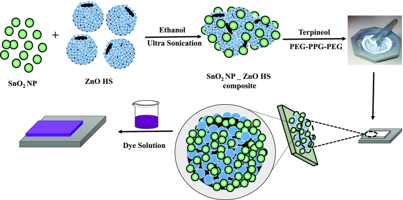
All of the photoanodes were fabricated by making a homogeneous paste of SnO2 NP and SnO2 NP–ZnO HS composite, viz., SZ10, SZ20, SZ30, following a procedure similar to that in our previous report.59 First, a solution of 0.2 M SnCl4·5H2O in 2-methoxy ethanol was spin-coated onto precleaned FTO and calcined at 500 °C to get a SnO2 compact layer.60 For the preparation of homogeneous pastes, 0.5 g of SnO2 NP or SnO2 NP_ZnO HS composites, viz., SZ10, SZ20, SZ30, was ground with a mixture of acetic acid (0.05 mL), acetylacetone (0.1 mL), terpineol, and PEG–PPG–PEG in a mortar–pestle. This homogeneous paste was applied using the doctor blade technique, dried at 120 °C, and finally calcined at 500 °C for 1/2 h. The pictorial representation of the step-by-step fabrication of photoanode is depicted in Scheme 1. The thickness of the photoanode layers was measured by a surface profilometer and found to be ∼13–15 μm (thicknesses of champion devices are provided in Table 1). After the sensitization process with N719 dye for 8 h, photoanodes were sandwiched with the Pt counter electrode (CE) using a spacer between the electrodes, and addition of I–/I3– electrolyte solution completed the device fabrication. The device active area was set to be 0.16 cm2 for all the devices.
Scheme 1. Pictorial Representation of Hybrid Photoanode Preparation.
Table 1. Photovoltaic Performance Parameters for DSSCs Composed of Photoanodes Based on SnO2 NPs and NP_ZnO HS Compositesa.
| DSSC photoanode | thickness of the best-performed photoanodes (μm) | Jsc (mA/cm2) | Voc (mV) | FF (%) | PCE (η, %) | IPCEmax (%) |
|---|---|---|---|---|---|---|
| SnO2 NP | 13.94 | 7.82 (±0.5) | 383.4 (±4) | 35.1 (±1.9) | 1.15 | 46 |
| SnO2 NP_ZnO HS (9:1) | 14.10 | 9.58 (±0.4) | 612.3 (±7) | 56.1 (±2.1) | 3.29 | 56 |
| SnO2 NP_ZnO HS (8:2) | 13.89 | 11.01 (±0.6) | 632.3 (±6) | 62.8 (±2.5) | 4.37 | 62 |
| SnO2 NP_ZnO HS (7:3) | 13.71 | 8.89 (±0.5) | 638.2 (±8) | 64.6 (±3.1) | 3.67 | 52 |
Data reported for the best-performed devices out of five identical devices. The average errors estimated for five devices are included. Thicknesses of the devices were found to be within the range of reference device as measured by a profilometer. The best performed device among all combinations shown in bold.
2.6. Characterization and Measurements
Crystallinity and phase characterization were carried out using a Bruker D8 Advance X-ray diffractometer (30 kV and 30 mA, Cu Kα source (α = 0.154 nm)). The UV–vis diffused reflectance spectroscopic (DRS) analysis was carried out using JASCO model V-650. The studies on the morphology of the photoanodic materials and elemental analysis were carried out by field emission scanning electron microscopy (FESEM) using a Zeiss (model: Sigma) instrument (for FESEM, ∼2–5 kV and for energy-dispersive X-ray (EDX), ∼20 kV). A Horiba LabRAM HR spectrometer was used for Raman analysis. Brunauer–Emmett–Teller (BET) analysis was performed in a Beckman–Coulter SA 3100 N2 adsorption apparatus (samples were degassed at 200 °C for 4 h). Transmission electron microscopy (TEM) analysis was carried out using JEOL JEM 2100 F. The thickness of the deposited films onto FTO substrates was measured using a surface profilometer (Veeco Dektak-150). Incident photon-to-current conversion efficiency (IPCE) measurements were performed in Newport Oriel IQE-200. Electrochemical impedance spectroscopic (EIS) analysis was conducted in CHI660E. A Newport ORIEL Sol3A solar simulator and a digital source meter (Keithley 2400) was used to evaluate photovoltaic performance.
3. Results and Discussion
3.1. Powder X-ray Diffraction (PXRD) Analysis
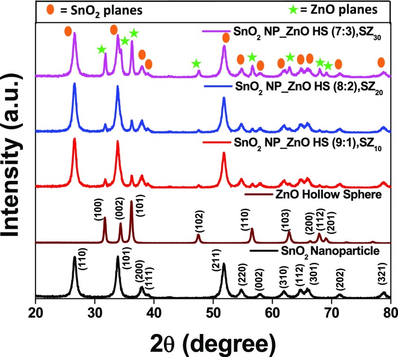
Powder X-ray diffraction (PXRD) patterns were recorded to confirm the phase purity and crystallinity of pristine SnO2 nanoparticle, ZnO HS, and SnO2_ZnO HS composites, viz., SZ10, SZ20, and SZ30, as shown in Figure 1. All of the diffraction peaks from lattice planes (110), (101), (200), (111), (211), (220), (002), (310), (112), (301), (202), and (321) confirm the tetragonal phase (JCPDS file card no. 41-1445) of SnO2 NP with a = b = 0.474 nm and c = 0.317 nm. The average crystallite sizes of the nanoparticles were evaluated using the Scherrer equation61 from the full width at half-maxima of the (110) peak of SnO2 and is found to be ∼11.40 nm. In the case of ZnO HS, (100), (002), (101), (102), (110), (103), (112), and (201) peaks were indexed to the wurtzite phase (JCPDS file card no. 36-1451) of ZnO with no traceable impurity peaks.
Figure 1.
Powder XRD patterns for the SnO2 nanoparticle film (SnO2 NP, black line), SnO2 NP_ZnO HS (9:1), SZ10 (red line); SnO2 NP_ZnO HS (8:2), SZ20 (blue line); and SnO2 NP_ZnO HS (7:3), SZ30 (magenta line) films on glass substrates.
Notably, the recorded PXRD patterns for composites SZ10, SZ20, and SZ30 show the diffraction peaks assignable to the wurtzite phase of the ZnO crystal as well as the tetragonal phase of SnO2 and no other additional impurity peaks were observed. It has been seen that with an increase in ZnO content the intensity of ZnO peaks also becomes prominent. To examine any change in the average crystallite size of the SnO2 nanoparticle upon ZnO hollow sphere loading, the average crystallite sizes of composites SZ10, SZ20, SZ30 were calculated monitoring the (110) lattice plane of SnO2 NP. However, it was observed that 10, 20, and 30% loading of ZnO HS did not alter the crystallite size of SnO2 NP significantly (SnO2 NP ∼11.40 nm, SZ10 ∼11.40 nm, SZ20 ∼11.39 nm, SZ30 ∼11.65 nm), which indicates that crystallinity of SnO2 NP is retained even after loading of ZnO HS.
3.2. Raman Analysis
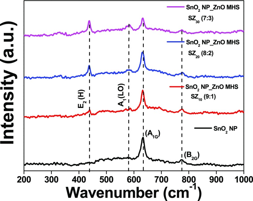
Raman spectroscopy is used to investigate the vibrational characteristics of materials and to identify the crystallization and structural defect. Figure 2 shows the typical Raman spectra of photoanodes fabricated with SnO2 nanoparticles and SnO2 NP_ZnO HS composites, viz., SZ10, SZ20, SZ30, at room temperature. For SnO2 nanoparticle samples, a sharp and dominant peak observed at 633 cm–1 is assigned to the A1g vibrational mode and the peak observed at 773 cm–1 is assigned to the B2g vibrational mode of tetragonal SnO2 lattice. A1g (633 cm–1) and B2g (771 cm–1 ) are related to the symmetric and antisymmetric stretching modes of the Sn–O bond, respectively.62 In the case of the composite samples SZ10, SZ20, and SZ30, the Raman spectra displayed the presence of both metal oxides, giving evidence of the composite nature of the mixtures. In the case of composite SZ10, along with the signature peaks of the SnO2 nanoparticle, a sharp and dominant peak was observed at 438 cm–1, assigned to the E2 (high) mode of the wurtzite hexagonal ZnO lattice. This mode is a fingerprint of the hexagonal wurtzite ZnO associated with oxygen displacement.63 Another suppressed peak at 582 cm–1 is ascribed to the A1 (LO) mode, probably occurred due to oxygen vacancy.64 As can be seen from the spectra, with the increase in ZnO content from SZ10 to SZ30 the peak intensities of the corresponding vibrations of the ZnO lattice also increase. It is observed that upon ZnO HS addition there was no shift in peak positions of the tetragonal SnO2 lattice as well as no peaks for any tertiary phases or impurity occurred, corroborating the powder XRD data.
Figure 2.
Raman spectra of the SnO2 nanoparticle film (black line), SnO2 NP_ZnO HS (9:1), SZ10 (red line); SnO2 NP_ZnO HS (8:2), SZ20 (blue line); and SnO2 NP_ZnO HS (7:3), SZ30 (magenta line), all on glass substrates.
3.3. Material Morphology
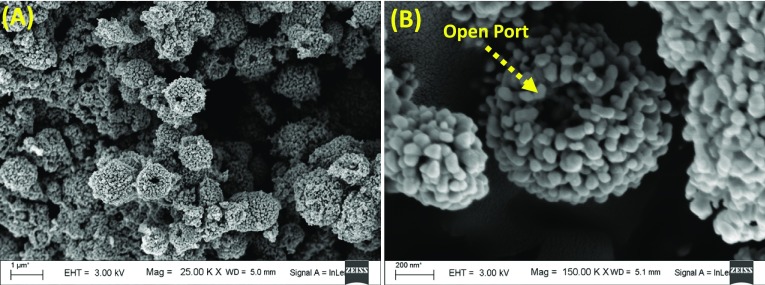
The morphological features of the as-synthesized materials and photoanodes were studied by carrying out FESEM analysis. FESEM images of as-synthesized meso-ZnO HS depicted in Figure 3A corroborate that ZnO hollow spheres have an average size of ∼1 μm. From the FESEM image, Figure 3B, it is clearly evident that as-synthesized hollow spheres are composed of self-assembled small ZnO nanoparticles with a diameter of ∼30–50 nm. The ZnO hollow spheres are formed by polymer-assisted Ostwald ripening of single-crystalline ZnO nanoparticles.58 The hollow nature of the micron-sized material favors trapping of light within the cavity as well as efficient light scattering in the photoanode while nanoparticles provide a comparably higher surface area than solid structures for efficient dye loading. The magnified image of ZnO hollow spheres endorses its porous nature and uniformly distributed pores within the hollow spheres to facilitate the penetration of electrolyte along the material to regenerate the oxidized dye, which is a critical factor in the performance of a photovoltaic device.51
Figure 3.
(A) FESEM image of as-synthesized ZnO hollow spheres and (B) magnified FESEM image of ZnO hollow spheres.
The detailed top-view and cross-sectional FESEM images of fabricated SnO2 NP and SnO2 NP_ZnO HS (8:2), SZ20, photoanode (best device performance) have been depicted in Figures S1–S3 at different magnifications. It can be clearly seen from the cross-sectional image (Figure S2) that the overall thickness of the fabricated film is ∼13–15 μm (as seen in profilometer measurements), and it shows evenly distributed ZnO HS throughout the region. From the top view of the FESEM image of the photoanode, it is seen that ZnO HS are well distributed throughout the specified region, and the hollow architecture of ZnO HS can be seen from the magnified FESEM images (trace (D) Figure S3) that facilitates the penetration of electrolyte efficiently.
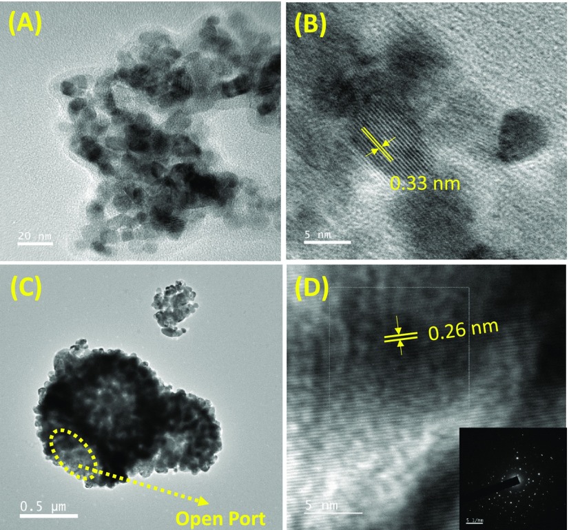
Figure 4 represents the TEM images of as-synthesized SnO2 nanoparticles and meso-ZnO hollow spheres after ultrasonication for 1.5 h in ethanol. The average size of SnO2 nanoparticles in Figure 4A is found to be ∼10 nm. Figure 4B shows the HRTEM image of SnO2 nanoparticles with a well-defined lattice pattern, revealing their crystalline nature, a prerequisite for the efficient photoinjected charge migration. The SnO2 nanoparticles exhibit lattice fringes with an interplanar distance (d-spacing) of 0.33 nm that can be indexed as the (110) plane, as shown in the HRTEM image. TEM images (Figures 4C and S4) of the as-synthesized meso-ZnO hollow sphere sample clearly show the micrometer size range of the samples in accordance with FESEM analysis. It can be seen from the TEM image that the meso-ZnO hollow sphere is composed of interconnected smaller ZnO nanoparticles (average size ranging from ∼30 to 50 nm) that assembled into a hollow morphology and showed excellent porosity. As a result, light can be trapped inside the hollow cavity (through open port in trace (C)) by multiple reflections as well as enhances the light-harnessing ability of the photoanode. Trace (D) depicts the HRTEM image of nano building blocks of meso-ZnO HS showing an interplanar distance of d ∼0.26 nm, corresponding to the (100) plane. The selected-area electron diffraction (SAED) pattern for meso-ZnO HS (inset to trace (D)) infers the single-crystalline nature of the wurtzite ZnO crystalline structure. The single-crystalline nano building blocks in the meso-ZnO HS microstructure are responsible for better charge transport as well as provide high surface area for adsorption of sensitizer.
Figure 4.
(A) TEM image of the as-synthesized SnO2 nanoparticle. Trace (B) represents the HRTEM image of SnO2 nanoparticles displaying growth along the lattice plane (110). (C) TEM image of as-synthesized ZnO hollow spheres. Trace (D) depicts high-resolution TEM image of meso-ZnO HS. the inset shows the SAED pattern of ZnO HS.
3.4. BET Analysis
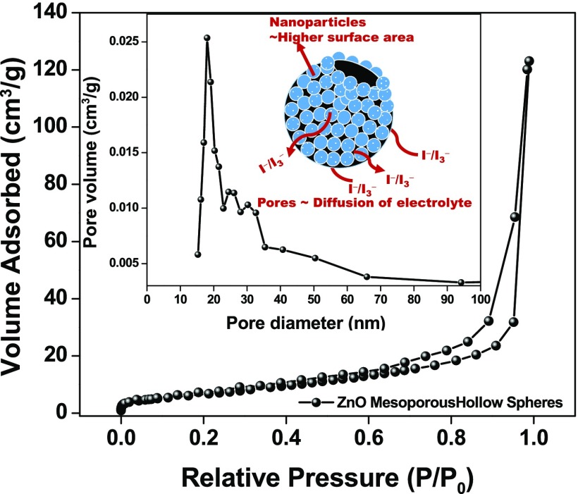
The surface area and porous structure are the key factors for the photoanodic material in DSSCs. The porous structure favors light trapping and facilitates electrolyte penetration while the later tends to increase the dye adsorption, providing a higher number of species accountable for photogenerated electrons and thus increases the photocurrent.47 The porous structure and pore size distribution of the as-prepared ZnO hollow spheres are investigated by performing the Brunauer–Emmett–Teller (BET) measurement. As shown in Figure 5, the N2 physisorption isotherm exhibits H3 hysteresis and type IV isotherm loops according to the Brunauer–Deming–Deming–Teller classification, confirming the mesoporous nature of ZnO HS, a prerequisite for DSSC applications.65,66 The BET surface area of the ZnO HS was observed to be ∼40.3 m2/g. The Barrett–Joyner–Halenda (BJH) pore size distribution curve shows the uniformly distributed pores of ∼15 nm, as can be seen from FESEM analysis. Owing to the mesoporous nature and high surface area, meso-ZnO HS can offer sufficient adsorption sites for the dye and also the electrolyte can easily be infiltrated for dye regeneration, which is limited in the case of solid hierarchical structures, as depicted in the schematic (inset to Figure 5). However, the BET surface area for a SnO2 nanoparticle is found to be 46.5 m2/g (Figure S5).
Figure 5.
Nitrogen adsorption–desorption isotherms for meso-ZnO hollow spheres. The inset shows the BJH pore size distribution plot for meso-ZnO hollow spheres, and the schematic depicts electrolyte diffusion pathways through the pores.
3.5. UV–Vis Diffused Reflectance Analysis
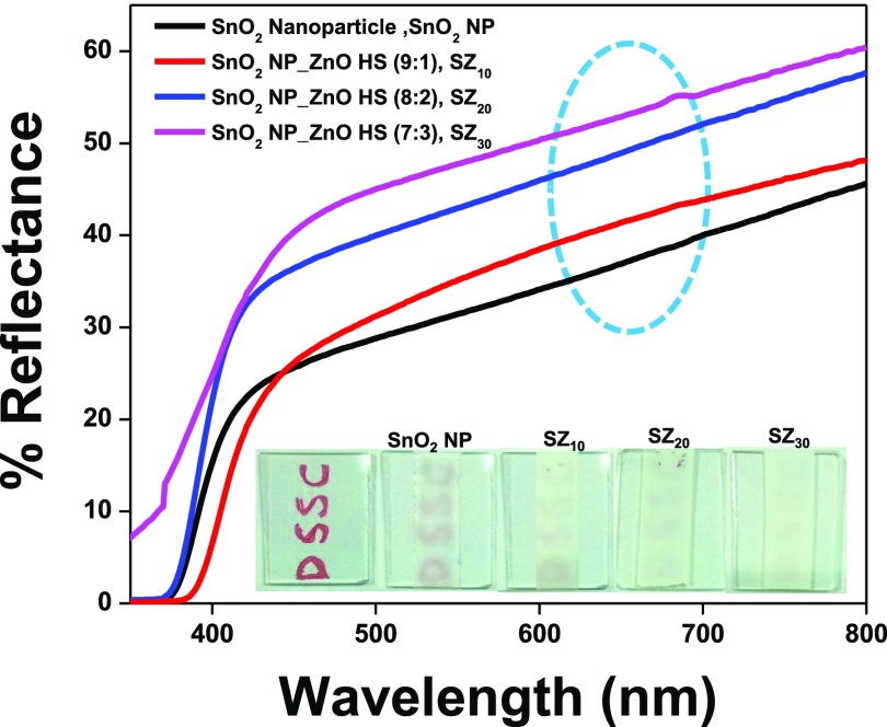
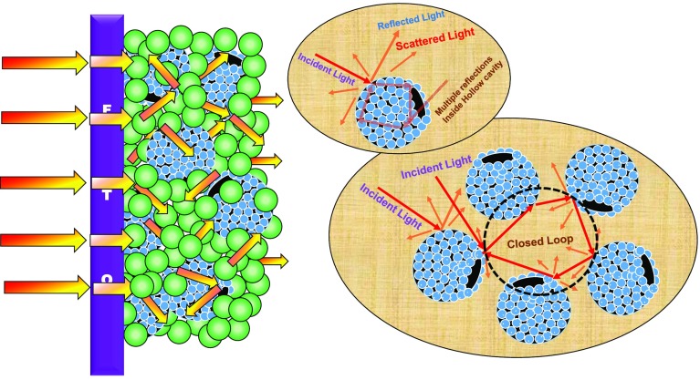
UV–vis DRS analysis of photoanode films based on pristine SnO2 NP (black line), SZ10 (red line), SZ20 (blue line), and SZ30 (magenta line) deposited on glass substrates prior to dye sensitization is shown in Figure 6. The composite photoanodic film SZ10, containing 10% ZnO HS, shows higher diffused reflectance than the pristine SnO2 film due to enhanced scattering and reflection of the incident light within the interior cavity of the hollow structure, enhancing scattering in between hollow spheres and from the ensemble as well.67 The diffused reflectance further increases with the increase in ZnO HS content, and the composite with 30% ZnO HS (SZ30) exhibits the highest reflectance among all of the photoanodes in the wavelength range 600–800 nm. EDX mapping analysis as shown in Figure S7 depicts that meso-ZnO hollow spheres are distributed homogeneously in the photoanode composite (SZ20), contributing to the effective light harvesting through trapping of light. Pictorial representation of various light-scattering pathways in the hybrid photoanode has been depicted in Scheme 2. The inset to Figure 6 depicts the digital images of different photoanodes fabricated using SnO2 nanoparticles, SZ10, SZ20, and SZ30. It has been observed that although the SZ30 photoanode shows the highest reflectance, but at the same time, the opaqueness of the photoanodic film increases with an increase in the concentration of micron-sized meso-ZnO HS, thus preventing the penetration of incident light, causing adverse effect on the photovoltaic performance. Moreover, back-scattered light at the FTO junction will cause hindrance to light penetration on increasing ZnO HS concentration.
Figure 6.
Ultraviolet–visible DRS of photoanodes SnO2 NP film (black line), SnO2 NP_ZnO HS (9:1), SZ10 (red line); SnO2 NP_ZnO HS (8:2), SZ20 (blue line); and SnO2 NP_ZnO HS (7:3), SZ30 (magenta line) on FTO. The inset depicts the digital images of fabricated photoanodes with SnO2 NP, SZ10, SZ20, and SZ30 and a blank FTO for comparison.
Scheme 2. Light Scattering Pathways in the Composite Photoanode.
Note that incoming photon flux undergoes multiple reflections within the hollow cavity of meso-ZnO HS as well as from the ensemble, thereby increasing the optical path length. Please note that the light-scattering pathways shown here are relative representations only.
3.6. Photovoltaic Performance
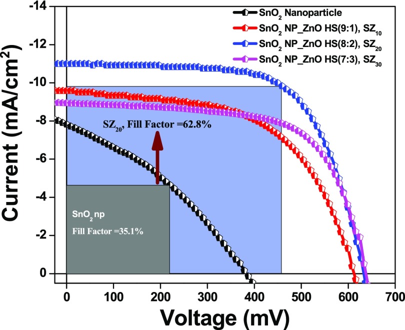
To explore the potential of hybrid photoanodes in harnessing solar energy, photovoltaic performance of the fabricated SnO2 NP as well as composite SZ10-, SZ20-, and SZ30-based devices was evaluated and photovoltaic parameters, viz., current density (Jsc), open-circuit voltage (Voc), fill factor (FF), and PCE, are summarized in Table 1.
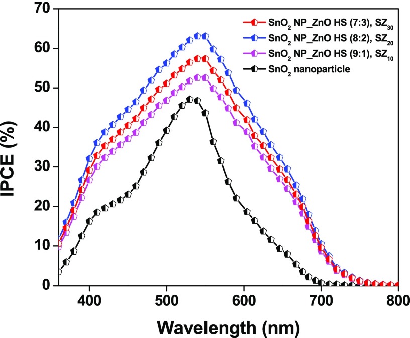
From Figure 7, it is seen that the photovoltaic device with pristine SnO2 nanoparticles exhibited a Jsc ≈ 7.82 mA/cm2, Voc ≈ 384 mV, and FF ≈ 35%, affording a PCE ≈ 1.15%. On the other hand, ZnO hollow sphere-loaded SnO2 NP composite-based devices, viz., SZ10, afforded a PCE ≈ 3.29% with Jsc ≈ 9.58 mA/cm2, Voc ≈ 612 mV, and FF ≈ 56% and SZ20 afforded a PCE ≈ 4.37% with Jsc ≈ 11.01 mA/cm2, Voc ≈ 632 mV, and FF ≈ 63%, whereas the device with 30% ZnO HS, SZ30, showed lower performance, yielding Jsc ≈ 8.89 mA/cm2, Voc ≈ 638 mV, FF ≈ 64.6%, and PCE ≈ 3.67%. The increase in the device efficacy, i.e., for SZ10 and SZ20, is mainly accredited to the increase in Jsc and Voc. The enhanced Jsc in the case of composite photoanodes SZ10 and SZ20 is due to better light-harnessing capacity of photoanodes with nano-amassed micron-sized meso-ZnO HS and a reduced recombination of photoinjected electrons at the semiconductor/electrolyte interface. From the chemisorption analysis (Table S2), it is seen that there is a slight increase in the dye loading capacity of the composite photoanode, which may be due to the comparable surface area and higher IEP value of nano-amassed meso-ZnO HS. Hence, the light harvesting in the case of hybrid photoanodes is solely due to the enhanced light reflection/scattering properties of the composite photoanodes, thereby allowing trapping of the incident light within their cavity and increasing the optical path of incident light by scattering phenomenon promoting interaction between incident photons and the dye molecules. The enhanced light scattering by the meso-ZnO hollow spheres as well as multiple reflections within the ensemble increases the possibility of harvesting the incident light, eventually absorbed by the dye molecule, and in return boosting the photogenerated current, i.e., Jsc. Second, the inhibited back-recombination of photogenerated electrons imposed by the higher conduction band level of ZnO as compared to that of SnO2 also adds to the increase in Jsc. The lower value of Voc shown by SnO2 NP-based devices is due to faster recombination of photogenerated electrons from the conduction band (CB) of SnO2 nanoparticles to the redox mediator, resulting from the reactive low-energy trap states of SnO2. However, in the case of composite photoanodes, we observed a dramatic increase in the open-circuit potential or Voc (Table 1). Voc of a DSSC device is defined as the difference between the redox potential of the redox shuttle and the Fermi energy level of the metal oxide semiconductor, and the increase in the Voc in the case of SZx (x = 10–30%) devices can be attributed to the shift of the conduction band edge of SnO2 on addition of ZnO, resulting in a higher quasi-Fermi level as well as inhibited reverse tunneling of photogenerated electrons from the CB of SnO2. A decrease in the chemical capacitance of SnO2 results in a decrease in the combined capacitance of the mixed electrode, thus shifting the CB position toward the vacuum level.68 On the other hand, a significant increase in the fill factor (FF) from ∼35% (SnO2 nanoparticle) to ∼56% (SZ10) and to ∼65% (SZ30) in the case of composite photoanode devices has been observed. An increase in the fill factor with the introduction of meso-ZnO HS can be ascribed to the higher CB position of meso-ZnO HS, which serves as a thermodynamic energy barrier for minimum photoinduced electron interception, thereby increasing the efficiency,69,70 whereas the pores of meso-ZnO HS provide a pathway for regeneration of dye in the respective layers by the redox couple.71 Although the scattering ability of photoanode SZ30 is more as compared to that of the other composite photoanodes, an increase in the concentration of ZnO HS from 20 to 30% results in deterioration of device performances. This decrease in the device performance can be attributed to the increased opaqueness of the photoanode, thus hindering the light penetration; as a result, the overall photovoltaic performance decreased. With the increase in the amount of nano-amassed meso-ZnO HS, the amount of back-scattered light also increases, leading to a lower light-absorption ability. To estimate the photocurrent features of the DSSCs, photocurrent action spectra of the DSSCs are recorded against a wavelength range of 360–800 nm. In principle, the IPCE characteristic of a photovoltaic device depends upon (i) the light-harvesting efficiency of the photoanode, (ii) the quantum yield of photoinduced electron injection, and (iii) the efficiency of collecting these injected electrons.72Figure 8 displays photosensitization in the whole visible region achieved by the dye with maximum IPCE values of ∼46, ∼56, ∼62, and ∼52% at ∼525 nm for the devices based on SnO2 nanoparticles, SZ10, SZ20, and SZ30, respectively. The higher IPCE values at a longer wavelength observed in the IPCE spectra in the case of composite photoanodes, viz., SZ10, SZ20, and SZ30, depict an enhanced light-harvesting and scattering ability of micron-sized ZnO HS, which adds to increase the overall PCE of the devices. The better light-harnessing ability is accredited to the efficient sensitization of photoanodes with meso-ZnO hollow spheres and light confinement within the photoanodes of composite devices owing to the hollow architecture as well as light-scattering ability of meso-ZnO HS. These features lead to the enhanced absorption of solar light and an increase in the quantum yield of photogenerated electron injection in the composite devices. Furthermore, the efficient regeneration of the oxidized dye molecule by the electrolyte, due to the facilitated electrolyte diffusion through the pores of meso-ZnO HS in the photoanodes, reduces the recombination rate and increases the charge collection, thus improving the IPCE. From the EDS mapping in Figure S7, it is clearly seen that nano-amassed meso-ZnO HS are homogeneously distributed throughout the specified region, leading to better light trapping and scattering, resulting in a higher light-harnessing ability as compared to that of the pristine SnO2 nanoparticle-based photoanode. The decreased IPCE value in the case of SZ30 as compared to that in SZ20 is due to higher back-scattering by micron-sized meso-ZnO HS at the FTO junction as well as increased opaqueness of the photoanodic film device resulting in a reduced charge collection efficacy (as can be seen in inset to Figure 6).
Figure 7.
J–V plots for DSSCs with the SnO2 nanoparticle film (black line), SnO2 NP_ZnO HS (9:1), SZ10 (red line); SnO2 NP_ZnO HS (8:2), SZ20 (blue line); and SnO2 NP_ZnO HS (7:3), SZ30 (magenta line) photoanodes.
Figure 8.
IPCE plots for the fabricated DSSCs composed of photoanodes based on the SnO2 nanoparticle film (black line), SnO2 NP_ZnO HS (9:1), SZ10 (red line); SnO2 NP_ZnO HS (8:2), SZ20 (blue line); and SnO2 NP_ZnO HS (7:3), SZ30 (magenta line).
3.7. EIS Analysis
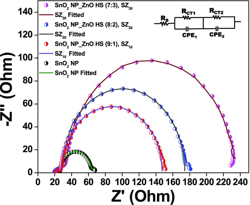
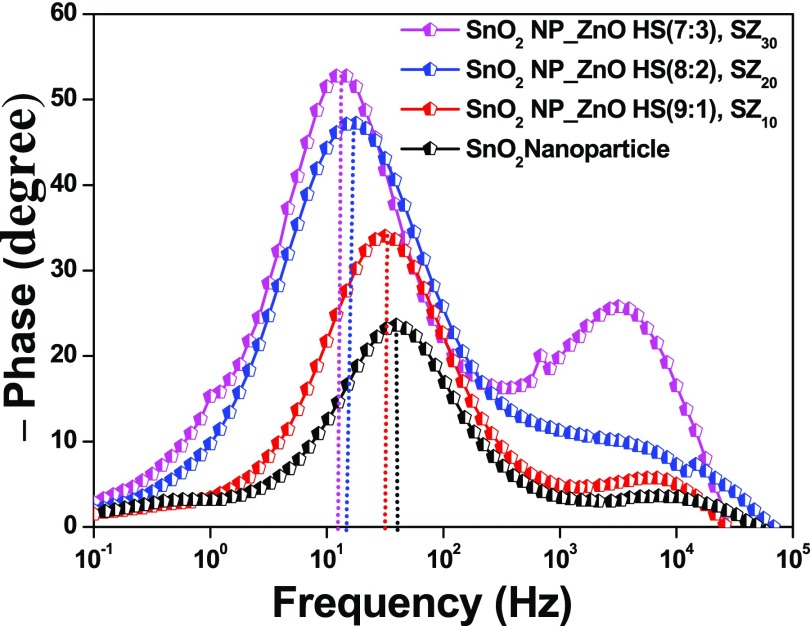
Electron transport kinetics and energetics of interfacial recombination in fabricated bare as well as composite based DSSCs have been investigated by carrying out EIS measurements for the best-performing devices in a frequency range of 0.1 Hz to 100 kHz under dark conditions at an external bias equivalent to Voc, as shown in Figures 9 and 10, and the fitting data are given in Table 2. EIS for the DSSCs typically explicates the characteristic charge transfers occurring at various interfaces in different frequency regions, viz., at the CE/electrolyte interface (1–100 kHz) and at the semiconductor/electrolyte interface (0.1–1 kHz), and the diffusion of electrolyte (0.1–0.01 kHz).59,73
Figure 9.
Nyquist plots for the fabricated DSSCs composed of SnO2 nanoparticle film (black line), SnO2 NP_ZnO HS (9:1), SZ10 (red line); SnO2 NP_ZnO HS (8:2), SZ20 (blue line); and SnO2 NP_ZnO HS (7:3), SZ30 (magenta line) devices. The inset represents the equivalent circuit diagram.
Figure 10.
Bode phase plots for the fabricated DSSCs composed of photoanodes based on the SnO2 nanoparticle film (black line), SnO2 NP_ZnO HS (9:1), SZ10 (red line); SnO2 NP_ZnO HS (8:2), SZ20 (blue line); and SnO2 NP_ZnO HS (7:3), SZ30 (magenta line).
Table 2. Fitting Parameters of EIS Analysis for the Fabricated Devices Obtained from EIS Analysis (aNyquist and bBode Plot)a.
| DSSC photoanode | Rsa (Ω) | Rct2a (Ω) | fpb (Hz) | τeb (ms) |
|---|---|---|---|---|
| SnO2 NP | 22.51 | 39.5 | 40.3 | 3.9 |
| SnO2 NP_ZnO HS (9:1), SZ10 | 21.83 | 121.2 | 31.4 | 5.1 |
| SnO2 NP_ZnO HS (8:2), SZ20 | 20.11 | 146.3 | 14.6 | 10.9 |
| SnO2 NP_ZnO HS (7:3), SZ30 | 21.65 | 183.5 | 12.4 | 12.6 |
EIS measurements are performed only for the best-performed devices for each combination. Result of champion device shown in bold.
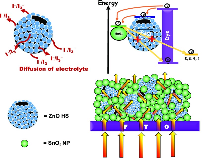
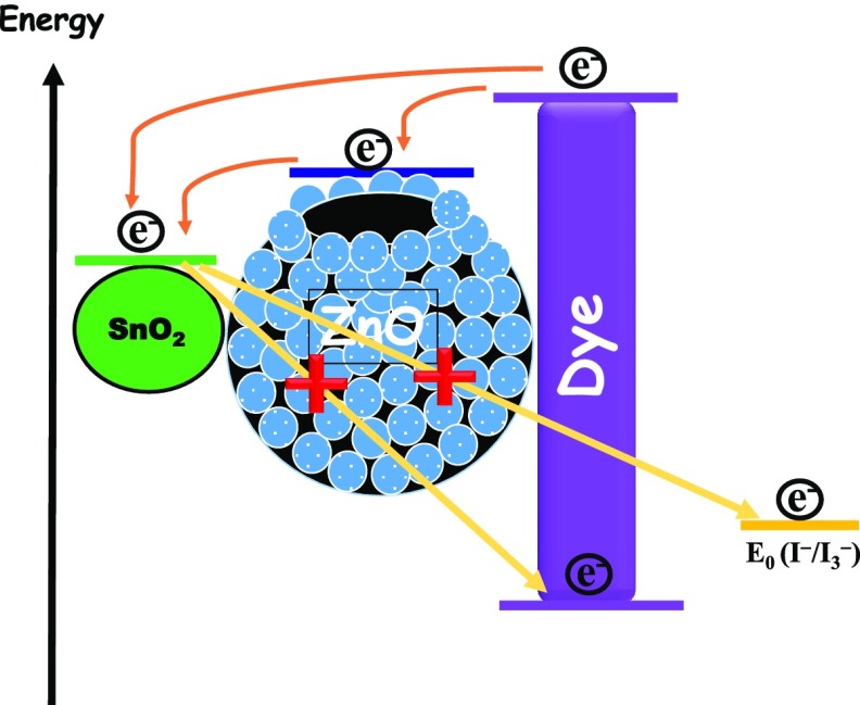
In the equivalent circuit, resistance Rs is the sheet resistance related to the resistance of the TCO, CE material; Rct1, the resistance of electrolyte, is the charge-transfer resistance of the counter electrode; CPE1 is the constant-phase element of the counter electrode; Rct2 is the charge-transfer resistance of the working electrode; and CPE2 is the constant-phase element of the working electrode. In the typical Nyquist plot, the semicircle in the mid-frequency region reveals the charge recombination resistance, which is attributed to the charge-transfer resistance (Rct2) at the metal oxide/sensitizer/electrolyte interface. As can be seen from Table 2, the charge recombination resistance Rct2 in the case of the SnO2 nanoparticle device is quite low, ∼39.5 Ω only, which is due to the higher recombination of the photogenerated electron at the SnO2/dye/electrolyte interface corroborating the current–voltage analysis. However, in the case of the composite photoanode, the value of Rct2 is much higher than that of the pristine SnO2 nanoparticle and further increases, i.e., from ∼121.2 Ω in the case of SZ10 to ∼146.3 Ω in SZ20 and is the highest in SZ30, ∼183.5 Ω, with an increase in the meso-ZnO HS content.59 This observation can be ascribed to inhibited recombination of photogenerated electrons with the introduction of ZnO hollow spheres having a higher conduction band level, as depicted in Scheme 3. Moreover, as can be seen from Table S4, there is a slight change in the Rct1 values of the as-fabricated devices, which may be due to the fact that Pt–FTO is used in all of the device combinations. However, a lower value of Rct1 among all of the devices in the case of the SZ20 corroborates a better catalytic activity as well as charge transfer dynamics of the counter electrode for this device.74,75 Moreover, mesoporous ZnO hollow spheres also facilitate the penetration of electrolyte to regenerate the oxidized dye.
Scheme 3. Schematic Representation of the Inhibited Electron Interception in the Case of the SnO2 NP_ZnO HS Composite Photoanode at the Semiconductor/Dye/Electrolyte Interface.
Corresponding Bode phase plots for the fabricated devices are represented in Figure 10. The two peaks at two different frequency regions endorse the two diode interfaces present in DSSCs. The characteristic phase angle peaks at the mid-frequency region are located at ∼40.3, ∼31.4, ∼14.6, and ∼12.4 Hz for pristine SnO2 nanoparticle, SZ10, SZ20, and SZ30 devices, respectively. From the Bode phase plot, the values of τe (photoinduced electron lifetime) are evaluated using the following relation, τe = 1/(2πfp), where fp is the observed maximum peak frequency in the mid-frequency region.25 It has been found that the τe values for different photoanodes are 3.9, 5.1, 10.9, and 12.6 ms for SnO2 nanoparticle, SZ10, SZ20, and SZ30 devices. The gradual increase in the photoinduced electron lifetime for the composite-based devices as compared to that for pristine SnO2 photoanode-based device with an increase in the meso-ZnO HS content also validates the interference created by addition of meso-ZnO HS, acting as a partial barrier for photoinduced electrons to undergo recombination at the semiconductor/dye/electrolyte interface. Moreover, a type II band alignment formed between well-matched band positions of SnO2 and ZnO heterostructures results in a charge carrier separation (electrons on SnO2 and holes on ZnO), which leads to reduced recombination and thus increases charge carrier lifetimes, as shown in Scheme 3.76
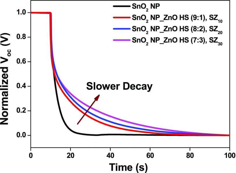
The electron recombination kinetics was further investigated by carrying out the transient open-circuit voltage decay measurement. Once the light is turned off under the open-circuit condition, the decrease in electron density in the CB and thus decay of the Voc is solely due to electron recombination.77 The Voc decay rate is directly determined by the recombination rate.
It is evident from the Voc decay that, as shown in Figure 11, the SnO2 nanoparticle-based photoanode shows a faster decay as compared with other composite photoanodes, corroborating the faster recombination kinetics in the device. The Voc decay becomes significantly slow as we move from SZ10 to SZ30, inferring a better charge transport and impeded recombination of photogenerated electrons on meso-ZnO HS loading. Although the charge transport properties of device with photoanode SZ30 is better than SZ20, till it furnishes lower efficiency that is mainly due to the less dye adsorption as well hindrance in light penetration resulting in a lower photogenerated electron thus decreases photogenerated current whereas the better performance of SZ20 device can be accredited to optimal concentration of meso-ZnO HS loading with combined effect of efficient light harvesting through optical absorption and confinement as well as enhanced charge transport properties at the interface.
Figure 11.
Normalized Voc decay curves for the fabricated devices based on the SnO2 nanoparticle film (black line), SnO2 NP_ZnO HS (9:1), SZ10 (red line); SnO2 NP_ZnO HS (8:2), SZ20 (blue line); and SnO2 NP_ZnO HS (7:3), SZ30 (magenta line).
4. Conclusions
In brief, a practical approach for superior light harnessing and impeded reverse tunneling of photogenerated electrons in a SnO2 NP-based device was demonstrated by introducing a cost-effective, easily synthesizable nano-amassed meso-ZnO HS. Micron-sized meso-ZnO HS can effectively scatter the incident light as well as traps the light inside the cavity by multiple reflections, thus increasing the probability of harnessing the incident light within the photoanode and thus enhancing the device efficacy. On the other hand, meso-ZnO HS can act as a thermodynamic energy barrier for back-recombination of photoinduced electrons at the working electrode/sensitizer/electrolyte interface owing to its higher CB position and also facilitates the diffusion of electrolyte through pores for regenerating the oxidized dye molecule. We have carried out systematic photovoltaic studies by varying the amount of meso-ZnO HS added in different ratios to SnO2, viz., SnO2 NP_ZnO HS (9:1), i.e., SZ10; SnO2 NP_ZnO HS (8:2), i.e., SZ20; SnO2 NP_ZnO HS (7:3), i.e., SZ30; and device SZ20 showed a nearly ∼4-fold increase in device efficacy as compared with the reference SnO2 NP-based device. The enhanced photovoltaic performance in the case of the composite devices can be accredited to efficient light harnessing and better interfacial charge transport properties on addition of nano-amassed meso-ZnO HS.
Acknowledgments
The work is financially supported by the Department of Science and Technology, India, through project no. DST/EMR/2016/005123. Infrastructural and instrumentation help from CIF, IIT Guwahati and IIT Guwahati is highly acknowledged.
Supporting Information Available
The Supporting Information is available free of charge on the ACS Publications website at DOI: 10.1021/acsomega.8b02520.
FESEM images of the SnO2 nanoparticle photoanode, cross-sectional FESEM images of the champion photoanode, top-view FESEM images of the champion photoanode, high-magnification TEM images of meso-ZnO hollow spheres, BET surface area analysis for SnO2 nanoparticles, photovoltaic performance of ZnO HS-based DSSCs, dye desorption analysis of the photoanodes, EDS mapping of the best-performing photoanode, comparative study of various SnO2_ZnO-based devices, stability tests for SZ20 and SnO2 nanoparticle-based solar cells, and EIS fitting data for devices (PDF)
The authors declare no competing financial interest.
Supplementary Material
References
- Horvath A. Construction materials and the environment. Annu. Rev. Environ. Resour. 2004, 29, 181–204. 10.1146/annurev.energy.29.062403.102215. [DOI] [Google Scholar]
- Schiermeier Q.; Tollefson J.; Scully T.; Witze A.; Morton O. Electricity without carbon. Nature 2008, 454, 816–823. 10.1038/454816a. [DOI] [PubMed] [Google Scholar]
- Grätzel M. Photoelectrochemical cells. Nature 2001, 414, 338–344. 10.1038/35104607. [DOI] [PubMed] [Google Scholar]
- O’Regan B.; Grätzel M. A Low-Cost, High-Efficiency Solar-Cell Based on Dye-Sensitized Colloidal TiO2 Films. Nature 1991, 353, 737–740. 10.1038/353737a0. [DOI] [Google Scholar]
- Mathew S.; Yella A.; Gao P.; Humphry-Baker R.; Curchod B. F. E.; Ashari-Astani N.; Tavernelli I.; Rothlisberger U.; Nazeeruddin M. K.; Gratzel M. Dye-sensitized solar cells with 13% efficiency achieved through the molecular engineering of porphyrin sensitizers. Nat. Chem. 2014, 6, 242–247. 10.1038/nchem.1861. [DOI] [PubMed] [Google Scholar]
- Zukalová M.; Zukal A.; Kavan L.; Nazeeruddin M. K.; Liska P.; Gratzel M. Organized mesoporous TiO2 films exhibiting greatly enhanced performance in dye-sensitized solar cells. Nano Lett. 2005, 5, 1789–1792. 10.1021/nl051401l. [DOI] [PubMed] [Google Scholar]
- Rensmo H.; Keis K.; Lindstrom H.; Sodergren S.; Solbrand A.; Hagfeldt A.; Lindquist S. E.; Wang L. N.; Muhammed M. High light-to-energy conversion efficiencies for solar cells based on nanostructured ZnO electrodes. J. Phys. Chem. B 1997, 101, 2598–2601. 10.1021/jp962918b. [DOI] [Google Scholar]
- Snaith H. J.; Ducati C. SnO2-Based Dye-Sensitized Hybrid Solar Cells Exhibiting Near Unity Absorbed Photon-to-Electron Conversion Efficiency. Nano Lett. 2010, 10, 1259–1265. 10.1021/nl903809r. [DOI] [PubMed] [Google Scholar]
- Kamat P. V.; Bedja I.; Hotchandani S.; Patterson L. K. Photosensitization of nanocrystalline semiconductor films. Modulation of electron transfer between excited ruthenium complex and SnO2 nanocrystallites with an externally applied bias. J. Phys. Chem. 1996, 100, 4900–4908. 10.1021/jp951269l. [DOI] [Google Scholar]
- Ferrere S.; Zaban A.; Gregg B. A. Dye sensitization of nanocrystalline tin oxide by perylene derivatives. J. Phys. Chem. B 1997, 101, 4490–4493. 10.1021/jp970683d. [DOI] [Google Scholar]
- Zheng H.; Tachibana Y.; Kalantar-zadeh K. Dye-Sensitized Solar Cells Based on WO3. Langmuir 2010, 26, 19148–19152. 10.1021/la103692y. [DOI] [PubMed] [Google Scholar]
- Chen S. G.; Chappel S.; Diamant Y.; Zaban A. Preparation of Nb2O5 coated TiO2 nanoporous electrodes and their application in dye-sensitized solar cells. Chem. Mater. 2001, 13, 4629–4634. 10.1021/cm010343b. [DOI] [Google Scholar]
- Burnside S.; Moser J. E.; Brooks K.; Gratzel M.; Cahen D. Nanocrystalline mesoporous strontium titanate as photoelectrode material for photosensitized solar devices: Increasing photovoltage through flatband potential engineering. J. Phys. Chem. B 1999, 103, 9328–9332. 10.1021/jp9913867. [DOI] [Google Scholar]
- Fonstad C. G.; Rediker R. H. Electrical Properties of High-Quality Stannic Oxide Crystals. J. Appl. Phys. 1971, 42, 2911–2918. 10.1063/1.1660648. [DOI] [Google Scholar]
- Qian J. F.; Liu P.; Xiao Y.; Jiang Y.; Cao Y. L.; Ai X. P.; Yang H. X. TiO2-Coated Multilayered SnO2 Hollow Microspheres for Dye-Sensitized Solar Cells. Adv. Mater. 2009, 21, 3663–3667. 10.1002/adma.200900525. [DOI] [Google Scholar]
- Arnold M. S.; Avouris P.; Pan Z. W.; Wang Z. L. Field-effect transistors based on single semiconducting oxide nanobelts. J. Phys. Chem. B 2003, 107, 659–663. 10.1021/jp0271054. [DOI] [Google Scholar]
- Senevirathna M. K. I.; Pitigala P. K. D. D. P.; Premalal E. V. A.; Tennakone K.; Kumara G. R. A.; Konno A. Stability of the SnO2/MgO dye-sensitized photo electrochemical solar cell. Sol. Energy Mater. Sol. Cells 2007, 91, 544–547. 10.1016/j.solmat.2006.11.008. [DOI] [Google Scholar]
- Teh J. J.; Guai G. H.; Wang X. W.; Leong K. C.; Li C. M.; Chen P. Nanoporous tin oxide photoelectrode prepared by electrochemical anodization in aqueous ammonia to improve performance of dye-sensitized solar cell. J. Renewable Sustainable Energy 2013, 5, 023120 10.1063/1.4798316. [DOI] [Google Scholar]
- Green A. N. M.; Palomares E.; Haque S. A.; Kroon J. M.; Durrant J. R. Charge transport versus recombination in dye-sensitized solar cells employing nanocrystalline TiO2 and SnO2 films. J. Phys. Chem. B 2005, 109, 12525–12533. 10.1021/jp050145y. [DOI] [PubMed] [Google Scholar]
- Parks G. A. Isoelectric Points of Solid Oxides Solid Hydroxides and Aqueous Hydroxo Complex Systems. Chem. Rev. 1965, 65, 177–198. 10.1021/cr60234a002. [DOI] [Google Scholar]
- Dou X.; Mathews N.; Wang Q.; Pramana S. S.; Lam Y. M.; Mhaisalkar S. Novel Zn-Sn-O nanocactus with excellent transport properties as photoanode material for high performance dye-sensitized solar cells. Nanoscale 2011, 3, 4640–4646. 10.1039/c1nr11083g. [DOI] [PubMed] [Google Scholar]
- Dou X. C.; Sabba D.; Mathews N.; Wong L. H.; Lam Y. M.; Mhaisalkar S. Hydrothermal Synthesis of High Electron Mobility Zn-doped SnO2 Nanoflowers as Photoanode Material for Efficient Dye-Sensitized Solar Cells. Chem. Mater. 2011, 23, 3938–3945. 10.1021/cm201366z. [DOI] [Google Scholar]
- Gubbala S.; Russell H. B.; Shah H.; Deb B.; Jasinski J.; Rypkema H.; Sunkara M. K. Surface properties of SnO2 nanowires for enhanced performance with dye-sensitized solar cells. Energy Environ. Sci. 2009, 2, 1302–1309. 10.1039/b910174h. [DOI] [Google Scholar]
- Gong J. W.; Qiao H.; Sigdel S.; Elbohy H.; Adhikari N.; Zhou Z. P.; Sumathy K.; Wei Q. F.; Qiao Q. Q. Characteristics of SnO2 nanofiber/TiO2 nanoparticle composite for dye-sensitized solar cells. AIP Adv. 2015, 5, 067134 10.1063/1.4922626. [DOI] [Google Scholar]
- Qureshi M.; Chetia T. R.; Ansari M. S.; Soni S. S. Enhanced photovoltaic performance of mesoporous SnO2 based solar cells utilizing 2D MgO nanosheets sensitized by a metal-free carbazole derivative. J. Mater. Chem. A 2015, 3, 4291–4300. 10.1039/C4TA05877A. [DOI] [Google Scholar]
- Ito S.; Makari Y.; Kitamura T.; Wada Y.; Yanagida S. Fabrication and characterization of mesoporous SnO2/ZnO-composite electrodes for efficient dye solar cells. J. Mater. Chem. 2004, 14, 385–390. 10.1039/b311090g. [DOI] [Google Scholar]
- Chen W.; Qiu Y. C.; Zhong Y. C.; Wong K. S.; Yang S. H. High-Efficiency Dye-Sensitized Solar Cells Based on the Composite Photoanocles of SnO2 Nanoparticles/ZnO Nanotetrapods. J. Phys. Chem. A 2010, 114, 3127–3138. 10.1021/jp908747z. [DOI] [PubMed] [Google Scholar]
- Milan R.; Selopal G. S.; Epifani M.; Natile M. M.; Sberveglieri G.; Vomiero A.; Concina I. ZnO@SnO2 engineered composite photoanodes for dye-sensitized solar cells. Sci. Rep. 2015, 5, 14523 10.1038/srep14523. [DOI] [PMC free article] [PubMed] [Google Scholar]
- Kay A.; Gratzel M. Dye-sensitized core-shell nanocrystals: Improved efficiency of mesoporous tin oxide electrodes coated with a thin layer of an insulating oxide. Chem. Mater. 2002, 14, 2930–2935. 10.1021/cm0115968. [DOI] [Google Scholar]
- Tributsch H. Dye sensitization solar cells: a critical assessment of the learning curve. Coord. Chem. Rev. 2004, 248, 1511–1530. 10.1016/j.ccr.2004.05.030. [DOI] [Google Scholar]
- Wu Q. Z.; Chen X.; Zhang P.; Han Y. C.; Chen X. M.; Yan Y. H.; Li S. P. Amino acid-assisted synthesis of ZnO hierarchical architectures and their novel photocatalytic activities. Cryst. Growth Des. 2008, 8, 3010–3018. 10.1021/cg800126r. [DOI] [Google Scholar]
- Thavasi V.; Renugopalakrishnan V.; Jose R.; Ramakrishna S. Controlled electron injection and transport at materials interfaces in dye-sensitized solar cells. Mater. Sci. Eng., R 2009, 63, 81–99. 10.1016/j.mser.2008.09.001. [DOI] [Google Scholar]
- Zhang T.; Dong W. J.; Keeter-Brewer M.; Konar S.; Njabon R. N.; Tian Z. R. Site-specific nucleation and growth kinetics in hierarchical nanosyntheses of branched ZnO crystallites. J. Am. Chem. Soc. 2006, 128, 10960–10968. 10.1021/ja0631596. [DOI] [PubMed] [Google Scholar]
- Lee Y. J.; Ruby D. S.; Peters D. W.; McKenzie B. B.; Hsu J. W. P. ZnO nanostructures as efficient antireflection layers in solar cells. Nano Lett. 2008, 8, 1501–1505. 10.1021/nl080659j. [DOI] [PubMed] [Google Scholar]
- Zhang Q. F.; Dandeneau C. S.; Zhou X. Y.; Cao G. Z. ZnO Nanostructures for Dye-Sensitized Solar Cells. Adv. Mater. 2009, 21, 4087–4108. 10.1002/adma.200803827. [DOI] [Google Scholar]
- Barpuzary D.; Banik A.; Panda A. N.; Qureshi M. Mimicking the Heteroleptic Dyes for an Efficient 1D-ZnO Based Dye-Sensitized Solar Cell Using the Homoleptic Ruthenium(II) Dipyridophenazine Complex as a Photosensitizer. J. Phys. Chem. C 2015, 119, 3892–3902. 10.1021/jp510422d. [DOI] [Google Scholar]
- Grätzel M. Conversion of sunlight to electric power by nanocrystalline dye-sensitized solar cells. J. Photochem. Photobiol., A 2004, 168, 235. 10.1016/j.jphotochem.2004.08.014. [DOI] [Google Scholar]
- Park Y. C.; Chang Y. J.; Kum B. G.; Kong E. H.; Son J. Y.; Kwon Y. S.; Park T.; Jang H. M. Size-tunable mesoporous spherical TiO2 as a scattering overlayer in high-performance dye-sensitized solar cells. J. Mater. Chem. 2011, 21, 9582–9586. 10.1039/c1jm11043h. [DOI] [Google Scholar]
- Grätzel M. Solar energy conversion by dye-sensitized photovoltaic cells. Inorg. Chem. 2005, 44, 6841–6851. 10.1021/ic0508371. [DOI] [PubMed] [Google Scholar]
- Ferber J.; Stangl R.; Luther J. An electrical model of the dye-sensitized solar cell. Sol. Energy Mater. Sol. Cells 1998, 53, 29–54. 10.1016/S0927-0248(98)00005-1. [DOI] [Google Scholar]
- Yu I. G.; Kim Y. J.; Kim H. J.; Lee C.; Lee W. I. Size-dependent light-scattering effects of nanoporous TiO2 spheres in dye-sensitized solar cells. J. Mater. Chem. 2011, 21, 532–538. 10.1039/C0JM02606A. [DOI] [Google Scholar]
- Huang F. Z.; Chen D. H.; Zhang X. L.; Caruso R. A.; Cheng Y. B. Dual-Function Scattering Layer of Submicrometer-Sized Mesoporous TiO2 Beads for High-Efficiency Dye-Sensitized Solar Cells. Adv. Funct. Mater. 2010, 20, 1301–1305. 10.1002/adfm.200902218. [DOI] [Google Scholar]
- Hore S.; Vetter C.; Kern R.; Smit H.; Hinsch A. Influence of scattering layers on efficiency of dye-sensitized solar cells. Sol. Energy Mater. Sol. Cells 2006, 90, 1176–1188. 10.1016/j.solmat.2005.07.002. [DOI] [Google Scholar]
- Banik A.; Ansari M. S.; Sahu T. K.; Qureshi M. Understanding the role of silica nanospheres with their light scattering and energy barrier properties in enhancing the photovoltaic performance of ZnO based solar cells. Phys. Chem. Chem. Phys. 2016, 18, 27818–27828. 10.1039/C6CP05544C. [DOI] [PubMed] [Google Scholar]
- Kim Y. J.; Lee M. H.; Kim H. J.; Lim G.; Choi Y. S.; Park N. G.; Kim K.; Lee W. I. Formation of Highly Efficient Dye-Sensitized Solar Cells by Hierarchical Pore Generation with Nanoporous TiO2 Spheres. Adv. Mater. 2009, 21, 3668–3673. 10.1002/adma.200900294. [DOI] [Google Scholar]
- Zhao P.; Wang L.; Yu Z.; Liu F.; Sun P.; Gao Y.; Lu G. Bilayered photoanode consisting of zinc oxide hollow spheres and urchin-like titanium dioxide microspheres enables fast electron transport and efficient light-harvesting for improved performance dye-sensitized solar cells. RSC Adv. 2016, 6, 17280–17287. 10.1039/C5RA25225C. [DOI] [Google Scholar]
- Zhang Q.; Chou T. R.; Russo B.; Jenekhe S. A.; Cao G. Z. Aggregation of ZnO nanocrystallites for high conversion efficiency in dye-sensitized solar cells. Angew. Chem., Int. Ed. 2008, 47, 2402–2406. 10.1002/anie.200704919. [DOI] [PubMed] [Google Scholar]
- Sauvage F.; Chen D. H.; Comte P.; Huang F. Z.; Heiniger L. P.; Cheng Y. B.; Caruso R. A.; Graetzel M. Dye-Sensitized Solar Cells Employing a Single Film of Mesoporous TiO2 Beads Achieve Power Conversion Efficiencies Over 10%. ACS Nano 2010, 4, 4420–4425. 10.1021/nn1010396. [DOI] [PubMed] [Google Scholar]
- Pham T. T. T.; Bessho T.; Mathews N.; Zakeeruddin S. M.; Lam Y. M.; Mhaisalkar S.; Gratzel M. Light scattering enhancement from sub-micrometer cavities in the photoanode for dye-sensitized solar cells. J. Mater. Chem. 2012, 22, 16201–16204. 10.1039/c2jm32401f. [DOI] [Google Scholar]
- Phama T. T. T.; Mathews N.; Lam Y. M.; Mhaisalkar S. Influence of size and shape of sub-micrometer light scattering centers in ZnO-assisted TiO2 photoanode for dye-sensitized solar cells. Phys. B 2018, 532, 225–229. 10.1016/j.physb.2017.03.016. [DOI] [Google Scholar]
- Deepak T. G.; Anjusree G. S.; Thomas S.; Arun T. A.; Nair S. V.; Nair A. S. A review on materials for light scattering in dye-sensitized solar cells. RSC Adv. 2014, 4, 17615–17638. 10.1039/C4RA01308E. [DOI] [Google Scholar]
- Wang H.; Miyauchi M.; Ishikawa Y.; Pyatenko A.; Koshizaki N.; Li Y.; Li L.; Li X. Y.; Bando Y.; Golberg D. Single-Crystalline Rutile TiO2 Hollow Spheres: Room-Temperature Synthesis, Tailored Visible-Light-Extinction, and Effective Scattering Layer for Quantum Dot-Sensitized Solar Cells. J. Am. Chem. Soc. 2011, 133, 19102–19109. 10.1021/ja2049463. [DOI] [PubMed] [Google Scholar]
- He C. X.; Lei B. X.; Wang Y. F.; Su C. Y.; Fang Y. P.; Kuang D. B. Sonochemical Preparation of Hierarchical ZnO Hollow Spheres for Efficient Dye-Sensitized Solar Cells. Chem. - Eur. J. 2010, 16, 8757–8761. 10.1002/chem.201000264. [DOI] [PubMed] [Google Scholar]
- Zhang Y. W.; Zhang J.; Wang P. Q.; Yang G. T.; Sun Q. A.; Zheng J.; Zhu Y. J. Anatase TiO2 hollow spheres embedded TiO2 nanocrystalline photoanode for dye-sensitized solar cells. Mater. Chem. Phys. 2010, 123, 595–600. 10.1016/j.matchemphys.2010.05.020. [DOI] [Google Scholar]
- Cui C.; Qiu Y. W.; Zhao J. H.; Lu B. Q.; Hu H. H.; Yang Y. N.; Ma N.; Xu S.; Xu L. B.; Li X. Y. A comparative study on the quantum-dot-sensitized, dye-sensitized and co-sensitized solar cells based on hollow spheres embedded porous TiO2 photoanodes. Electrochim. Acta 2015, 173, 551–558. 10.1016/j.electacta.2015.05.100. [DOI] [Google Scholar]
- Pang H.; Yang H. B.; Guo C. X.; Lu J. L.; Li C. M. Nanoparticle self-assembled hollow TiO2 spheres with well matching visible light scattering for high performance dye-sensitized solar cells. Chem. Commun. 2012, 48, 8832–8834. 10.1039/c2cc34355j. [DOI] [PubMed] [Google Scholar]
- Li K. N.; Wang Y. F.; Xu Y. F.; Chen H. Y.; Su C. Y.; Kuang D. B. Macroporous SnO2 Synthesized via a Template-Assisted Reflux Process for Efficient Dye-Sensitized Solar Cells. ACS Appl. Mater. Interfaces 2013, 5, 5105–5111. 10.1021/am4009727. [DOI] [PubMed] [Google Scholar]
- Rao J.; Yu A.; Shao C. L.; Zhou X. F. Construction of Hollow and Mesoporous ZnO Microsphere: A Facile Synthesis and Sensing Property. ACS Appl. Mater. Interfaces 2012, 4, 5346–5352. 10.1021/am3012966. [DOI] [PubMed] [Google Scholar]
- Banik A.; Ansari M. S.; Alam S.; Qureshi M. Thermodynamic Barrier and Light Scattering Effects of Nanocube Assembled SrTiO3 in Enhancing the Photovoltaic Properties of Zinc Oxide Based Dye Sensitized Solar Cells. J. Phys. Chem. C 2018, 122, 16550–16560. 10.1021/acs.jpcc.8b03623. [DOI] [Google Scholar]
- Huang X. K.; Hu Z. Y.; Xu J.; Wang P.; Wang L. M.; Zhang J.; Zhu Y. J. Low-temperature processed SnO2 compact layer by incorporating TiO2 layer toward efficient planar heterojunction perovskite solar cells. Sol. Energy Mater. Sol. Cells 2017, 164, 87–92. 10.1016/j.solmat.2017.02.010. [DOI] [Google Scholar]
- Barpuzary D.; Banik A.; Gogoi G.; Qureshi M. Noble metal-free counter electrodes utilizing Cu2ZnSnS4 loaded with MoS2 for efficient solar cells based on ZnO nanowires co-sensitized with CuInS2-CdSe quantum dots. J. Mater. Chem. A 2015, 3, 14378–14388. 10.1039/C5TA03396A. [DOI] [Google Scholar]
- Zhao Q.; Ju D. X.; Deng X. L.; Huang J. Z.; Cao B. Q.; Xu X. J. Morphology-modulation of SnO2 Hierarchical Architectures by Zn Doping for Glycol Gas Sensing and Photocatalytic Applications. Sci. Rep. 2015, 5, 7874 10.1038/srep07874. [DOI] [PMC free article] [PubMed] [Google Scholar]
- Rajalakshmi M.; Arora A. K.; Bendre B. S.; Mahamuni S. Optical phonon confinement in zinc oxide nanoparticles. J. Appl. Phys. 2000, 87, 2445–2448. 10.1063/1.372199. [DOI] [Google Scholar]
- Pradhan A. K.; Zhang K.; Loutts G. B.; Roy U. N.; Cui Y.; Burger A. Structural and spectroscopic characteristics of ZnO and ZnO: Er3+ nanostructures. J. Phys.: Condens. Matter 2004, 16, 7123–7129. 10.1088/0953-8984/16/39/043. [DOI] [Google Scholar]
- Cui Y. M.; Liu L.; Li B.; Zhou X. F.; Xu N. P. Fabrication of Tunable Core-Shell Structured TiO2 Mesoporous Microspheres Using Linear Polymer Polyethylene Glycol as Templates. J. Phys. Chem. C 2010, 114, 2434–2439. 10.1021/jp908613u. [DOI] [Google Scholar]
- Sing K. S. W.; Everett D. H.; Haul R. A. W.; Moscou L.; Pierotti R. A.; Rouquerol J.; Siemieniewska T. Reporting Physisorption Data for Gas Solid Systems with Special Reference to the Determination of Surface-Area and Porosity. Pure Appl. Chem. 1985, 57, 603–619. 10.1351/pac198557040603. [DOI] [Google Scholar]
- Gong J. W.; Liang J.; Sumathy K. Review on dye-sensitized solar cells (DSSCs): Fundamental concepts and novel materials. Renewable Sustainable Energy Rev. 2012, 16, 5848–5860. 10.1016/j.rser.2012.04.044. [DOI] [Google Scholar]
- Niinobe D.; Makari Y.; Kitamura T.; Wada Y.; Yanagida S. Origin of enhancement in open-circuit voltage by adding ZnO to nanocrystalline SnO2 in dye-sensitized solar cells. J. Phys. Chem. B 2005, 109, 17892–17900. 10.1021/jp051753g. [DOI] [PubMed] [Google Scholar]
- Desai U. V.; Xu C. K.; Wu J. M.; Gao D. Hybrid TiO2-SnO2 Nanotube Arrays for Dye-Sensitized Solar Cells. J. Phys. Chem. C 2013, 117, 3232–3239. 10.1021/jp3096727. [DOI] [Google Scholar]
- Li C.; Yang L.; Xiao J. Y.; Wu Y. C.; Sondergaard M.; Luo Y. H.; Li D. M.; Meng Q. B.; Iversen B. B. ZnO nanoparticle based highly efficient CdS/CdSe quantum dot-sensitized solar cells. Phys. Chem. Chem. Phys. 2013, 15, 8710–8715. 10.1039/c3cp50365h. [DOI] [PubMed] [Google Scholar]
- Kim Y. J.; Lee M. H.; Kim H. J.; Lim G.; Choi Y. S.; Park N. G.; Kim K.; Lee W. I. Formation of Highly Efficient Dye-Sensitized Solar Cells by Hierarchical Pore Generation with Nanoporous TiO2 Spheres. Adv. Mater. 2009, 21, 3668–3673. 10.1002/adma.200900294. [DOI] [Google Scholar]
- Barpuzary D.; Qureshi M. Enhanced Photovoltaic Performance of Semiconductor-Sensitized ZnO-CdS Coupled with Graphene Oxide as a Novel Photoactive Material. ACS Appl. Mater. Interfaces 2013, 5, 11673–11682. 10.1021/am403268w. [DOI] [PubMed] [Google Scholar]
- Ansari M. S.; Banik A.; Qureshi M. Morphological tuning of photo-booster g-C3N4 with higher surface area and better charge transfers for enhanced power conversion efficiency of quantum dot sensitized solar cells. Carbon 2017, 121, 90–105. 10.1016/j.carbon.2017.05.075. [DOI] [Google Scholar]
- Qian X.; Li H. M.; Shao L.; Jiang X. C.; Hou L. X. Morphology-Tuned Synthesis of Nickel Cobalt Selenides as Highly Efficient Pt-Free Counter Electrode Catalysts for Dye-Sensitized Solar Cells. ACS Appl. Mater. Interfaces 2016, 8, 29486–29495. 10.1021/acsami.6b09966. [DOI] [PubMed] [Google Scholar]
- Li H. M.; Qian X.; Zhu C. L.; Jiang X. X.; Shao L.; Hou L. X. Template synthesis of CoSe2/Co3Se4 nanotubes: tuning of their crystal structures for photovoltaics and hydrogen evolution in alkaline medium. J. Mater. Chem. A 2017, 5, 4513–4526. 10.1039/C6TA10718D. [DOI] [Google Scholar]
- Uddin M. T.; Nicolas Y.; Olivier C.; Toupance T.; Servant L.; Muller M. M.; Kleebe H. J.; Ziegler J.; Jaegermann W. Nanostructured SnO2-ZnO Heterojunction Photocatalysts Showing Enhanced Photocatalytic Activity for the Degradation of Organic Dyes. Inorg. Chem. 2012, 51, 7764–7773. 10.1021/ic300794j. [DOI] [PubMed] [Google Scholar]
- Zaban A.; Greenshtein M.; Bisquert J. Determination of the electron lifetime in nanocrystalline dye solar cells by open-circuit voltage decay measurements. ChemPhysChem 2003, 4, 859–864. 10.1002/cphc.200200615. [DOI] [PubMed] [Google Scholar]
Associated Data
This section collects any data citations, data availability statements, or supplementary materials included in this article.


