

Abstract

Recent evidence for bimolecular nonradiative recombination in lead-halide perovskites poses the question for a mechanistic origin of such a recombination term. A possible mechanism is Auger recombination involving two free charge carriers and a trapped charge-carrier. To study the influence of trap-assisted Auger recombination on bimolecular recombination in lead-halide perovskites, we combine estimates of the transition rates with a detailed balance compatible approach of calculating the occupation statistics of defect levels using a similar approach as for the well-known Shockley–Read–Hall recombination statistics. We find that the kinetics resulting from trap-assisted Auger recombination encompasses three different regimes: low injection, high injection, and saturation. Although the saturation regime with a recombination rate proportional to the square of free carrier concentration might explain the nonradiative bimolecular recombination in general, we show that the necessary trap density is higher than reported. Thus, we conclude that Auger recombination via traps is most likely not the explanation for the observed nonradiative bimolecular recombination in CH3NH3PbI3 and related materials.
Introduction
One of the key prerequisites for optoelectronic materials are long nonradiative lifetimes1−7 for recombination via defects as compared to the recombination coefficients for direct radiative band-to-band transitions.8−13 Recombination via defects14,15 is usually assumed to be mediated by the emission of multiple phonons,16−21 whereas band-to-band recombination via multiphonon emission is thought to be extremely unlikely in inorganic semiconductors.22 Because the transition rates are strongly reduced for an increasing number of phonons17,22 involved in a single transition at low-to-moderate strength of electron–phonon coupling, direct band-to-band recombination is typically assumed to be entirely radiative in inorganic semiconductors. This is different in organic semiconductors due to the higher energy associated with molecular vibrations in organic molecules relative to the energy of phonons in inorganic semiconductors.23 Given that lead-halide perovskites due to the high atomic mass of Pb and I have particularly low phonon energies,24,25 it is initially rather surprising that there is evidence26,27 for recombination terms that are quadratic in charge-carrier density (like radiative recombination in high-level injection) and are nonradiative. In addition to multiphonon recombination, Auger recombination is the second archetypal nonradiative recombination mechanism.13,28−30 Auger recombination involving two free electrons and one hole or two free holes and one electron, respectively, should be cubic in charge-carrier density in the high-level injection and would therefore not be able to explain the observed features. However, Auger recombination involving trapped charge carriers could in principle explain the observed quadratic behavior.26
Thus far, trap-assisted Auger recombination has been mainly discussed for the case of highly doped semiconductors29−31 where this mechanism is most efficient because of the high density of free charge carriers. This implies that only the limiting linear case of low injection (with respect to the doping level) is usually considered. In addition, it has been discussed in the context of determining limiting efficiencies for Si solar cells, but recently also for perovskite solar cells.13,28,30,32 To study the potential effect of trap-assisted Auger recombination on bimolecular recombination in lead-halide perovskites close to the radiative limit, a model for the full recombination statistics is required. Therefore, we develop a detailed balance compatible rate equation model in analogy to the Shockley–Read–Hall (SRH) recombination statistics.14,15 Subsequently, we use known material properties of the lead-halide perovskites and previously derived equations33 for the transition rates to estimate the Auger coefficients for trap-assisted Auger recombination in perovskites. Finally, we derive the necessary trap density for trap-assisted Auger recombination to explain the observed nonradiative contribution to bimolecular recombination. The necessary defect density is at least on the order of 1017 cm–3 for midgap defects and increases for more shallow defects. This defect density is about 1 order of magnitude higher than the defect densities that have so far been observed in the experiment.34,35 Thus, we conclude that the trap-assisted Auger recombination is unlikely to be the reason for the observed nonradiative bimolecular recombination and probably does not pose a fundamental limitation to the efficiency of the lead-halide perovskites.
Results and Discussion
Recombination Statistics
The complete picture of the Auger processes involving traps as outlined in ref (33) is illustrated in Figure 1. In total, four processes can be summarized by four transition coefficients T1...T4:
-
(1)
two electrons e and an empty trap ht transform into an electron e* (at nonthermal energy) and a trapped electron et according to the reaction scheme: 2e + ht ↔ e* + et.
-
(2)
an electron, a hole h, and an empty trap transform into a hole h* (at nonthermal energy) and a trapped electron: e + h + ht ↔ h* + et.
-
(3)
an electron, a hole, and a trapped electron transform into an electron (at nonthermal energy) and an empty trap: e + h + et ↔ e* + ht.
-
(4)
two holes and a trapped electron transform into a hole (at nonthermal energy) and an empty trap: 2h + et ↔ h* + ht.
Figure 1.

Illustration of various interactions between free charge carriers and defect states resulting in electron capture (with coefficients T1, T2) and hole capture (T3, T4), respectively. Please note that the processes 2 and 3 consist of two possible interactions each. The energy levels of the valence and conduction bands are here denoted as EV and EC, respectively. Furthermore, Et marks the imperfection level (trap depth).
Thus, processes 1 and 2 result in electron capture and processes 3 and 4 in hole capture such that a net recombination of an electron–hole pair requires a combination of steps 1 or 2 with 3 or 4.
To fulfill the requirements of detailed balance, we also have to consider the back reactions, i.e., impact ionization of trapped electrons or holes via hot electrons or holes. The rates R1...4,b for the back reactions are determined by the Auger coefficients C1...4* such that we have, e.g., for back 1R1,b = C1n*N, where n* denotes the concentration of hot electrons and N the concentration of filled traps. If we assume that the thermalization of charge carriers is faster than the Auger processes or their inverses, the ratio between n* and the overall concentration n of electrons is constant and corresponds to the ratio n0*/n0 between both concentrations at thermal equilibrium. Thus, we define the coefficient C1 = C1n0*/n0 and, analogously, C2 = C2p0*/p0, C3 = C3n0*/n0, and C4 = C4p0*/p0 using p0, p0, p*, and p as the analogous variables for the holes. Then, the rates for the four transitions can be written as
| 1 |
| 2 |
| 3 |
and
| 4 |
Here, we use the abbreviations
| 5 |
and
| 6 |
where n0 and p0 are the equilibrium concentrations of the electrons and the holes. The concentrations n1 and p1 correspond to the values of n and p, when the Fermi level lies at the trap depth ET. We eliminate the parameters C1,...,C4 in eqs 1–4 by using the principle of detailed balance36 and expressing them as a product of T1,...,T4 multiplied with either n1 or p1 in analogy to the derivation of Shockley–Read–Hall statistics. By assuming steady-state conditions dN/dt = 0, we may eliminate the concentration N of filled traps by writing
| 7 |
We then obtain for the (normalized) density of occupied trap states
 |
8 |
The final recombination rate RTA is subsequently given by inserting eq 8 into RTA = R1 + R2 = R3 + R4 and is given by
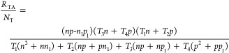 |
9 |
Simulation Results
Figure 2a illustrates eq 9 as a function of the excess charge-carrier concentration Δn = n – n0 using the parameters given in Table 1. The rate of Auger recombination involving interactions with defect states exhibits three regimes with different dependencies of RTA on the excess charge-carrier concentration Δn. We assume the semiconductor to be p-type (n0 ≪ p0) in this example (doping density NA = 3 × 1015 cm–3),37 thus, for Δn ≪ NA, we are in low-level injection conditions. In addition, we assume the defect to be close to the conduction band, i.e., n1 ≫ p ≫ p1. In this case, eq 9 simplifies to
| 10 |
i.e., the recombination rate scales linearly with Δn = n. This linear scaling is independent of the position of the trap and would also happen for a midgap trap, in which case, the rate would be
| 11 |
For higher excess charge densities, Δn > NA, we enter high-level injection conditions, where we may simplify eq 9 using the conditions n1 ≫ n = p = Δn ≫ p1 (for a trap close to the conduction band edge). Then, we obtain
| 12 |
i.e., a cubic relation between the rate and the excess carrier concentration. Only in the saturation regime, where n = p = Δn ≫ n1 ≫ p1, the recombination rate
| 13 |
starts to scale quadratically with Δn. Thus, the three regimes visible in Figure 2a differ from the situation encountered for Auger recombination of free charge carriers. Here, also three regimes are visible, but the order for the Auger recombination rate RA (for free carriers) is RA ∼ Δn (for low-level injection), RA ∼ Δn2 (for n ≈ p), and RA ∼ Δn3 for high-level injection. In contrast, the Auger recombination via traps features an intermediate cubic scaling law as long as the doping concentration is smaller than either n1 or p1. To estimate the magnitude of trap-assisted Auger recombination for the specific case of lead-halide perovskites, we use equations for the transition coefficients T1,...,T4 derived by Landsberg et al.,33 which are given by
| 14 |
where Table 2 provides the values for the abbreviations Ni, di, and bi for i = 1,...,4.
Figure 2.

(a, c) Recombination rate and (b, d) effective lifetime as a function of charge-carrier concentration. (a) The situation of a shallow trap (ET = 0.1 eV) with the solid gray line indicating the total trap-assisted Auger recombination and the dotted lines illustrate the approximations given by eqs 10, 12, and 13 valid in three different injection regimes. (c) The equivalent plot for the case of a midgap trap, which only shows a linear regime at low Δn and a quadratic regime at high Δn. (b) The effective lifetime τeff for Auger recombination via traps assuming a trap density NT = 1018 cm–3 and the radiative lifetime τrad = Δn/Rrad assuming Rrad = kradnp, with krad = 10–10 cm3/s. (d) The effective lifetime for a deep trap. For comparison, we also added the values for SRH recombination using capture coefficients determined as discussed in ref (22) and using different trap densities that are lower than the one for trap-assisted Auger recombination.
Table 1. Input Parameters Used for the Calculations Presented in Figures 2 and 3 if Not Otherwise Stateda.
| band gap | Eg | 1.6 eV |
| effective mass of electrons | me | 0.2m0 |
| effective mass of holes | mh | 0.2m0 |
| relative permittivity | εr | 33.524 |
Table 2. Definition of the Abbreviations Used To Determine the Trap-Assisted Auger Recombination Coefficients Ti Using Equation 15a.
| i | Ni | di1 | di2 | bi | ||||
|---|---|---|---|---|---|---|---|---|
| 1 | 13 | –260 | ||||||
| 2 | 0.5(33 – 15σL) | 0.5(33 – 15σL) | ||||||
| 3 | ||||||||
|
||||||||
| 4 | ||||||||

Here, Eg is the band gap, Et is the trap depth with respect to the conduction band, σ = mh/me is the ratio of the hole and electron effective mass, and σL = 1/σ. In this form, the notation is valid for free electrons in the conduction band interacting with defect states. For free holes in the valence band, Et, σ, and σL have to be adjusted accordingly.
Figure 2b shows the resulting effective lifetime τeff for the trap-assisted Auger recombination assuming a high trap density of 1018 cm–3. We define the effective lifetime for a given process as τeff = Δn/R, where R is the recombination rate for a certain recombination mechanism. The effective lifetime τTA for the trap-assisted Auger recombination is therefore defined as τTA = Δn/RTA, whereas the effective radiative lifetime is τrad = Δn/Rrad. Here, Rrad is the radiative recombination rate. We note that for low-excess charge-carrier concentrations Δn, both the trap-assisted Auger recombination and radiative recombination lead to a constant effective lifetime, consistent with the recombination rate increasing linearly with Δn in both cases. Once Δn exceeds the doping concentration assumed to be NA = 3 × 1015 cm–3, the Auger lifetime drops drastically until Δn ≈ n1, at which point the slope gets flatter again. This is the logical consequence of the three regimes for RTA seen in Figure 2a. We also note that even for such a high trap density of NT = 1018 cm–3, the radiative lifetime is lower for all values of Δn.
Figure 2c,d show the situation of a deep trap first for the recombination rate (c) and subsequently for the effective lifetime (d). For deep traps, n1 is very small (n1 ≪ NA), thus there exist only two regimes (low injection and high injection), but no saturation regime. In consequence, the effective lifetimes for radiative and trap-assisted Auger recombination have the same shape. For the assumed values of krad and NT, the values for τTA and τrad are quite similar. In Figure 2d, we also show for comparison the effective Shockley–Read–Hall lifetime via a deep trap. We do these calculations based on the theory of multiphonon recombination discussed in ref (22) and based on refs (17) and (18). Here, we observe that for trap densities already much lower than used for Auger recombination via traps, the SRH lifetime dominates over a wide range of Δn values.
Having established the general features of the recombination statistics of Auger recombination involving traps, we now want to investigate more closely under which circumstances the recombination rate is comparable to the radiative recombination rate. In particular, we are interested in the case described by eq 13, where the scaling is quadratic. In this scenario, we may define the total bimolecular recombination rate Rbm as
 |
15 |
i.e., the sum of radiative recombination (kradn2), minus the amount of light that is reabsorbed and contributes to the internal generation (prkradn2, with pr being the probability of reabsorption37,38) plus the trap-assisted Auger recombination. Figure 3a illustrates the effective Auger coefficient CT ≡ kTA/NT as a function of trap depth ET. As it is the case for Shockley–Read–Hall statistics, also the Auger recombination rate via defects shows its maximum for midgap traps, when detrapping of captured charge carries is least likely. The vertical dashed lines represent intrinsic defect levels according to the density functional theory calculations as reported in ref (39). In the next step, we evaluate the defect density NT, which has to be present in the samples to cause a certain nonradiative bimolecular recombination coefficient knon. Table 3 shows the experimental data from various groups on the total, radiative, and nonradiative bimolecular recombination coefficient. The values for the nonradiative recombination coefficient vary quite strongly. Therefore, we vary knon in the range between 10–12 and 10–10 cm3/s and show the necessary trap density as a function of trap position in Figure 3b. In comparison, we show the necessary trap depth to achieve a monomolecular Shockley–Read–Hall type lifetime τSRH = 1 μs assuming the multiphonon transitions as discussed in ref (22). We judge from Figure 3b that deep trap densities >1017 cm–3 are needed for midgap traps and higher for shallower traps. Although such trap densities at midgap would lead to very short SRH lifetimes that are not consistent with experiment, such trap densities may explain the experimental data if the trap is not midgap but at a trap depth of around 0.5–0.6 eV away from either the conduction or valence band. To put these densities into context, Table 4 compares the trap densities that have been measured on CH3NH3PbI3 in the literature. Table 4 suggests that so far most experimentally observed trap densities are in the range of 1015–1016 cm–3, i.e., in a range that would not lead to substantial trap-assisted Auger recombination.
Figure 3.

(a) Coefficient CT of trap-assisted Auger recombination as a function of the trap depth ET with respect to the conduction band edge EC. Vertical dashed lines represent trap depths of various intrinsic defects according to ref (39). (b) Trap density NT as a function of trap depths ET that would be needed to cause a nonradiative bimolecular recombination coefficient of 10–11 and 10–10 cm3/s (light blue and dark blue curves, respectively). In addition, we added the trap density needed to achieve a 1 μs monomolecular lifetime as calculated in ref (22) based on the theory of multiphonon Shockley–Read–Hall recombination.
Table 3. Values for the Bimolecular Recombination Coefficients in Units of cm3/s of CH3NH3PbI3 from Literature.
Table 4. Trap Densities Reported for CH3NH3PbI3 Thin Films in the Literature.
| reference | method | trap density (cm–3) | trap depth ET (eV) |
|---|---|---|---|
| (34) | thermally stimulated current (TSC) | >1015 | ∼0.5 |
| (55) | noise spectroscopy | 4 × 10¹⁵ | ∼0.8 |
| (56) | deep level transient spectroscopy (DLTS) | ∼1015 | 0.62 |
| ∼1015 | 0.75 | ||
| (57) | steady state photocarrier grating | >1016 | recombination center |
| (58) | TSC | 9 × 10¹⁶ | 0.18 |
| 5 × 10¹⁶ | 0.49 | ||
| (59) | admittance spectroscopy | ∼1016 cm–3 | 0.16 |
| (60) | admittance spectroscopy | ∼1016 cm–3 a | 0.27 |
| ∼1017 cm–3 b | 0.28 | ||
| (35) | DLTS | 9 × 10¹³ to 5 × 1014 cm–3 | 0.78 |
Dimethylformamide as solvent with hydroiodic acid as additive.
Dimethyl sulfoxide as solvent.
Discussion and Outlook
Having established that Auger recombination via traps is not likely to explain the observed nonradiative contributions to bimolecular recombination, it is useful to discuss the implications of this result and consider alternative explanations for the observed trends. First, we want to state that most experimental approaches to study bimolecular recombination would not be sensitive to whether bimolecular recombination is radiative or nonradiative. In most cases, the transient decay is fitted with a model that accounts for bimolecular recombination. In the case of transient photoluminescence experiments, it is clear that some of this recombination has to be radiative to generate a signal, but the determination of how much of this bimolecular recombination is radiative would require additional information. This information can either be another experiment that determines the total recombination as done by Richter et al.26 or some experimental circumstances that would distinguish radiative from nonradiative such as the sensitivity of radiative recombination to parasitic absorption via the modulation of the photon recycling probability as done previously by us.27 Certainly, two sets of experimental evidence we are aware of are not very much and future will tell whether these results are reproduced by others or are a peculiar feature of the samples or the data analysis in these articles. However, assuming that the data are representative, we want to briefly explore what other explanations there might be.
In a simple zero-dimensional picture, the authors are not aware of any recombination mechanism that would be quadratic in charge-carrier density and still be nonradiative other than the one discussed here. Thus, it is logical to explore effects requiring more dimensions. There are essentially two options in our opinion: (i) diffusion of carriers at high-level injection inside the films leads to a decrease in signal that could be interpreted as a recombination but is not or (ii) lateral inhomogeneous lifetimes lead to a distribution of decay times that creates a decay that appears quadratic in the charge-carrier density but is not related to locally quadratic recombination mechanisms. Let us briefly look into the two options in more detail. After the excitation of a sample with a laser pulse, electrons and holes are created based on the generation profile of the sample. Disregarding interferences, it is clear that more electrons and holes would be created close to the front surface of the sample and less toward the back. As long as the electron and hole concentrations are roughly equal, the luminescence is higher than after equilibration of the charge-carrier distribution. This leads to a decay in the luminescence that requires no recombination to happen. Diffusion of charge carriers during a transient photoluminescence experiment has been taken into account in the classical theory articles on transient photoluminescence experiments,40,41 in first experiments on perovskite films with contact layers,42 and in the case of transient experiments on perovskite crystals.43,44 However, given the range of mobilities that is commonly reported,45,46 diffusion and equilibration of charge carriers in a film of few hundreds of nanometer thickness should happen in the sub-nanosecond range (e.g., ∼300 ps for a 300 nm film and a mobility of 20 cm2/(V s)). Thus, for this explanation to affect the experiments, there have to be at least some charge carriers with a substantially lower mobility to see an effect on the time scale where bimolecular recombination is typically observed.
The second option is laterally inhomogeneous lifetimes that have been reported and studied in a range of publications.47,48 If by averaging over a certain area, the macroscopic decay curve does not capture one lifetime but a broad distribution of lifetimes, the tail of this distribution toward shorter lifetimes could influence the shorter time scales of a transient photoluminescence experiment and thereby affect the way we interpret the data. Future work of modeling the photoluminescence in two or three dimensions will have to show whether this is a likely explanation for the observed data in refs (26, 27). Both of these alternative approaches to explain the experimental data would not be a unique feature of every MAPI sample, but instead could vary from sample to sample. They would therefore not contradict reports6,7 of extremely high photoluminescence quantum efficiencies that leave little room for additional nonradiative pathways.
Conclusions
In summary, we have developed a rate model for the full recombination statistic of electrons and holes via trap-assisted Auger recombination. The model covers the linear low injection case with a recombination rate RTA ∝ Δn proportional to the density of excess charge carriers Δn, as well as two nonlinear situations, namely, high-level injection with RTA ∝ Δn3 and the saturation situation with RTA ∝ Δn2. The latter case represents the bimolecular recombination that directly competes with radiative recombination. As an example, our calculations following the theory of ref (33) yield the actual rates for the case of CH3NH3PbI3. The coefficients for this specific case are however relatively small. Therefore, we conclude that this mechanism is not likely to be the origin of the experimentally measured nonradiative bimolecular recombination coefficients.
Acknowledgments
T.K. and U.R. acknowledge support from the DFG (Grant Nos. KI-1571/2-1 and RA 473/7-1) and from the Helmholtz Association via the PEROSEED project. T.K. thanks Igal Levine (Weizmann, Rehovot) for sharing most of the references for Table 4.
The authors declare no competing financial interest.
References
- Correa-Baena J. P.; Saliba M.; Buonassisi T.; Grätzel M.; Abate A.; Tress W.; Hagfeldt A. Promises and Challenges of Perovskite Solar Cells. Science 2017, 358, 739. 10.1126/science.aam6323. [DOI] [PubMed] [Google Scholar]
- Tress W. Perovskite Solar Cells on the Way to Their Radiative Efficiency Limit – Insights Into a Success Story of High Open-Circuit Voltage and Low Recombination. Adv. Energy Mater. 2017, 7, 1602358 10.1002/aenm.201602358. [DOI] [Google Scholar]
- Ahrenkiel R. K.Minority-Carrier Lifetime in III–V Semiconductors. In Minority Carriers in III–V Semiconductors: Physics and Applications; Elsevier: 1993; Vol. 39, pp 39–150. [Google Scholar]
- Sinton R. A.; Cuevas A. Contactless Determination of Current-Voltage Characteristics and Minority-Carrier Lifetimes in Semiconductors From Quasi-Steady-State Photoconductance Data. Appl. Phys. Lett. 1996, 69, 2510–2512. 10.1063/1.117723. [DOI] [Google Scholar]
- Credgington D.; Durrant J. R. Insights From Transient Optoelectronic Analyses on the Open-Circuit Voltage of Organic Solar Cells. J. Phys. Chem. Lett. 2012, 3, 1465–1478. 10.1021/jz300293q. [DOI] [PubMed] [Google Scholar]
- Abdi-Jalebi M.; Andaji-Garmaroudi Z.; Cacovich S.; Stavrakas C.; Philippe B.; Richter J. M.; Alsari M.; Booker E. P.; Hutter E. M.; Pearson A. J.; et al. Maximizing and Stabilizing Luminescence From Halide Perovskites With Potassium Passivation. Nature 2018, 555, 497. 10.1038/nature25989. [DOI] [PubMed] [Google Scholar]
- Braly I. L.; deQuilettes D. W.; Pazos-Outon L. M.; Burke S.; Ziffer M. E.; Ginger D. S.; Hillhouse H. W. Hybrid Perovskite Films Approaching the Radiative Limit With Over 90% Photoluminescence Quantum Efficiency. Nat. Photonics 2018, 12, 355–361. 10.1038/s41566-018-0154-z. [DOI] [Google Scholar]
- Ross R. T. Some Thermodynamics of Photochemical Systems. J. Chem. Phys. 1967, 46, 4590–4593. 10.1063/1.1840606. [DOI] [Google Scholar]
- Smestad G.; Ries H. Luminescence and Current Voltage Characteristics of Solar-Cells and Optoelectronic Devices. Sol. Energy Mater. Sol. Cells 1992, 25, 51–71. 10.1016/0927-0248(92)90016-I. [DOI] [Google Scholar]
- Rau U. Reciprocity Relation Between Photovoltaic Quantum Efficiency and Electroluminescent Emission of Solar Cells. Phys. Rev. B 2007, 76, 085303 10.1103/PhysRevB.76.085303. [DOI] [Google Scholar]
- Steiner M. A.; Geisz J. F.; Garcia I.; Friedman D. J.; Duda A.; Olavarria W. J.; Young M.; Kuciauskas D.; Kurtz S. R. Effects of Internal Luminescence and Internal Optics on Voc and Jsc of III-V Solar Cells. IEEE J. Photovoltaics 2013, 3, 1437–1442. 10.1109/JPHOTOV.2013.2278666. [DOI] [Google Scholar]
- Miller O. D.; Yablonovitch E.; Kurtz S. R. Strong Internal and External Luminescence As Solar Cells Approach the Shockley-Queisser Limit. IEEE J. Photovoltaics 2012, 2, 303–311. 10.1109/JPHOTOV.2012.2198434. [DOI] [Google Scholar]
- Tiedje T.; Yablonovitch E.; Cody G. D.; Brooks B. G. Limiting Efficiency of Silicon Solar-Cells. IEEE Trans. Electron Devices 1984, 31, 711–716. 10.1109/T-ED.1984.21594. [DOI] [Google Scholar]
- Shockley W.; Read W. T. Statistics of the Recombination of Holes and Electrons. Phys. Rev. 1952, 87, 835–842. 10.1103/PhysRev.87.835. [DOI] [Google Scholar]
- Hall R. N. Electron-Hole Recombination in Germanium. Phys. Rev. 1952, 87, 387. 10.1103/PhysRev.87.387. [DOI] [Google Scholar]
- Markvart T.Multiphonon recombination. In Recombination in Semiconductors; Landsberg P. T., Ed.; Cambridge University Press: Cambridge, 2003; p 470. [Google Scholar]
- Markvart T. Semiclassical Theory of Non-Radiative Transitions. J. Phys. C: Solid State Phys. 1981, 14, L895. 10.1088/0022-3719/14/29/006. [DOI] [Google Scholar]
- Ridley B. K. On the Multiphonon Capture Rate in Semiconductors. Solid-State Electron. 1978, 21, 1319–1323. 10.1016/0038-1101(78)90200-9. [DOI] [Google Scholar]
- Ridley B. K. Multiphonon, Non-Radiative Transition Rate for Electrons in Semiconductors and Insulators. J. Phys. C: Solid State Phys. 1978, 11, 2323. 10.1088/0022-3719/11/11/023. [DOI] [Google Scholar]
- Henry C. H.; Lang D. V. Nonradiative Capture and Recombination by Multiphonon Emission in GaAs and GaP. Phys. Rev. B 1977, 15, 989–1016. 10.1103/PhysRevB.15.989. [DOI] [Google Scholar]
- Kirchartz T.; Rau U. What Makes a Good Solar Cell?. Adv. Energy Mater. 2018, 1703385 10.1002/aenm.201703385. [DOI] [Google Scholar]
- Kirchartz T.; Markvart T.; Rau U.; Egger D. A. Impact of Small Phonon Energies on the Charge-Carrier Lifetimes in Metal-Halide Perovskites. J. Phys. Chem. Lett. 2018, 9, 939–946. 10.1021/acs.jpclett.7b03414. [DOI] [PubMed] [Google Scholar]
- Benduhn J.; Tvingstedt K.; Piersimoni F.; Ullbrich S.; Fan Y.; Tropiano M.; McGarry K. A.; Zeika O.; Riede M. K.; Douglas C. J.; et al. Intrinsic Non-Radiative Voltage Losses in Fullerene-Based Organic Solar Cells. Nat. Energy 2017, 2, 17053 10.1038/nenergy.2017.53. [DOI] [Google Scholar]
- Sendner M.; Nayak P. K.; Egger D. A.; Beck S.; Muller C.; Epding B.; Kowalsky W.; Kronik L.; Snaith H. J.; Pucci A.; et al. Optical Phonons in Methylammonium Lead Halide Perovskites and Implications for Charge Transport. Mater. Horiz. 2016, 3, 613–620. 10.1039/C6MH00275G. [DOI] [Google Scholar]
- Wright A. D.; Verdi C.; Milot R. L.; Eperon G. E.; Perez-Osorio M. A.; Snaith H. J.; Giustino F.; Johnston M. B.; Herz L. M. Electron–Phonon Coupling in Hybrid Lead Halide Perovskites. Nat. Commun. 2016, 7, 11755 10.1038/ncomms11755. [DOI] [PMC free article] [PubMed] [Google Scholar]
- Richter J. M.; Abdi-Jalebi M.; Sadhanala A.; Tabachnyk M.; Rivett J. P. H.; Pazos-Outon L. M.; Gödel K. C.; Price M.; Deschler F.; Friend R. H. Enhancing Photoluminescence Yields in Lead Halide Perovskites by Photon Recycling and Light Out-Coupling. Nat. Commun. 2016, 7, 13941 10.1038/ncomms13941. [DOI] [PMC free article] [PubMed] [Google Scholar]
- Staub F.; Kirchartz T.; Bittkau K.; Rau U. Manipulating the Net Radiative Recombination Rate in Lead Halide Perovskite Films by Modification of Light Outcoupling. J. Phys. Chem. Lett. 2017, 8, 5084–5090. 10.1021/acs.jpclett.7b02224. [DOI] [PubMed] [Google Scholar]
- Richter A.; Hermle M.; Glunz S. W. Reassessment of the Limiting Efficiency for Crystalline Silicon Solar Cells. IEEE J. Photovoltaics 2013, 3, 1184–1191. 10.1109/JPHOTOV.2013.2270351. [DOI] [Google Scholar]
- Richter A.; Glunz S. W.; Werner F.; Schmidt J.; Cuevas A. Improved Quantitative Description of Auger Recombination in Crystalline Silicon. Phys. Rev. B 2012, 86, 165202 10.1103/PhysRevB.86.165202. [DOI] [Google Scholar]
- Green M. A. Limits on the Open-Circuit Voltage and Efficiency of Silicon Solar-Cells Imposed by Intrinsic Auger Processes. IEEE Trans. Electron Devices 1984, 31, 671–678. 10.1109/T-ED.1984.21588. [DOI] [Google Scholar]
- Dziewior J.; Schmid W. Auger Coefficients for Highly Doped and Highly Excited Silicon. Appl. Phys. Lett. 1977, 31, 346–348. 10.1063/1.89694. [DOI] [Google Scholar]
- Pazos-Outón L. M.; Xiao T. P.; Yablonovitch E. Fundamental Efficiency Limit of Lead Iodide Perovskite Solar Cells. J. Phys. Chem. Lett. 2018, 9, 1703–1711. 10.1021/acs.jpclett.7b03054. [DOI] [PubMed] [Google Scholar]
- Landsberg P. T.; Rhys-Roberts C.; Lal P. Auger Recombination and Impact Ionization Involving Traps in Semiconductors. Proc. Phys. Soc. 1964, 84, 915. 10.1088/0370-1328/84/6/311. [DOI] [Google Scholar]
- Baumann A.; Väth S.; Rieder P.; Heiber M. C.; Tvingstedt K.; Dyakonov V. Identification of Trap States in Perovskite Solar Cells. J. Phys. Chem. Lett. 2015, 6, 2350–2354. 10.1021/acs.jpclett.5b00953. [DOI] [PubMed] [Google Scholar]
- Yang W. S.; Park B. W.; Jung E. H.; Jeon N. J.; Kim Y. C.; Lee D. U.; Shin S. S.; Seo J.; Kim E. K.; Noh J. H.; et al. Iodide Management in Formamidinium-Lead-Halide-Based Perovskite Layers for Efficient Solar Cells. Science 2017, 356, 1376. 10.1126/science.aan2301. [DOI] [PubMed] [Google Scholar]
- Bridgman P. W. Note on the Principle of Detailed Balancing. Phys. Rev. 1928, 31, 101–102. 10.1103/PhysRev.31.101. [DOI] [Google Scholar]
- Staub F.; Hempel H.; Hebig J. C.; Mock J.; Paetzold U. W.; Rau U.; Unold T.; Kirchartz T. Beyond Bulk Lifetimes: Insights into Lead Halide Perovskite Films From Time-Resolved Photoluminescence. Phys. Rev. Appl. 2016, 6, 044017 10.1103/PhysRevApplied.6.044017. [DOI] [Google Scholar]
- Rau U.; Paetzold U. W.; Kirchartz T. Thermodynamics of Light Management in Photovoltaic Devices. Phys. Rev. B 2014, 90, 035211 10.1103/PhysRevB.90.035211. [DOI] [Google Scholar]
- Yin W. J.; Shi T.; Yan Y. Unusual Defect Physics in CH3NH3PbI3 Perovskite Solar Cell Absorber. Appl. Phys. Lett. 2014, 104, 063903 10.1063/1.4864778. [DOI] [Google Scholar]
- Otaredian T. Separate Contactless Measurement of the Bulk Lifetime and the Surface Recombination Velocity by the Harmonic Optical Generation of the Excess Carriers. Solid-State Electron. 1993, 36, 153–162. 10.1016/0038-1101(93)90134-C. [DOI] [Google Scholar]
- Kousik G. S.; Ling Z. G.; Ajmera P. K. Nondestructive Technique to Measure Bulk Lifetime and Surface Recombination Velocities at the Two Surfaces by Infrared Absorption Due to Pulsed Optical Excitation. J. Appl. Phys. 1992, 72, 141–146. 10.1063/1.352174. [DOI] [Google Scholar]
- Stranks S. D.; Eperon G. E.; Grancini G.; Menelaou C.; Alcocer M. J. P.; Leijtens T.; Herz L. M.; Petrozza A.; Snaith H. J. Electron-Hole Diffusion Lengths Exceeding 1 Micrometer in an Organometal Trihalide Perovskite Absorber. Science 2013, 342, 341–344. 10.1126/science.1243982. [DOI] [PubMed] [Google Scholar]
- Yang Y.; Yan Y.; Yang M.; Choi S.; Zhu K.; Luther J. M.; Beard M. C. Low Surface Recombination Velocity in Solution-Grown CH3NH3PbBr3 Perovskite Single Crystal. Nat. Commun. 2015, 6, 7961 10.1038/ncomms8961. [DOI] [PMC free article] [PubMed] [Google Scholar]
- Yang Y.; Yang M.; Moore D.; Yan Y.; Miller E.; Zhu K.; Beard M. Top and Bottom Surfaces Limit Carrier Lifetime in Lead Iodide Perovskite Films. Nat. Energy 2017, 2, 16207 10.1038/nenergy.2016.207. [DOI] [Google Scholar]
- Herz L. M. Charge-Carrier Mobilities in Metal Halide Perovskites: Fundamental Mechanisms and Limits. ACS Energy Lett. 2017, 2, 1539–1548. 10.1021/acsenergylett.7b00276. [DOI] [Google Scholar]
- Brenner T. M.; Egger D. A.; Rappe A. M.; Kronik L.; Hodes G.; Cahen D. Are Mobilities in Hybrid Organic-Inorganic Halide Perovskites Actually “High”?. J. Phys. Chem. Lett. 2015, 6, 4754–4757. 10.1021/acs.jpclett.5b02390. [DOI] [PubMed] [Google Scholar]
- deQuilettes D. W.; Zhang W.; Burlakov V. M.; Graham D. J.; Leijtens T.; Osherov A.; Bulovic V.; Snaith H. J.; Ginger D. S.; Stranks S. D. Photo-Induced Halide Redistribution in Organic-Inorganic Perovskite Films. Nat. Commun. 2016, 7, 11683 10.1038/ncomms11683. [DOI] [PMC free article] [PubMed] [Google Scholar]
- deQuilettes D. W.; Vorpahl S. M.; Stranks S. D.; Nagaoka H.; Eperon G. E.; Ziffer M. E.; Snaith H. J.; Ginger D. S. Impact of Microstructure on Local Carrier Lifetime in Perovskite Solar Cells. Science 2015, 348, 683–686. 10.1126/science.aaa5333. [DOI] [PubMed] [Google Scholar]
- Miyata A.; Mitioglu A.; Plochocka P.; Portugall O.; Wang J. T.-W.; Stranks S. D.; Snaith H. J.; Nicholas R. J. Direct Measurement of the Exciton Binding Energy and Effective Masses for Charge Carriers in Organic-Inorganic Tri-Halide Perovskites. Nat. Phys. 2015, 11, 582–587. 10.1038/nphys3357. [DOI] [Google Scholar]
- Mosconi E.; Umari P.; De Angelis F. Electronic and Optical Properties of MAPbX3 Perovskites (X = I, Br, Cl): a Unified DFT and GW Theoretical Analysis. Phys. Chem. Chem. Phys. 2016, 18, 27158–27164. 10.1039/C6CP03969C. [DOI] [PubMed] [Google Scholar]
- Zhou Y.; Huang F.; Cheng Y. B.; Gray-Weale A. Photovoltaic Performance and the Energy Landscape of CH3NH3PbI3. Phys. Chem. Chem. Phys. 2015, 17, 22604–22615. 10.1039/C5CP03352G. [DOI] [PubMed] [Google Scholar]
- Zhou Y.; Long G. Low Density of Conduction and Valence Band States Contribute to the High Open-Circuit Voltage in Perovskite Solar Cells. J. Phys. Chem. C 2017, 121, 1455–1462. 10.1021/acs.jpcc.6b10914. [DOI] [Google Scholar]
- Brivio F.; Butler K. T.; Walsh A.; van Schilfgaarde M. Relativistic Quasiparticle Self-Consistent Electronic Structure of Hybrid Halide Perovskite Photovoltaic Absorbers. Phys. Rev. B 2014, 89, 155204 10.1103/PhysRevB.89.155204. [DOI] [Google Scholar]
- Crothers T. W.; Milot R. L.; Patel J. B.; Parrott E. S.; Schlipf J.; Müller-Buschbaum P.; Johnston M. B.; Herz L. M. Photon Reabsorption Masks Intrinsic Bimolecular Charge-Carrier Recombination in CH3NH3PbI3 Perovskite. Nano Lett. 2017, 17, 5782–5789. 10.1021/acs.nanolett.7b02834. [DOI] [PubMed] [Google Scholar]
- Landi G.; Neitzert H. C.; Barone C.; Mauro C.; Lang F.; Albrecht S.; Rech B.; Pagano S. Correlation Between Electronic Defect States Distribution and Device Performance of Perovskite Solar Cells. Adv. Sci. 2017, 4, 1700183 10.1002/advs.201700183. [DOI] [PMC free article] [PubMed] [Google Scholar]
- Heo S.; Seo G.; Lee Y.; Lee D.; Seol M.; Lee J.; Park J. B.; Kim K.; Yun D. J.; Kim Y. S.; et al. Deep Level Trapped Defect Analysis in CH3NH3PbI3 Perovskite Solar Cells by Deep Level Transient Spectroscopy. Energy Environ. Sci. 2017, 10, 1128–1133. 10.1039/C7EE00303J. [DOI] [Google Scholar]
- Levine I.; Gupta S.; Brenner T. M.; Azulay D.; Millo O.; Hodes G.; Cahen D.; Balberg I. Mobility–Lifetime Products in MAPbI3 Films. J. Phys. Chem. Lett. 2016, 7, 5219–5226. 10.1021/acs.jpclett.6b02287. [DOI] [PubMed] [Google Scholar]
- Gordillo G.; Otalora C. A.; Reinoso M. A. Trap Center Study in Hybrid Organic-Inorganic Perovskite Using Thermally Stimulated Current (TSC) Analysis. J. Appl. Phys. 2017, 122, 075304 10.1063/1.4999297. [DOI] [Google Scholar]
- Duan H. S.; Zhou H.; Chen Q.; Sun P.; Luo S.; Song T. B.; Bob B.; Yang Y. The Identification and Characterization of Defect States in Hybrid Organic-Inorganic Perovskite Photovoltaics. Phys. Chem. Chem. Phys. 2015, 17, 112–116. 10.1039/C4CP04479G. [DOI] [PubMed] [Google Scholar]
- Heo J. H.; Song D. H.; Han H. J.; Kim S. Y.; Kim J. H.; Kim D.; Shin H. W.; Ahn T. K.; Wolf C.; Lee T.-W.; et al. Planar CH3NH3PbI3 Perovskite Solar Cells With Constant 17.2% Average Power Conversion Efficiency Irrespective of the Scan Rate. Adv. Mater. 2015, 27, 3424–3430. 10.1002/adma.201500048. [DOI] [PubMed] [Google Scholar]