Abstract
We present a study on photon-induced light emission at room temperature from macroscale foamed gold with micro/nanoscale hollow spheres synthesized by seed-mediated growth method. Samples with a fixed sphere diameter but different Au densities are examined. It is demonstrated that strong and characteristic light emission from these samples can be achieved under optical excitation. In a short excitation wavelength regime (280–470 nm), the peak position in the photoemission spectrum increases almost linearly with excitation wavelength. In a relatively long-wavelength excitation regime (478–520 nm), photoluminescence (PL) can be observed where the peak position in the PL spectrum depends very little on excitation wavelength and two peaks can be seen in the PL emission spectrum. These effects do not change significantly with varying sample density, although it is found that the intensity of the light emission increases with sample density. We find that the features of the PL emission from foamed gold with micro/nanoscale hollow spheres differ significantly from those observed for Au nanoparticles. This study is relevant to the application of Au micro/nanostructures as advanced optoelectronic materials and devices.
Introduction
At present, foamed metal materials have been widely applied in aviation, aerospace, automobile, biochemical sensors, and other related fields owing to their superior features,1 such as strong impact-energy absorption, catalytic activity enhancement, filtration efficiency improvement, to mention but a few. With the development of micro/nanoscience and technology, nowadays, it has become possible to realize macroscale and monolithic foamed metal materials with micro/nanoscale structural units. These newly developed foamed metal materials have some unusual properties, such as large aperture rate, high porosity, large specific surface area, and so forth. As a result, they have been proposed as new materials for advanced electronic and optoelectronic devices,2 which can provide more freedom in the allocation of their electronic and optical properties. The macroscale foamed metal materials with micro/nanoscale structural units have shown some unique and interesting electronic and optoelectronic properties,2,3 which cannot be observed for the corresponding bulk and thin-film structures. In particular, for foamed metal materials with micro/nanoscale structural units realized from noble metals, such as gold and silver, the increase in the surface area of the metal structural units can result in an enhanced absorption of the radiation field due to the surface plasmon (SP) resonance effect4 on the surface of the metal units. Thus, markedly enhanced optoelectronic phenomena, such as optical absorption, fluorescence, Raman scattering, ultrafast nonlinear optical response, and so forth, can be expected.
Gold-based micro/nanostructures, such as micro/nanoparticles,5 micro/nanosphere arrays,6 micro/nanotubes,7 and so forth, have been considered as advanced optical materials owing to their excellent plasmonic properties8 and strong and characteristic photoemission9 in the presence of an external excitation field, such as optical pumping. The macroscale foamed Au material with micro/nanoscale structural unit is a new class of micro/nano-Au structure, which has not yet been investigated widely and deeply. For the potential application of macroscale and monolithic foamed Au materials with micro/nanoscale structural units as optical and optoelectronic materials and devices, it is of importance and significance to study the basic optical and optoelectronic properties of the material systems. From a technical point of view, due to strong optical absorption of the surface plasmon in the sample structure, it is rather hard to measure the pronounced light transmission signals from the sample. On the other hand, the foamed Au structure can result in a joint effect of the random absorption and the diffuse reflections so that the optical reflection spectrum is heavily damped and broadened. As a result, the photoinduced light emission experiment becomes an obvious option for the optical characterization and investigation of macroscale foamed Au materials with micro/nanoscale structural units. Moreover, from a viewpoint of physics, in the presence of excitation radiation field, the strong absorption of the light field by electrons in the sample system can lead to the excitation and relaxation of photoexcited electrons in the foamed Au material. Thus, the photoinduced light emission can occur especially in a relatively high-frequency or short-wavelength regime, where the electron–phonon coupling is not strong enough for the quick relaxation of photoexcited electrons in the sample structure. Therefore, the results obtained from photon-induced light emission or photoluminescence (PL) measurement can help us to gain some important information about electronic band structure and electronic relaxation mechanisms.
The prime motivation of this study is to examine the basic features of photon-induced light emission from gold-based foamed metal materials with micro/nanoscale hollow sphere structure. In such a sample structure, the corresponding optoelectronic properties can be tuned by varying sample parameters, such as the diameter of the hollow Au microsphere, the nanoscale thickness of the Au shell, and the aperture rate or density of the sample.
Results and Discussion
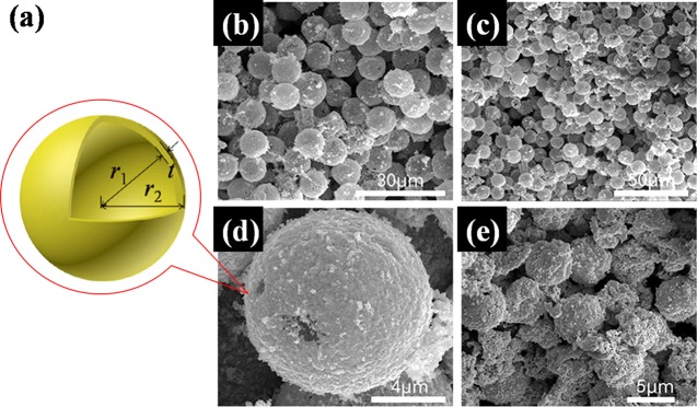
In this work, the foamed Au samples consisted of uniformly dispersed hollow gold microspheres with inner diameter d (d = 2r1) and shell thickness t (t = r2– r1), as shown in Figure 1a. Here, the diameter of the hollow sphere is about d = 10 μm and the Au shell thickness is in the range of about t = 70–90 nm. We find from the bare-eye observation that the color of the samples is nearly black. The diameter of Au hollow sphere can be tuned by using different sizes of polystyrene (PS) microspheres and by electroless plating process to grow different thicknesses of the Au shell. The aperture rate or density of the sample can be controlled by the seed-mediated growth process and by the slip-casting procedure, which can lead to randomly packed Au/PS spheres with void spaces between individual particle units.10 The details of the sample fabrication are presented in Methods. Here, we refer the foamed Au sample to be as a micro/nanoscale hollow sphere structure because the thickness and diameter of the Au shells are in the nano- and micrometer spatial scales, respectively.
Figure 1.
(a) Schematic of hollow gold microsphere. (b–e) Images of formed Au samples, obtained by field emission scanning electron microscopy (FESEM), with different Au hollow sphere diameters d and sample densities ρ. (b) d = 10 μm, ρ = 0.5 g/cm3; (c) d = 10 μm, ρ = 0.6 g/cm3; (d) d = 10 μm, ρ = 0.7 g/cm3; and (e) d = 5 μm, ρ = 0.7 g/cm3.
We take the foamed Au samples with different sample densities (ρ = 0.5, 0.6, and 0.7 g/cm3) and with a fixed Au sphere diameter d = 10 μm for optical measurement. The porosities of these samples are more than 90%. The images of the foamed Au with micro/nanoscale hollow spheres, obtained from field emission scanning electron microscopy (FESEM, S-4800), are shown in Figure 1b–e for different sphere diameters d and sample densities ρ.
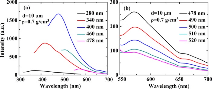
The spectrum of photon-induced light emission is shown in Figure 2a for a sample with a fixed density ρ = 0.5 g/cm3 and a fixed Au hollow sphere diameter d = 10 μm at different excitation wavelengths λex = 280, 340, 400, 460, and 478 nm. As we can see from Figure 2a, the corresponding PL peaks appear at about λem = 372, 417, 472, 511, and 572 nm. Over this excitation wavelength regime, the position of the PL peak depends on pumping wavelength and λem red-shifts with increasing excitation wavelength (λex). Meanwhile, the intensity of the PL spectrum first increases with increasing λex from 280 to 400 nm and then decreases with increasing λex from 400 to 478 nm. These results shown in Figure 2a indicate that when the excitation wavelength is below 478 nm, the intensity and the peak position of the photoemission from foamed Au with micro/nanoscale hollow spheres depend sensitively on the pumping wavelength (λex).
Figure 2.
Photoluminescence spectrum of the foamed gold with micro/nanoscale hollow spheres for different excitation wavelengths. The sample density ρ and the diameter of the Au sphere d are as indicated. The results are shown over the excitation wavelength regime from 280 to 478 nm (a) and from 478 to 520 nm (b).
When we gradually increase the excitation wavelength (λex) in the range of 478–520 nm, we find that the peak position λem in the PL spectrum for the sample is always at about 572 nm, which does not alter markedly with varying the pumping wavelength, as shown in Figure 2b. In this excitation wavelength regime, the intensity of the PL spectrum of the sample decreases monotonously with increasing pumping wavelength. The results shown in Figure 2b indicate that when the excitation wavelength is above 478 nm, the peak position of the photoemission from foamed Au with micro/nanoscale hollow spheres depends very weakly on the pumping wavelength. This implies that over this excitation wavelength regime the photoemission is mainly achieved via typical excitonic light emission mechanism.11
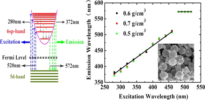
We also carry out measurements for foamed Au with micro/nanoscale hollow spheres at a fixed diameter of the Au hollow spheres d = 10 μm but for different sample densities ρ = 0.5, 0.6, and 0.7 g/cm3. The results are shown in Figure 3, where a fixed excitation wavelength is applied. As we can see, the basic features for the obtained results are very similar to those shown in Figure 2b, except for which we find that the intensity of the photoemission increases markedly with increasing sample density. This effect is due mainly to the fact that a higher sample density corresponds to a larger ingredient of Au material in the sample and, as a result, to a stronger photoemission from Au shell layers. It is known that the macroporosity rate and the existence of spherical voids in the samples are related directly to the sample density. Normally, the higher the sample density is, the lower the macroporosity rate is. Therefore, the results shown in Figure 3 also imply that a sample with a lower macroporosity rate can emit more strongly the PL. Moreover, we find that the difference between the pumping wavelength λex and the peak position λem of photoemission (i.e., λem – λex) is almost independent of the density of the foamed Au samples. Hence, we are able to plot the results for the peak position λem of photoemission against pumping wavelength λex for samples with different densities of foamed Au, which is shown in Figure 4. Interestingly, from Figure 4, we see that over the pumping wavelength regime λex from 280 to 470 nm, the wavelength position of the PL peak λem depends roughly linearly on λex with a slope of about k = 0.75. Thus, in this excitation wavelength range, the wavelength of the photoemission peak can be estimated through λem ≈ a + kλex, with a being about 166 nm, where a and k are obtained by statistical averaging of the experimental data. Furthermore, λem remains at about 572 nm for foamed Au samples with different densities when λex is within the range of 478–520 nm. In this excitation wavelength regime, the PL emission (PLE) occurs mainly through the excitonic mechanism for these samples with different densities, namely, the photoemission is achieved mainly via the combination and separation of the electron–hole pairs in the presence of optical excitation.
Figure 3.
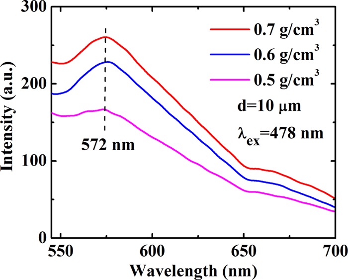
PL spectrum at a fixed excitation wavelength λex = 478 nm for samples with a fixed hollow sphere diameter but with different densities as indicated.
Figure 4.
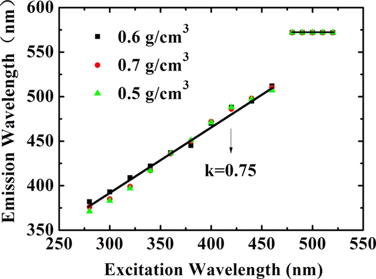
Peak wavelength of the photo-induced light emission λem as a function of excitation wavelength λex for foamed Au samples with different densities ρ as indicated. Here, k is the slope of a roughly linear dependence in shorter pumping wavelength regime. The symbols represent experimental data, and the solid black line is drawn to guide the eye.
It is known that the PL emission via excitonic mechanism is of great importance and significance in understanding the electronic band structure and the electronic relaxation mechanism of an electronic system.11 We therefore would like to focus our attention on the PL emission in the excitation wavelength (λex) range of 478–520 nm. Because the peak position in the PL emission spectrum is at a wavelength λem ∼ 572 nm, which does not vary markedly with altering the pumping wavelength (see Figure 2b), we can perform the PLE measurement on these samples for a fixed emission wavelength. In Figure 5, we plot the intensity of the PLE detected at a fixed light emission wavelength λem = 572 nm against excitation wavelength for samples with different densities. Again, a sample with a larger density can lead to a stronger PLE at a wavelength of about 572 nm for different excitation wavelengths. We notice that two emission peaks can be observed in the PLE spectrum by varying the excitation wavelength: one is at λex ∼ 408 nm and the other is at λex ∼ 478 nm. This interesting finding implies that there are two electronic transition channels or mechanisms responsible for the emission of the PL at a wavelength λem = 572 nm observed experimentally.
Figure 5.
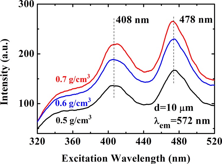
Intensity of PLE at a fixed emission wavelength λem = 572 nm as a function of excitation wavelength for samples with different densities as indicated. Two peak wavelengths are indicated.
Now we discuss the physical mechanism behind the experimental findings shown in Figures 2–5 for foamed Au with micro/nanoscale hollow spheres.12 We know that gold is a monovalent metal, which belongs to the face-centered cubic lattice structure with a shell structure being as [Au] 5d10–6sp1. The atomic structure of Au is quite similar to that of the alkali metals, but Au has the s-orbit near the d-orbit. It is known12 that when gold atoms form into the Au solid with a lattice structure, the s-orbits in Au evolve into a wide s-band due to large overlap of the electron wave functions, whereas the d-orbits evolve into a narrow d-band due to the effect of the localization. For the case of Au-based micro/nanoscale hollow sphere structures, because the thickness of the Au shell is on the nanometer scale, the quantum size effect takes place so that the corresponding energy band can be quantized into the electronic sub-bands.13 As a result, the visible fluorescence from Au-based micro/nanoparticles is attributed mainly to interband electronic transitions between the 6sp1 conduction-like band and the 5d10 valence-like levels.14 From the results obtained from this study, we are able to construct an energy-level diagram and possible electronic transition channels accompanied by the absorption and emission of photons for foamed gold with micro/nanoscale hollow sphere structure, which is shown in Figure 6. In the presence of excitation light field, the electrons in the 5d10 valence-like band are pumped into the 6sp1 conduction-like band via the optical absorption mechanism (blue lines in Figure 6). There are two major channels or mechanisms for radiative relaxation of photoexcited electrons in the 6sp1 band as follows.
Figure 6.
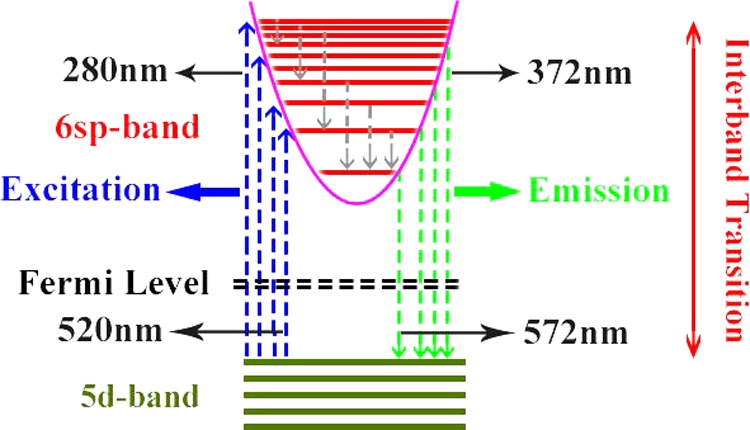
Schematic diagram of the energy states for Au hollow sphere structure and the corresponding electronic transition channels for optical excitation (blue lines), nonradiative electronic relaxation (gray lines), and photo-induced light emission (green lines).
The first channel or mechanism for photon-induced light emission is the direct photoemission induced by electronic transitions from higher energy levels to lower energy states. As we know, the electrons in the higher energy states have normally a quicker (shorter) relaxation time than those in the lower energy states. For the case of relatively short-wavelength excitation, the photon-induced light emission from foamed Au is mainly achieved through this mechanism. The photoexcited electrons in the higher energy states in the 6sp1 band first quickly relax into the lower energy states via nonradiative intraband relaxation mechanism, such as electron–phonon scattering and electron–electron interaction (gray lines in Figure 6). When the nonradiative electronic relaxation time for electrons in the 6sp1 states is longer or larger than the radiative electronic relaxation time, these electrons can go back to the 5d10 band and emit photons (green lines in Figure 6). With decreasing pumping wavelength, more states in the 5d10 band and especially in the 6sp1 band can take part in these pumping, relaxation, and emission processes and thus the peak wavelength in the light emission spectrum decreases with excitation wavelength. Therefore, the wavelength of the light emission depends on the excitation light wavelength. The roughly linear increase in the peak wavelength of light emission with excitation wavelength implies that the nonradiative electronic relaxation time increases almost linearly with lowering energy levels in the 5d10 band for electrons in foamed Au, as observed in this study.
The second channel or mechanism for photon-induced light emission from foamed Au is the excitonic mechanism.10 When electrons in the 5d10 band are pumped optically into the 6sp1 states, the holes are generated in the 5d10 band and the excitons or electron–hole pairs induced by electron–hole interaction due to Coulomb potential can be formed in the sample system. By this mechanism, the photoexcited electrons in the high energy states in the 6sp1 band are relaxed into the low energy states via nonradiative intraband electronic transition channels and these electrons are combined with the holes in the 5d10 band to form the excitons. The separation of the electron–hole pairs can lead to the emission of light with the peak wavelength corresponding to the energy gap between the 6sp1 and 5d10 bands. Because this energy gap does not change with pumping wavelength, the peak wavelength of the PLE from foamed Au does not vary with the pumping wavelength. For the case of relatively long-wavelength excitation, the PLE from foamed Au is mainly achieved through this mechanism. The result obtained from this study suggests that the energy gap between the 6sp1 and 5d10 bands in foamed Au with micro/nanoscale hollow spheres is about 527 nm or 2.35 eV, which is much larger than 1.48 eV measured from the PL for Au nanoparticles4 with 488 nm argon-ion laser pumping. The main reason why the foamed Au with nanoshells has a larger energy gap than that in Au nanoparticles is that the stronger quantum size effect can be achieved in the nanoshell structure,13 which can enhance the energy spacing between the lowest sub-band in the 6sp1 band and the highest sub-band in the 5d10 band. It should be noted that a relatively sharp PL peak was observed for Au nanoparticles,4 whereas the rather broad-band PLE can be seen for foamed Au with micro/nanoscale hollow spheres. Therefore, the basic features of PLE from foamed Au materials differ significantly from those observed for Au nanoparticles. Moreover, in contrast to single-wavelength optical pumping to measure the PLE for Au nanoparticles,4 here we are able to conduct the measurements via varying the excitation wavelength so that the emission via excitonic mechanism can be confirmed and verified.
It should be noted that the two light emission channels or mechanisms discussed above for foamed Au are competitive. When electronic relaxation time for direct light emission is shorter than excitonic lifetime, wavelength-dependent light emission can be observed, and vice versa. Because the higher energy states in the 6sp1 band normally have shorter electronic lifetime, the wavelength-dependent light emission can be observed with shorter wavelength pumping, whereas the PLE via excitonic mechanism can be seen with relatively longer-wavelength pumping. The results obtained from this study suggest that 478 nm excitation wavelength is a critical point between two mechanisms. Namely, the electronic relaxation time for energy states above this level is shorter than excitonic lifetime so that the direct light emission can be observed, whereas the excitonic lifetime for energy states below this level is shorter than nonradiative electronic relaxation time so that the PLE can be observed.15 Furthermore, a larger density of the sample means more sources of photo-emission. This is the main reason why the intensity of the PL emission from foamed Au with micro/nanoscale hollow spheres increases with sample density, as shown in Figures 3 and 5.
It is reported that PL emission in noble-metal-nanoparticles can enhanced by the presence of the plasmon locla field effect.15 However, although the foamed Au samples consist of micro/nanoscale hollow Au spheres, we have not observed explicit resonant optical phenomena associated with localized surface plasmons (LSPs) during the photo-induced light emission measurements in the visible regime. As we know, the LSPs supported by metallic nanoshell are usually thought to arise via the hybridization of the dipolar modes of a metallic sphere and a corresponding dielectric void in a metal substrate.16 This kind of hybridization in the nanoshell geometry can lead to both shifts of the plasmon frequencies into the long-wavelength region (such as the near-infrared region) and reduced plasmon linewidth, when both the inner and outer radii of the shell are in the subwavelength scale. The scattering from the nanoshells with subwavelength inner and outer radii can provide light with wave vector components in a broad range,16 which leads to effective hybridization of the dipolar plasmon modes of metallic spheres and dielectric inner voids. However, in the present study, r1 and r2 of the hollow spheres are nearly 16–35 times larger than the excitation or emission wavelength (i.e., r1, r2 ≫ λex, λem). Therefore, it is very difficult to excite dipolar modes in very large spheres and inner voids to further generate localized plasmonic resonances (such as LSPs) effectively, even if there may be a few subwavelength defects and cracks in the Au nanoshells. In other words, the efficiency of the plasmonic excitations of the hollow spheres is too low to cause obvious resonant phenomena in the visible range.
Moreover, due to the casting procedure in the sample fabrication, the arrangement of the hollow gold microspheres is disordered, which also means disordered arrangement of the voids both inside and outside the nanoshells. It should be noted that the disordered voids outside the nanoshells can act as disordered cavities with random sizes, which corresponds to random resonant wavelengths in a broad range. Thus, the joint effect of the strong random absorption in these disordered cavities and the diffuse reflections on the rough sphere surfaces can give rise to broad-band absorbance. It is responsible for the weak reflection spectra submerged in background noise when we performed the conventional light reflection experiment. Another obvious evidence of this kind of broad-band absorption in visible bandwidth is that the color of the samples is nearly black from the bare-eye observation. Moreover, the number of hollow gold spheres on top of each other may affect the corresponding optical properties of the samples. At present, it is difficult to control the stacked number and order of the disordered hollow spheres in the foamed Au structure via current sample fabrication technique.
Although we have not prepared flat Au films via electroless plating, we believe that the basic PLE behavior of the thin Au film does not depend on the method of fabrication. Thus, the results of our foamed Au materials can be compared to the results of Au films obtained in previous works. It should be noted that in visible bandwidth normally there is only one typical PL peak to be observed in Au thin films (see, e.g., Figure 2 in ref (17)), for which the peak position does not vary with excitation wavelength. This corresponds to the direct optical transition between s- and d-bands in Au. As for Au nano/macrosphere array structures, two PL peaks can be observed:6 one corresponding to the band gap between s- and d-bands and the other to the pattern of the array structure. The experimental results shown and discussed in this work indicate that the basic features of the PLE from foamed Au materials with micro/nanoscale hollow sphere structures differ significantly from those in flat Au films and Au nanosphere arrays. Moreover, by comparing the results measured for Au mirror, Au nano/macrosphere array structures,6 and foamed Au materials, we find that generally larger PL intensities can be observed in Au mirror and Au nano/macrosphere array structures. A relatively weak PL intensity can be measured for foamed Au materials. This implies that the quantum yield of the light emission from foamed Au materials with micro/nanoscale hollow sphere structures is lower than that from Au mirror and Au nano/macrosphere array structures.
Conclusions
In this study, we have fabricated the macroscale and monolithic foamed Au materials with micro/nanoscale hollow sphere structures, which is a new class of Au-based micro/nanostructure. The basic features of photon-induced light emission from these samples with different densities have been examined. The main conclusions obtained from this study can be summarized as follows.
The strong and characteristic light emission from foamed Au materials with micro/nanoscale hollow sphere structures can be observed in the presence of optical excitation. In a relatively short-wavelength excitation regime (280–470 nm), the peak position in the photoemission spectrum increases almost linearly with excitation wavelength. This effect is mainly induced by direct photon emission when electronic relaxation time in high energy states in the 6sp1 band is shorter than excitonic lifetime in low energy states. In a relatively long-wavelength excitation regime (478–520 nm), the PLE can be observed where the peak position in the PL spectrum depends very little on excitation wavelength and two peaks can be seen in the emission spectrum. In this excitation wavelength regime, the PLE from foamed Au is achieved mainly via excitonic mechanism. We have found that the energy gap between the 6sp1 and 5d10 bands in our samples is about 527 nm or 2.35 eV. These important features do not change significantly with varying sample density, although it has been found that the intensity of the light emission increases with sample density. The results presented and discussed in this article indicate that the features of the photo-induced emission from foamed gold with micro/nanoscale hollow spheres differ significantly from those observed for Au nanoparticles. For foamed Au with hollow micro/nanosphere structural units, the corresponding optoelectronic properties can be tuned by varying sample parameters, such as the diameter of the hollow Au microsphere, the nanoscale thickness of the Au shell, and the aperture rate or density of the sample. We hope the interesting and important findings from this study can help us to gain an in-depth understanding of the basic optical properties of the macroscale and monolithic foamed Au materials with micro/nanoscale hollow sphere structures and to provide significant information about the application of Au micro/nanostructures as advanced optoelectronic materials and devices.
Methods
Sample Fabrication
The macroscale and monolithic foamed Au materials with micro/nanoscale hollow sphere structure are fabricated through the main process, as shown in Figure 7. (i) The gold particles with average grain size of about 4.6 nm are made in toluene by the electrostatic technique. They can be adhered and coated on the surface of PS microspheres with a diameter r1. (ii) The Au particles coated on the surface of the PS microspheres are taken as seed crystals for electroless plating to grow the Au shell layers. The deposited gold with thickness of about 70–90 nm and grain size of about 30–60 nm can be obtained. The diameter of the spheres with Au shell is r2, and the thickness of the Au shell is t = r2 – r1. (iii) The reducing agent is kept on the surface of the seeds on deoxidizing HAuCl4 to make the gold plating layer continue to grow thicker. This step is followed by a casting procedure analogous to slip casting of ceramic. This procedure can result in randomly packed PS/Au spheres with void spaces between individual particles. Thus, the arrangement or pattern of the hollow gold microspheres obtained in the structure is normally not ordered in contrast to the usual fabrication of nanoarray structure based on PS particle templates. (iv) The PS spheres inside the Au shells are removed by further heat treatment under nitrogen atmosphere and at a temperature of about 400 °C. After removing the PS microspheres, the Au shells are self-supported with reasonable mechanical strength. Using this technique, the monolithic foamed gold with disordered and self-supported hollow microspheres can be directly obtained in the macroscale size, in contrast to the conventional layer-by-layer growth method. The sample obtained in the present study is a black-looking cylinder with both diameter and height of about 4 mm. In these samples, the diameter of the hollow sphere is about d = 10 μm, which is decided by the size of the PS microsphere seed, and the Au shell thickness t can be controlled in the range of about 70–90 nm corresponding to different densities (ρ = 0.5, 0.6, and 0.7 g/cm3). In this study, the sample density is estimated by ρ = M/V, with M being the measured mass and V being the volume calculated by sample diameter and height. More detailed information about the synthesis process can be found in ref (10).
Figure 7.
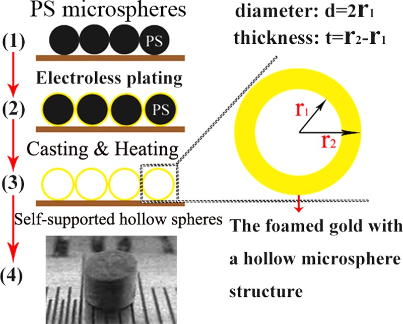
Flow chart for the preparation of foamed gold material with micro/nanoscale hollow spheres. Here, r1 is the radius of the PS sphere, t = r2 – r1 is the thickness of the Au shell, and d is the diameter of the hollow sphere. In step (4), the photo of the sample is shown. It is important to note that it is only a schematic of the sample fabrication process here. The details of the process are presented in Methods.
PL Emission Measurements
We take a standard experimental setup to measure the photo-induced light emission from foamed Au samples with micro/nanoscale hollow spheres in visible bandwidth. The HORIBA fluorescence system is applied for the measurement, where a xenon lamp is taken as broad-band excitation light source, the GEMIMI 180 monochromator is used for choosing the pumping wavelength, and the iHR320 grating spectrometer together with a photoelectric multiplier tube detector is used for recording the spectrum of the light emission from samples. The excitation light beam is applied at an angle of about 45° to the sample surface, and the detection is undertaken at about 60° to the sample surface. The accuracy of the measurement system can be up to 0.2 nm in optical wavelength, and the measurements are carried out at room temperature.
Acknowledgments
This work was supported by the National Natural Science Foundation of China (11574319 and 11304272), the Ministry of Science and Technology of China (2011YQ130018), the Hefei Center of Physical Science and Technology, the Department of Science and Technology of Yunnan Province (2013FD003 and 2016FC001), and the Chinese Academy of Sciences.
The authors declare no competing financial interest.
References
- Ji K.; Xu Y.; Zhang J.; Chen J.; Dai Z. Foamed-metal-reinforced composites: Tribological behavior of foamed copper filled with epoxy–matrix polymer. Mater. Des. 2014, 61, 109–116. 10.1016/j.matdes.2014.04.072. [DOI] [Google Scholar]
- Young P. E.; Rosen M. D.; Hammer J. H.; Hsing W. S.; Glendinning S. G.; Turner R. E.; Kirkwood R.; Schein J.; Sorce C.; Satcher J. H.; Hamza A. Jr.; Reibold R. A.; Hibbard R.; Landen O.; Reighard A.; McAlpin S.; Stevenson M.; Thomas B. Demonstration of the Density Dependence of X-Ray Flux in a Laser-Driven Hohlraum. Phys. Rev. Lett. 2008, 101, 035001 10.1103/PhysRevLett.101.035001. [DOI] [PubMed] [Google Scholar]
- Rosen M. D.; Hammer J. H. Analytic expressions for optimal inertial-confinement-fusion hohlraum wall density and wall loss. Phys. Rev. E 2005, 72, 056403 10.1103/PhysRevE.72.056403. [DOI] [PubMed] [Google Scholar]
- Schasfoort R. B. M.; Tudos A. J.. Handbook of Surface Plasmon Resonance; RSC Publishing: U.K., 2008; pp 15–31. [Google Scholar]
- Lin A.; Son D. H.; Ahn I. H.; Song G. H.; Han W.-T. Visible to infrared photoluminescence from gold nanoparticles embedded in germano-silicate glass fiber. Opt. Express 2007, 15, 6374. 10.1364/OE.15.006374. [DOI] [PubMed] [Google Scholar]
- Zhang Y. Y.; Xiao Y. M.; Duan G. T.; Su F. H.; Cai W. P.; Xu W. Optical Properties of Gold Nanosphere Arrays Formed on Polystyrene Templates. Integr. Ferroelectr. 2012, 136, 66–70. 10.1080/10584587.2012.686784. [DOI] [Google Scholar]
- Wang J.; Zhang C.; Zhang J.; Song H.; Wang P.; Lu Y.; Fei G.; Xu W.; Xu W.; Zhang L.; Kivshar Y. S.; Zhang L. Hybrid Plasmonic Cavity Modes in Arrays of Gold Nanotubes. Adv. Opt. Mater. 2017, 5, 1600731 10.1002/adom.201600731. [DOI] [Google Scholar]
- Zhu J.; Li J.-j.; Zhao J.-w. The Study of Surface Plasmon Resonance in Au–Ag–Au Three-Layered Bimetallic Nanoshell: The Effect of Separate Ag Layer. Plasmonics 2014, 9, 435–441. 10.1007/s11468-013-9640-9. [DOI] [Google Scholar]
- Nakaji K.; Li H.; Kiba T.; Igarashi M.; Samukawa S.; Murayama A. Plasmonic enhancements of photoluminescence in hybrid Si nanostructures with Au fabricated by fully top-down lithography. Nanoscale Res. Lett. 2012, 7, 629. 10.1186/1556-276X-7-629. [DOI] [PMC free article] [PubMed] [Google Scholar]
- Xiulan T.; Gao N.; Kai L.; Lou J.; Weidong W.; Yongjian T. Preparation of Monolithic Foamed Gold by Seed-Mediated Growth. Rare Met. Mater. Eng. 2012, 41, 169–172. [Google Scholar]
- Siwach O. P.; Sen P. Synthesis and study of fluorescence properties of Cu nanoparticles. J. Nanopart. Res. 2008, 10, 107–114. 10.1007/s11051-008-9372-5. [DOI] [Google Scholar]
- Mooradian A. Photoluminescence of Metals. Phys. Rev. Lett. 1969, 22, 185. 10.1103/PhysRevLett.22.185. [DOI] [Google Scholar]
- Xiao Y.; Xu W.; Zhang Y.; Hu J. Terahertz plasmon and surface-plasmon modes in hollow nanospheres. Nanoscale Res. Lett. 2012, 7, 578. 10.1186/1556-276X-7-578. [DOI] [PMC free article] [PubMed] [Google Scholar]
- Huang T.; Murray R. W. Visible luminescence of water-soluble monolayer-protected gold clusters. J. Phys. Chem. B 2001, 105, 12498–12502. 10.1021/jp0041151. [DOI] [Google Scholar]
- Shahbazyan T. V. Theory of Plasmon-Enhanced Metal Photoluminescence. Nano Lett. 2013, 13, 194. 10.1021/nl303851z. [DOI] [PubMed] [Google Scholar]
- Maier S. A.Plasmonics: Fundamentals and Applications; Springer: New York, 2007; pp 65–87. [Google Scholar]
- Vengurlekar A.; Ishihara T. Photoluminescence in Au film: Enhanced emission for a corrugated film. J. Lumin. 2007, 122–123, 796–799. 10.1016/j.jlumin.2006.01.291. [DOI] [Google Scholar]


