Abstract
The electronic, transport, optical, thermoelectric, and thermodynamic properties of the two-dimensional (2D) stable monolayer of boron arsenide (BAs) sheets have been investigated using state-of-art theoretical calculations. The energetic, dynamic, thermal, and mechanical stability of the BAs sheet have also been studied to unravel the feasibility of experimental realization of this material. Interestingly, the band gap of this semiconducting sheet changes from direct into indirect band gap material by the application of biaxial strain of 10% and it becomes metallic at 14% of biaxial strain. Furthermore, positive phonon vibrational modes have been observed for all applied biaxial strains, which ensure the stability of the sheet under strain. The semiconducting property is preserved when cutting 2D sheet into one-dimensional nanoribbons, and the band gap is size dependent. In addition, the calculated optical properties exhibit strong anisotropy. BAs nanomaterial has strong adsorption in the UV–visible region. The calculated Seebeck coefficient and power factor values show that BAs sheet is an ideal candidate for thermal management and thermoelectric applications. Finally, the thermodynamic properties have been calculated on the basis of the phonon frequencies. These rich properties of BAs nanosheets endow the system with promising applications in nanoelectronics and photovoltaics.
Introduction
The invention of graphene,1 h-BN,2 transition-metal dichalcogenides3,4 (TMDC), and other two-dimensional (2D) materials5−8 has triggered tremendous interest in the field of nanoscience and technology. The promising potential applications of these materials are well documented in recent studies.9−17 Typically, graphene has an excellent electron mobility,18 which makes graphene a superior candidate in transistor and other applications. These 2D materials have been used to recognize various biomolecules,19,20 pollutants,21,22 and gas molecules23,24 to develop suitable sensing devices. However, the usefulness of these materials is limited because of lack of band gap in graphene,25 large band gap in h-BN, and lower carrier mobility in TMDC,26 which calls for further development of alternative materials that can be used in a variety of fields. Chemical doping,27 noncovalent interactions of various molecules,28 and structural engineering by cutting 2D sheets into nanoribbons (NRs) are some of the possible ways to engineer the band gap of graphene. However, the opening of the band gap significantly reduces the conductivity. Hence, searching for novel 2D semiconducting materials endowed with required electronic properties is utmost important for multifunctional applications.
Şahin et al.29 proposed 22 materials having honeycomb lattice that are composed of groups IV and III–V elements. These materials are found to be minimum on the Born–Oppenheimer surface. Among these proposed materials, few of them are experimentally synthesized30,31 and their potential applications have been well explored.32,33 However, some of the materials are yet to be synthesized and their applications in various fields have not been unraveled. In this context, boron arsenide (BAs) sheet has been chosen from a list of materials that are yet to be synthesized for the current investigation. There are specific reasons for choosing BAs for the present study: (i) cubic boron arsenide has been synthesized,34,35 and its properties have also been determined (predicted) from experimental (theoretical) methods.36 It was found that cubic BAs have very high thermal conductivity, which is comparable to that of diamond and graphite.36 (ii) In the family of III–V compounds, BAs have the highest covalent character37 and are stable against chemical decomposition and dissolution.38 (iii) Another exciting feature is that the valence bands of BAs can offset those of GaAs,39 which makes these materials as ideal alloying systems. These interesting properties prompted us to explore further electronic, transport, optical, and thermoelectric properties of BAs sheets.
In the present study, an extensive analysis on the structure and stability of 2D hexagonal BAs sheet has been carried out by employing first principles density functional theory (DFT)-based periodic calculations. The following important points have been investigated:
-
(i)
To unravel the effect of application of biaxial strain on the electronic properties of BAs sheet.
-
(ii)
To understand the effect of nanoconfinement on the electronic properties of BAs sheet by designing appropriate one-dimensional (1D) zigzag nanoribbon (ZNR) and armchair nanoribbon (ANR).
-
(iii)
To explore the potential multifunctional applications of this novel material by computing electronic, transport, optical, thermoelectric, and thermodynamic properties.
Results and Discussion
Geometrical Properties
The stable structure of a honeycomb lattice consisting of two atoms B and As is shown in Figure 1. This material belongs to P6̅M2(D3H1) symmetry with hexagonal space group (space group no. 187). The optimized lattice parameters of BAs are a = b = 3.39 Å with B–As bond length of 1.95 Å and bond angle of 120°. These values are in good agreement with the previously reported values.40,41
Figure 1.
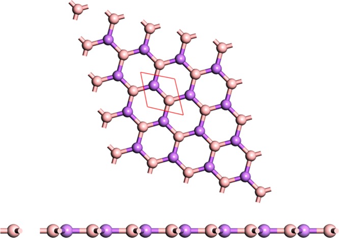
Top and side view of a planar boron arsenide sheet.
To elucidate the nature of chemical bonding in BAs sheet, electron localization function (ELF)42 was calculated and the contour map sliced perpendicular to the (001) direction is shown in Figure 2. ELF is a measure of relative electron localization in the structure, where the value 1 (red) denotes the fully localized electrons, 0 (blue) indicates typically low electron density area, and 0.5 implies the probability of free electron gas. It can be clearly seen from Figure 2 that high localization of electron can be observed in the middle of the B–As bond, reflecting the role of strong covalent bond in the stabilization of this material.
Figure 2.
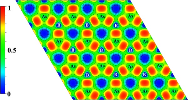
Calculated ELF contour map sliced perpendicular to the (001) direction.
It is well known that the cohesive energy determines the stability of the material. The cohesive energy of BAs sheet has been calculated using the following equation
where ECoh is the cohesive energy (per atom), EBAs is the total energy of the unit cell, EB and EAs are the the energy of the isolated elements, and nB and nAs are the number of atoms in the unit cell. The calculated cohesive energy is found to be −4.29 eV/atom, which implies the stability of the system. The calculated ECoh is also in close agreement with previously reported values.41 The cohesive energy of arsenene, AsP, AsSb, AsBi, and AsN are −2.953, −3.153, −2.771, −2.642, and −3.443 eV/atoms, respectively.43,44 It can be noticed that the calculated cohesive energy is comparatively higher than that of the arsenene sheet and its alloys. Some of the cohesive energies of other theoretically predicted 2D materials, such as CdS (−2.65 eV/atom),45 GeS (3.01 eV/atom),46 GeSe (2.77 eV/atom),46 SnS (2.06 eV/atom),46 and Cu2As (2.98 eV/atom),47 have been reported. Ding et al.48 concluded that SiX and XSi3 (X = B, C, N, Al, and P) can possibly be synthesized by chemical vapor deposition and molecular beam epitaxy methods on the basis of cohesive energy calculations. On the basis of similar arguments, BAs sheet is also an experimentally realizable material.
Dynamic Stability
In general, the phonon calculation is an appropriate approach to investigate the dynamical stability of materials. The calculated phonon dispersion curve and phonon density of states (PDOS) of BAs sheet are are displayed in Figure 3a,b. It can be seen from Figure 3a, there is no imaginary mode in the phonon dispersion indicating the inherent dynamical stability of the system and confirming that BAs sheet is indeed a local minimum. Notably, the highest frequency of the BAs monolayer is 834 cm–1, which is higher than that of arsenene allotropes, silicene (580 cm–1),49 tetrasilicene (466 cm–1),50 hexasilicene (560 cm–1),49 MoS2 monolayer (473 cm–1),51 and phosphorene (∼450 cm–1)52 materials, which indicates the higher strength of B–As bond.
Figure 3.
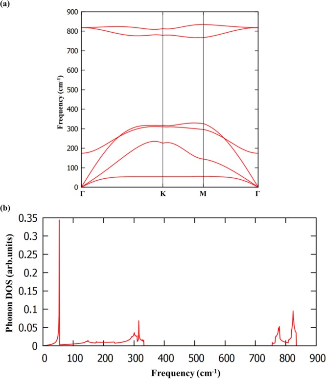
(a) Calculated phonon dispersion curve and (b) phonon density of states of BAs.
Thermal Stability
The thermal stability of BAs sheet is assessed by performing ab initio Born–Oppenheimer molecular dynamics (BOMD) simulations in which the forces are calculated from the ground-state electronic configuration at each molecular dynamics step. The CASTEP53 package was used as implemented in Material studio. The total simulation time of 5 ps with a time step of 1 fs in NVT ensemble was performed at 300 K. It is noted from Figure 4a that the material is stable at room temperature with negligible deviation from the planarity. The total energy profile as a function of time is shown in Figure 4b. The mechanical stability of the BAs sheet has been assessed by calculating the elastic constant using thermo_pw module, as implemented in Quantum ESPRESSO.54 The computed elastic constants fulfill the Born criteria55 of stability for hexagonal structures, i.e., C11 > 0 and C11 – C12 > 0 and C66 > 0, which ensures the mechanical stability of the system. The calculated values of C11, C12, and C66 are 80.65, 19.71, and 29.09 GPa, respectively, and provide valuable information on the strong bonding.
Figure 4.
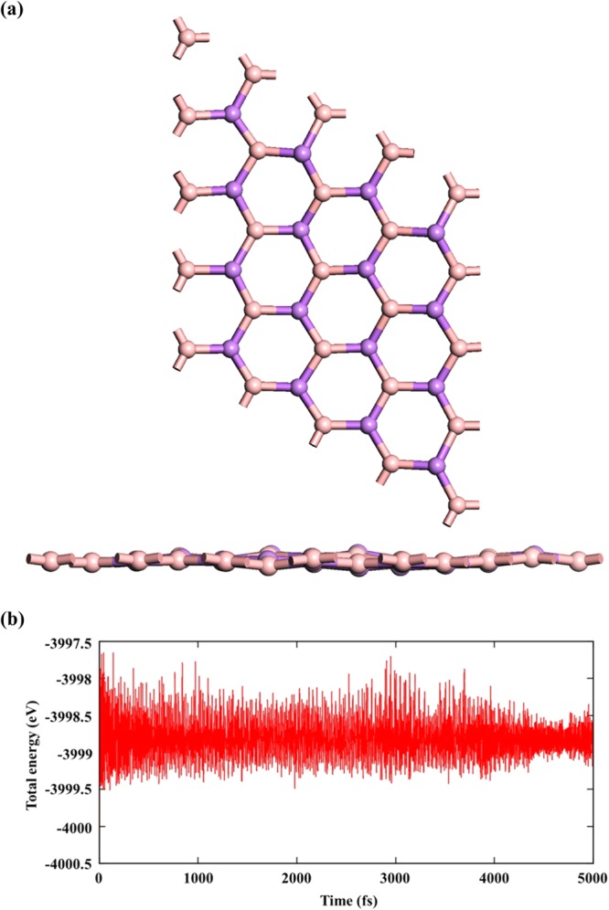
(a) Top and side view of a BAs sheet at 300 K and (b) calculated total energy as a function of time.
Therefore, our findings from cohesive energy calculations, phonon dispersion, and BOMD simulations highlight that the BAs sheet is stable and there is a high possibility that this can be experimentally realizable.
Electronic Properties
The calculated band structure of BAs sheet is presented in Figure 5. It can be observed from Figure 5 that it is a direct band gap semiconductor, with a band gap of 0.76 eV. Both valence band maximum (VBM) and conduction band minimum (CBM) are located at the K point. The contributions of individual orbitals of a BAs sheet can be observed from PDOS. The VBM are mainly contributed by p orbitals of arsenene, and CBM are contributed by p orbitals of boron. This appreciable band gap would facilitate the application of BAs sheet in nanoelectronics, as observed in other similar 2D materials. We have also calculated the Lowdin charges, and it is noted that 0.49e is transferred from arsenene to boron atom.
Figure 5.
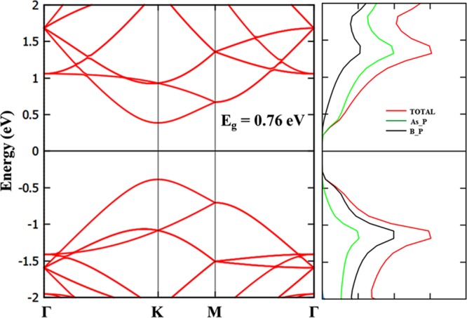
Calculated band structure and PDOS of BAs sheet.
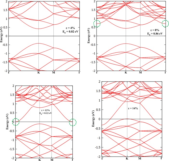
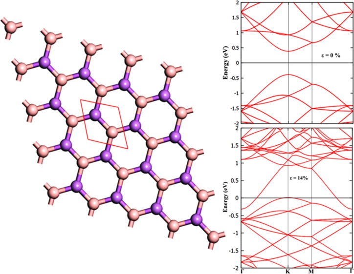
Application of strain on materials is one of the effective ways to engineer the electronic properties of 2D materials. The effect of biaxial strain on the electronic properties of a BAs sheet (schematic representation as shown in Figure 6a) has been studied by applying strain (ε) from 2 to 14%. During the application of strain, the prediction of stability of material is primarily important. Hence, the phonon dispersion calculations have been performed to unravel the stability of this material for various values of applied strain. The predicted phonon dispersion results are presented in Figure 6b,c. It can be noticed from phonon dispersion and associated phonon density of states in Figure 6b,c that there are no imaginary vibrational modes, implying BAs sheets possesses high mechanical strength and are dynamically stable under strained conditions up to ε = 14%. As observed from Figure 6b,c, frequencies of all phonon modes soften considerably under strain due to stretching of the bonds.56 The calculated band structure of BAs sheet under various biaxial strains is depicted in Figure 7. This material behaves as a direct band gap semiconductor for up to 8% of strain, and the increase in the band gap is marginal (Supporting Information, SI (Figure S1)). The change in the band gap takes place from direct to indirect band gap by the employment of 10% strain, and the band gap value is found to decrease. The material becomes metallic by the application of biaxial strain of 14%. The conduction band has a tendency to approach the Fermi level by the application of biaxial strain (say 10% in BAs sheet). Thus, the inherent direct band gap semiconducting nature of BAs changes to indirect band gap material by the application of 10% strain and it becomes metallic upon employment of 14% biaxial strain.
Figure 6.
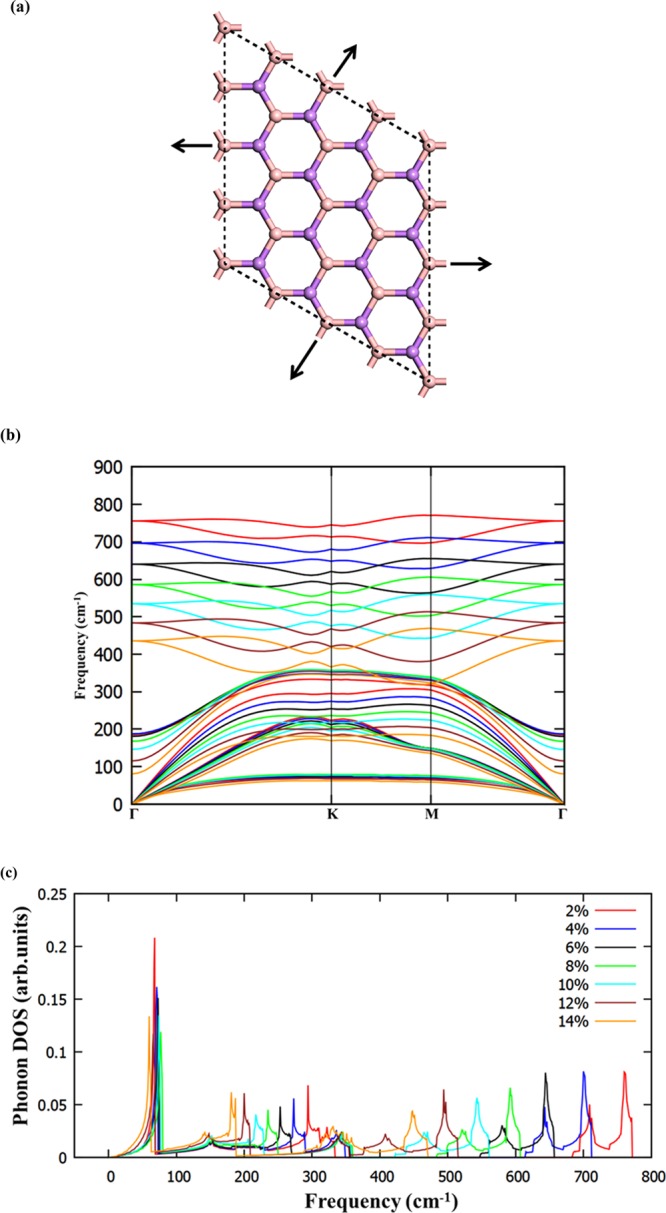
(a) Schematic representation of BAs with biaxial strain, (b) calculated phonon dispersion curve, and (c) phonon density of states of a BAs sheet with various values of applied biaxial strain.
Figure 7.
Strain-induced electronic band structure of a BAs sheet with different biaxial strains.
We have also modeled the 1D nanoribbons (NRs) by cleaving the BAs sheet along (110) and (100) directions to get armchair nanoribbon (ANR) and zigzag nanoribbons (ZNRs) (SI Figure S2), respectively. The edges of the nanoribbons are passivated by hydrogen atoms to saturate B and As atoms. To investigate the effect of nanoconfinement on the electronic structure of nanoribbons, we have increased the width (N) of the ribbons from N = 1 to 7. The computed band structures are shown in SI Figure S2. Both zigzag and armchair nanoribbons elicit a semiconducting character, and with increase in the width, the band gap of the nanoribbons decreases. When compared to the ZNR, the band gap of ANR is high (up to N = 3). However, N = 4 onward the band gaps of the both systems are almost equal.
Transport Properties
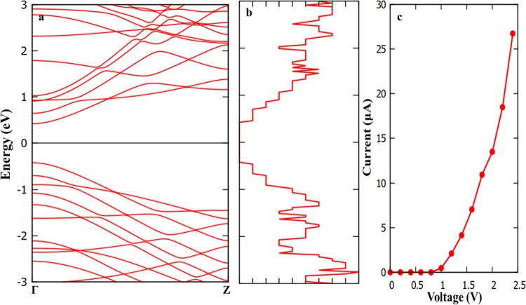
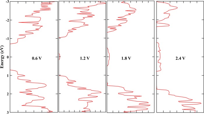
We have used nonequilibrium Green’s function technique combined with DFT approach, as implemented in TranSIESTA57 package to study the transport characteristics of BAs nanoribbon. A two-probe model was used, in which semi-infinite left and right electrodes were connected with the scattering region, as shown in Figure 8. Both scattering and electrode regions are made with 11 ANR. The scattering regions contain four primitive unit cells with the length of 23.52 Å. To provide a better understanding of the transport phenomena, the band structure of the electrode/scattering of their primitive unit cell is displayed in Figure 9a. It is observed from Figure 9a that, it is a direct band gap semiconductor with the band gap value of 0.84 eV. The calculated zero bias transmission spectra is shown in Figure 9b, which is consistent with the computed band structure. We have calculated the current (I) as a function of applied bias voltage (V), which is represented in Figure 9c. The calculated I–V curve clearly supports the computed band structure and transmission spectra. As observed from Figure 9c, the device has a threshold voltage (Vth) of 0.8 V, below which the current is close to zero and above which the current tends to increase. Further increasing V (say above 0.8 V), the corresponding output current increases. The effect of increase in the current can be comprehensively understood from the calculated transmission spectra with various values of V, as given in Figure 10. The following important observations emerge from the close analysis of the variation of current with bias voltage: (i) the BAs nanoribbon has a conductance gap of 0.8 V at zero bias voltage. (ii) Upon increasing the bias voltage above the threshold value, the valence band of the left electrode matches the energy of the conduction band of the right electrode. Hence, tunneling of electrons takes place through the valence band of the left electrode to conduction band of the right electrode. (iii) Thus, the conductance band gap decreases with the increase in the bias voltage and leads to increase in the associated current. Further, we have calculated the I–V characteristics to understand the effect of size and length of the scattering region of the nanoribbons and results are depicted in SI Figures S4 and S5.
Figure 8.
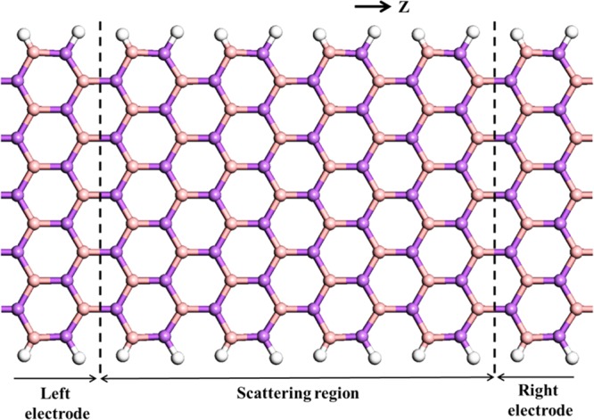
Schematic representation of the device model constructed with armchair nanoribbon. The periodic direction is Z.
Figure 9.
(a) Band structure of armchair nanoribbon, (b) zero bias transmission spectra, and (c) I–V curve.
Figure 10.
Transmission spectra under various bias voltages.
Optical Properties
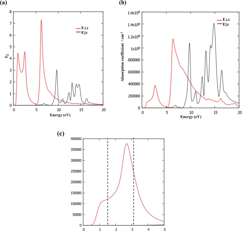
The direct band gap nature of this material has multifunctional applications in the field of optical devices due to the formation of exciton that requires less energy. From an experimental point of view, the optical properties are determined by the luminescence spectrum, absorption coefficient, reflection and refraction index, and electron energy loss spectroscopy. All of these measurable optical properties can be evaluated by the calculation of dielectric functions. The calculated imaginary part (ε2) of the dielectric function with the electric field parallel (E || c) and perpendicular (E ⊥ c) to the basal plane of a BAs sheet is presented in Figure 11a. The anisotropic behavior in parallel and perpendicular polarizations of the electric field can be seen from Figure 11a. There are two strong optical absorption regions in the range 0.7–5.2 and 5.3–10 eV. These values cover near-IR, visible, and UV regions of the electromagnetic spectrum. The first exciton peak of BAs corresponding to E ⊥ c is found to be at 0.7 eV. The second exciton peak occurs at 2.1 eV, and the third exciton peak appears at 5.5 eV. If the electric field polarization is parallel to the c direction, there is no major peak corresponding to the imaginary part of the dielectric function up to 8.5 eV, indicating negligible optical absorption in this region. Hence, the intensity of ε2 in perpendicular (E ⊥ c) polarization is larger than that in parallel (E || c) polarization. Thus, it is evident from the optical properties of a BAs sheet that it behaves as an anisotropic material. The calculated absorption coefficient of a BAs sheet is shown in Figure 11b. The strong absorption appears in the UV range, and an intense peak appears at 6.4 eV for E ⊥ c. For parallel polarization, the absorption coefficient of BAs sheet is almost negligible in the visible region (completely opaque to the visible region) and it has a strong absorption characteristic for a UV region with many peaks. These results are in concomitance with the calculated ε2 values. We are particularly interested in focusing on the absorption coefficients in the visible ranges for applications in optical devices. It is observed from Figure 11c that a relatively strong absorption peak with a value of 2.6 eV in the visible-light range is observed. Thus, it can be clearly noticed that this material can also absorb low-energy light quite effectively, indicating BAs sheets can be employed as a potential material for the development of short-wavelength optoelectronic devices for energy conversion and UV-light protection.
Figure 11.
(a) Calculated dielectric function of BAs sheet for parallel and perpendicular electric fields, (b) absorption coefficient, and (c) absorption coefficient in the visible regions.
Thermoelectric Properties
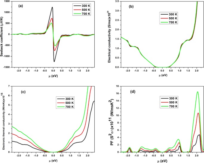
The electronic transport coefficients of BAs sheet with different temperatures have been calculated using the semiclassical Boltzmann theory and constant time approximation. The rigid band model was employed to calculate the thermoelectric coefficients for different chemical potential values. Figure 12 shows the variation of thermoelectric properties like the Seebeck coefficient (S), electrical conductivity (σ), electronic thermal conductivity (ke), and power factor of BAs sheet, with chemical potential (μ) at different temperatures (300, 500, and 700 K). The positive value of chemical potential (μ) represents n-type doping, and negative value indicates p-type doping. The Seebeck coefficient as a function of chemical potential at different temperatures is depicted in Figure 12a. As observed from the figure, the maximum values of the Seebeck coefficient are obtained for the range −0.5–0.5 eV of chemical potential. Beyond this range the curves tends to 0. The highest value of the Seebeck coefficient (−1242.19 μV/K) is obtained at 300 K. The negative value shows that the electrons diffuse from the hot end to the cold end, thereby enhancing concentration of electrons in the cold end with reference to the hot end.58,59 The Seebeck coefficient values decrease with increase in the temperature, due to the augmentation of electron and hole conductivities by enhancement of thermal energy.60 The calculated Seebeck coefficient value is higher than that of MoSe2,61 WSe2,61 graphydiyne,62 phosphorene,63 transition-metal silicides,64 and other conventional thermoelectric materials,65 which implies that BAs sheets can be favorably employed as a thermoelectric material. Overall, this material is an n-type semiconductor combined with good thermoelectric performance. Figure 12b shows the variation of electrical conductivity with chemical potential at different temperatures. The value of electrical conductivity is 0 in the range −0.5–0.5 eV. However, beyond this range, the value of electrical conductivity increases with chemical potential. Further, the changes in the electrical conductivity with chemical potential are similar at different temperatures. The value of electrical conductivity is appreciably high for positive chemical potentials when compared with negative values, implying that n-type carrier is more than p-type composition.
Figure 12.
Calculated (a) Seebeck coefficient, (b) electrical conductivity, (c) electronic thermal conductivity, and (d) power factor with different chemical potentials of a BAs sheet.
Figure 12c depicts the variation of electronic thermal conductivity with μ at various temperatures. These plots show that the enhancement of electronic thermal conductivity takes place with increase in the chemical potential and temperature. It is considerably higher for positive chemical potential with reference to the negative chemical potential, suggesting that enhancement in carrier concentration increases the mobility, which in turn amplifies the electronic thermal conductivity.
The power factor is a key parameter that influences the thermoelectric performance of the material. The changes in the power factor with chemical potential at various temperatures are depicted in Figure 12d. The maximum value of the power factor is obtained as 16.46 × 10¹¹ W/(m s K2) for n-type doping at 700 K. Hence, the calculated Seebeck coefficient and power factor are higher than those of some of the available conventional thermoelectric materials and thus this new material BAs is a promising candidate in the field of thermoelectricity.
Thermodynamic Properties
We have calculated thermodynamic properties such as free energy, entropy, and constant volume heat capacity (Cv) of BAs sheets using the phonon frequency. Figure 13 elicits the changes in the free energy, entropy, and Cv as a function of temperature. It can be noticed from the figure that the heat capacity of BAs is 22.8 J/(K mol) at 300 K. The decrease in free energy with increase in temperature can also be observed. As expected, entropy increases with increase in temperature. The entropy and specific heat values are zero at 0 K, which is in complete agreement with the third law of thermodynamics.
Figure 13.
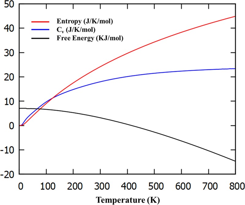
Calculated free energy, entropy, and constant volume specific heat capacity of BAs sheet.
Conclusions
In summary, the first-principle calculations provided valuable insight into electronic, transport, optical, thermoelectric, and thermodynamic properties of BAs sheets. The stability of a two-dimensional sheet is assessed by energetics, phonon distribution, and molecular dynamics simulations. The electronic structure calculations reveal that BAs is a direct band gap semiconductor and the band gap can be tuned by the application of external biaxial strain. The application of biaxial strain (from ε = 0 to 8%) leads to increase in the band gap, and after 8%, the splitting of the conduction band takes place. At a biaxial strain of 10%, the transition from a direct semiconductor nature to indirect band gap nature occurs. With further increase of biaxial strain, the band gap decreases and the material becomes metallic at ε = 14%. Furthermore, both armchair and zigzag nanoribbons of BAs sheets have been designed and their electronic properties have been calculated. Results reveal that both nanoribbons are semiconductor and the band gap values are dependent on the width of the ribbon. The calculated transmission spectra and I–V characteristics highlight that the value of the output current increases with increase in the input bias voltage. To explore the application of this material in the field of optoelectronics, the dielectric function and absorption coefficients have been predicted. Considerable optical anisotropy is observed for parallel and perpendicular polarizations of the electric field, and the material shows strong absorption in the UV and visible regions. The calculated Seebeck coefficient and power factor values elicit the favorable application of BAs sheet in the field of thermoelectric applications. The calculated thermodynamic results highlight that the entropy and constant volume specific heat capacity values increase and free-energy values decrease with increase in the temperature. The comprehensive study of electronic, optical, transport, thermoelectric, and thermodynamic properties of BAs sheets presented in this work is expected to form a solid foundation for the various applications of this 2D material.
Computational Method
The geometrical, electronic, and phonon calculations of BAs sheets were carried out using density functional theory (DFT)-based calculations within projected augmented wave and a plane wave basis, as implemented in Quantum ESPRESSO package.54 The generalized gradient approximation as suggested by Perdew, Burke, and Ernzerhof66 was employed. The plane waves were expanded with a kinetic energy cutoff of 45 Ry. Convergence thresholds of 10–6 Ry and 0.002 Ry/bohr were used for energy and forces, respectively. Periodic boundary conditions were used throughout the study. A vacuum spacing of 12 Å was introduced along a nonperiodic direction to minimize the spurious interactions between periodic supercell images. Monkhorst–Pack67k-point meshes of 8 × 8 × 1 and 16 × 16 × 1 were used for geometrical and electronic structure calculations. The optical and transport properties were calculated using Siesta package.68 The thermoelectric properties were calculated using the semiclassical Boltzmann transport theory and the rigid band approach, as implemented in the BoltzTraP code.69 The constant scattering time approximation was used, which accurately describes the thermoelectric properties of many materials.70,71
Acknowledgments
The authors wish to acknowledge the Science and Engineering Research Board, Department of Science and Technology, New Delhi for funding through the project entitled “Design and Development of Two-Dimensional van der Waals Solids and their Applications” (Project No. EMR/2015/000447) and CSIR-4PI for providing additional computational facility to carry out simulation. K.M. wishes to acknowledge the Council of Scientific and Industrial Research (CSIR), New Delhi for the award of Senior Research Fellowship (SRF).
Supporting Information Available
The Supporting Information is available free of charge on the ACS Publications website at DOI: 10.1021/acsomega.8b00946.
Electronic band structures of 2D sheets of BAs with different biaxial strains and BAs nanoribbons, Wyckoff position of BAs sheet, and IV characteristics of BAs nanoribbons (PDF)
The authors declare no competing financial interest.
Supplementary Material
References
- Geim A. K.; Novoselov K. S. The Rise of Graphene. Nat. Mater. 2007, 6, 183–191. 10.1038/nmat1849. [DOI] [PubMed] [Google Scholar]
- Song L.; Ci L.; Lu H.; Sorokin P. B.; Jin C.; Ni J.; Kvashnin A. G.; Kvashnin D. G.; Lou J.; Yakobson B. I.; et al. Large Scale Growth and Characterization of Atomic Hexagonal Boron Nitride Layers. Nano Lett. 2010, 10, 3209–3215. 10.1021/nl1022139. [DOI] [PubMed] [Google Scholar]
- Wilson J. A.; Yoffe A. D. The Transition Metal Dichalcogenides Discussion and Interpretation of the Observed Optical, Electrical and Structural Properties. Adv. Phys. 1969, 18, 193–335. 10.1080/00018736900101307. [DOI] [Google Scholar]
- Manzeli S.; Ovchinnikov D.; Pasquier D.; Yazyev O. V.; Kis A. 2D Transition Metal Dichalcogenides. Nat. Rev. Mater. 2017, 2, 17033. 10.1038/natrevmats.2017.33. [DOI] [Google Scholar]
- Xu M.; Liang T.; Shi M.; Chen H. Graphene-Like Two-Dimensional Materials. Chem. Rev. 2013, 113, 3766–3798. 10.1021/cr300263a. [DOI] [PubMed] [Google Scholar]
- Miró P.; Audiffred M.; Heine T. An Atlas of Two-Dimensional Materials. Chem. Soc. Rev. 2014, 43, 6537–6554. 10.1039/C4CS00102H. [DOI] [PubMed] [Google Scholar]
- Zhang S.; Yan Z.; Li Y.; Chen Z.; Zeng H. Atomically Thin Arsenene and Antimonene: Semimetal-Semiconductor and Indirect-Direct Band-Gap Transitions. Angew. Chem., Int. Ed. 2015, 54, 3112–3115. 10.1002/anie.201411246. [DOI] [PubMed] [Google Scholar]
- Zhang S.; Zhou W.; Ma Y.; Ji J.; Cai B.; Yang S. A.; Zhu Z.; Chen Z.; Zeng H. Antimonene Oxides: Emerging Tunable Direct Bandgap Semiconductor and Novel Topological Insulator. Nano Lett. 2017, 17, 3434–3440. 10.1021/acs.nanolett.7b00297. [DOI] [PubMed] [Google Scholar]
- Perreault F.; Fonseca de Faria A.; Elimelech M. Environmental Applications of Graphene-Based Nanomaterials. Chem. Soc. Rev. 2015, 44, 5861–5896. 10.1039/C5CS00021A. [DOI] [PubMed] [Google Scholar]
- Zhang S.; Guo S.; Chen Z.; Wang Y.; Gao H.; Gómez-Herrero J.; Ares P.; Zamora F.; Zhu Z.; Zeng H. Recent Progress in 2D Group-VA Semiconductors: From Theory to Experiment. Chem. Soc. Rev. 2018, 47, 982–1021. 10.1039/C7CS00125H. [DOI] [PubMed] [Google Scholar]
- Zhou W.; Guo S.; Zhang S.; Zhu Z.; Song X.; Niu T.; Zhang K.; Liu X.; Zou Y.; Zeng H. DFT Coupled with NEGF Study of a Promising Two-Dimensional Channel Material: Black Phosphorene-Type GaTeCl. Nanoscale 2018, 10, 3350–3355. 10.1039/C7NR08252E. [DOI] [PubMed] [Google Scholar]
- Bhimanapati G. R.; Lin Z.; Meunier V.; Jung Y.; Cha J.; Das S.; Xiao D.; Son Y.; Strano M. S.; Cooper V. R.; et al. Recent Advances in Two-Dimensional Materials beyond Graphene. ACS Nano 2015, 9, 11509–11539. 10.1021/acsnano.5b05556. [DOI] [PubMed] [Google Scholar]
- Lin Y.; Connell J. W. Advances in 2D Boron Nitride Nanostructures: Nanosheets, Nanoribbons, Nanomeshes, and Hybrids with Graphene. Nanoscale 2012, 4, 6908. 10.1039/c2nr32201c. [DOI] [PubMed] [Google Scholar]
- Hinnemann B.; Moses P. G.; Bonde J.; Jørgensen K. P.; Nielsen J. H.; Horch S.; Chorkendorff I.; Nørskov J. K. Biomimetic Hydrogen Evolution: MoS2 Nanoparticles as Catalyst for Hydrogen Evolution. J. Am. Chem. Soc. 2005, 127, 5308–5309. 10.1021/ja0504690. [DOI] [PubMed] [Google Scholar]
- Umadevi D.; Panigrahi S.; Sastry G. N. Noncovalent Interaction of Carbon Nanostructures. Acc. Chem. Res. 2014, 47, 2574–2581. 10.1021/ar500168b. [DOI] [PubMed] [Google Scholar]
- Weng Q.; Wang X.; Wang X.; Bando Y.; Golberg D. Functionalized Hexagonal Boron Nitride Nanomaterials: Emerging Properties and Applications. Chem. Soc. Rev. 2016, 45, 3989–4012. 10.1039/C5CS00869G. [DOI] [PubMed] [Google Scholar]
- Novoselov K. S.; Fal’ko V. I.; Colombo L.; Gellert P. R.; Schwab M. G.; Kim K. A Roadmap for Graphene. Nature 2012, 490, 192–200. 10.1038/nature11458. [DOI] [PubMed] [Google Scholar]
- Bolotin K. I.; Sikes K. J.; Jiang Z.; Klima M.; Fudenberg G.; Hone J.; Kim P.; Stormer H. L. Ultrahigh Electron Mobility in Suspended Graphene. Solid State Commun. 2008, 146, 351–355. 10.1016/j.ssc.2008.02.024. [DOI] [Google Scholar]
- He S.; Song B.; Li D.; Zhu C.; Qi W.; Wen Y.; Wang L.; Song S.; Fang H.; Fan C. A Graphene Nanoprobe for Rapid, Sensitive, and Multicolor Fluorescent DNA Analysis. Adv. Funct. Mater. 2010, 20, 453–459. 10.1002/adfm.200901639. [DOI] [Google Scholar]
- Mudedla S. K.; Balamurugan K.; Kamaraj M.; Subramanian V. Interaction of Nucleobases with Silicon Doped and Defective Silicon Doped Graphene and Optical Properties. Phys. Chem. Chem. Phys. 2016, 18, 295–309. 10.1039/C5CP06059A. [DOI] [PubMed] [Google Scholar]
- Balamurugan K.; Subramanian V. Adsorption of Chlorobenzene onto (5,5) Armchair Single-Walled Carbon Nanotube and Graphene Sheet: Toxicity versus Adsorption Strength. J. Phys. Chem. C 2013, 117, 21217–21227. 10.1021/jp403646h. [DOI] [Google Scholar]
- Kamaraj M.; Sundar J. V.; Subramanian V. Dioxin Sensing Properties of Graphene and Hexagonal Boron Nitride Based van Der Waals Solids: A First-Principles Study. RSC Adv. 2016, 6, 107114–107126. 10.1039/C6RA18976H. [DOI] [Google Scholar]
- Schedin F.; Geim A. K.; Morozov S. V.; Hill E. W.; Blake P.; Katsnelson M. I.; Novoselov K. S. Detection of Individual Gas Molecules Adsorbed on Graphene. Nat. Mater. 2007, 6, 652–655. 10.1038/nmat1967. [DOI] [PubMed] [Google Scholar]
- Varghese S. S.; Lonkar S.; Singh K. K.; Swaminathan S.; Abdala A. Recent Advances in Graphene Based Gas Sensors. Sens. Actuators, B 2015, 218, 160–183. 10.1016/j.snb.2015.04.062. [DOI] [Google Scholar]
- Xia F.; Farmer D. B.; Lin Y. M.; Avouris P. Graphene Field-Effect Transistors with High on/off Current Ratio and Large Transport Band Gap at Room Temperature. Nano Lett. 2010, 10, 715–718. 10.1021/nl9039636. [DOI] [PubMed] [Google Scholar]
- He G.; Ghosh K.; Singisetti U.; Ramamoorthy H.; Somphonsane R.; Bohra G.; Matsunaga M.; Higuchi A.; Aoki N.; Najmaei S.; et al. Conduction Mechanisms in CVD-Grown Monolayer MoS2 Transistors: From Variable-Range Hopping to Velocity Saturation. Nano Lett. 2015, 15, 5052–5058. 10.1021/acs.nanolett.5b01159. [DOI] [PubMed] [Google Scholar]
- Liu H.; Liu Y.; Zhu D. Chemical Doping of Graphene. J. Mater. Chem. 2011, 21, 3335. 10.1039/C0JM02922J. [DOI] [Google Scholar]
- Zhang Z.; Huang H.; Yang X.; Zang L. Tailoring Electronic Properties of Graphene by π–π Stacking with Aromatic Molecules. J. Phys. Chem. Lett. 2011, 2, 2897–2905. 10.1021/jz201273r. [DOI] [Google Scholar]
- Şahin H.; Cahangirov S.; Topsakal M.; Bekaroglu E.; Akturk E.; Senger R. T.; Ciraci S. Monolayer Honeycomb Structures of Group-IV Elements and III-V Binary Compounds: First-Principles Calculations. Phys. Rev. B 2009, 80, 155453. 10.1103/PhysRevB.80.155453. [DOI] [Google Scholar]
- Mannix A. J.; Zhou X.-F.; Kiraly B.; Wood J. D.; Alducin D.; Myers B. D.; Liu X.; Fisher B. L.; Santiago U.; Guest J. R.; et al. Synthesis of Borophenes: Anisotropic, Two-Dimensional Boron Polymorphs. Science 2015, 350, 1513–1516. 10.1126/science.aad1080. [DOI] [PMC free article] [PubMed] [Google Scholar]
- Zhao J.; Liu H.; Yu Z.; Quhe R.; Zhou S.; Wang Y.; Liu C. C.; Zhong H.; Han N.; Lu J.; et al. Rise of Silicene: A Competitive 2D Material. Prog. Mater. Sci. 2016, 83, 24–151. 10.1016/j.pmatsci.2016.04.001. [DOI] [Google Scholar]
- Tao L.; Cinquanta E.; Chiappe D.; Grazianetti C.; Fanciulli M.; Dubey M.; Molle A.; Akinwande D. Silicene Field-Effect Transistors Operating at Room Temperature. Nat. Nanotechnol. 2015, 10, 227–231. 10.1038/nnano.2014.325. [DOI] [PubMed] [Google Scholar]
- Xiao H.; Cao W.; Ouyang T.; Guo S.; He C.; Zhong J. Lattice Thermal Conductivity of Borophene from First Principle Calculation. Sci. Rep. 2017, 7, 45986. 10.1038/srep45986. [DOI] [PMC free article] [PubMed] [Google Scholar]
- Williams F. V.; Ruehrwein R. A. The Preparation and Properties of Boron Phosphides and Arsenides. J. Am. Chem. Soc. 1960, 82, 1330–1332. 10.1021/ja01491a014. [DOI] [Google Scholar]
- Wang S.; Swingle S. F.; Ye H.; Fan F. R. F.; Cowley A. H.; Bard A. J. Synthesis and Characterization of a P-Type Boron Arsenide Photoelectrode. J. Am. Chem. Soc. 2012, 134, 11056–11059. 10.1021/ja301765v. [DOI] [PubMed] [Google Scholar]
- Lindsay L.; Broido D. A.; Reinecke T. L. First-Principles Determination of Ultrahigh Thermal Conductivity of Boron Arsenide: A Competitor for Diamond?. Phys. Rev. Lett. 2013, 111, 025901. 10.1103/PhysRevLett.111.025901. [DOI] [PubMed] [Google Scholar]
- Boudjemline A.; Islam M. M.; Louail L.; Diawara B. Electronic and Optical Properties of BAs under Pressure. Phys. B 2011, 406, 4272–4277. 10.1016/j.physb.2011.08.043. [DOI] [Google Scholar]
- Osugi J.; Shimizu K.; Tanaka Y.; Kadono K. Preparation and Chemical Properties of Cubic Boron Arsenide, BAs. Rev. Phys. Chem. Jpn. 1966, 36, 54–57. [Google Scholar]
- Hart G. L. W.; Zunger A. Electronic Structure of BAs and Boride III-V Alloys. Phys. Rev. B: Condens. Matter Mater. Phys. 2000, 62, 13522–13537. 10.1103/PhysRevB.62.13522. [DOI] [Google Scholar]
- Tong C.-J.; Zhang H.; Zhang Y.-N.; Liu H.; Liu L.-M. New Manifold Two-Dimensional Single-Layer Structures of Zinc-Blende Compounds. J. Mater. Chem. A 2014, 2, 17971–17978. 10.1039/C4TA03944K. [DOI] [Google Scholar]
- Zhuang H. L.; Hennig R. G. Electronic Structures of Single-Layer Boron Pnictides. Appl. Phys. Lett. 2012, 101, 153109. 10.1063/1.4758465. [DOI] [Google Scholar]
- Silvi B.; Savin A. Classification of Chemical Bonds Based on Topological Analysis of Electron Localization Functions. Nature 1994, 371, 683–686. 10.1038/371683a0. [DOI] [Google Scholar]
- Kamal C.; Ezawa M. Arsenene: Two-Dimensional Buckled and Puckered Honeycomb Arsenic Systems. Phys. Rev. B 2015, 91, 085423. 10.1103/PhysRevB.91.085423. [DOI] [Google Scholar]
- Liu M.-Y.; Huang Y.; Chen Q.-Y.; Cao C.; He Y. Unexpected Electronic Structure of the Alloyed and Doped Arsenene Sheets: First-Principles Calculations. Sci. Rep. 2016, 6, 29114. 10.1038/srep29114. [DOI] [PMC free article] [PubMed] [Google Scholar]
- Garg P.; Kumar S.; Choudhuri I.; Mahata A.; Pathak B. Hexagonal Planar CdS Monolayer Sheet for Visible Light Photocatalysis. J. Phys. Chem. C 2016, 120, 7052–7060. 10.1021/acs.jpcc.6b01622. [DOI] [Google Scholar]
- Ji Y.; Yang M.; Dong H.; Wang L.; Hou T.; Li Y. Monolayer Group IVA Monochalcogenides as Potential and Efficient Catalysts for the Oxygen Reduction Reaction from First-Principles Calculations. J. Mater. Chem. A 2017, 5, 1734–1741. 10.1039/C6TA08321H. [DOI] [Google Scholar]
- Yang L. M.; Ganz E. Adding a New Dimension to the Chemistry of Phosphorus and Arsenic. Phys. Chem. Chem. Phys. 2016, 18, 17586–17591. 10.1039/C6CP01860B. [DOI] [PubMed] [Google Scholar]
- Ding Y.; Wang Y. Density Functional Theory Study of the Silicene-like SiX and XSi3 (X = B, C, N, Al, P) Honeycomb Lattices: The Various Buckled Structures and Versatile Electronic Properties. J. Phys. Chem. C 2013, 117, 18266–18278. 10.1021/jp407666m. [DOI] [Google Scholar]
- Cahangirov S.; Topsakal M.; Aktürk E.; Sahin H.; Ciraci S. Two- and One-Dimensional Honeycomb Structures of Silicon and Germanium. Phys. Rev. Lett. 2009, 102, 236804. 10.1103/PhysRevLett.102.236804. [DOI] [PubMed] [Google Scholar]
- Qiao M.; Wang Y.; Li Y.; Chen Z. Tetra-Silicene: A Semiconducting Allotrope of Silicene with Negative Poisson’s Ratios. J. Phys. Chem. C 2017, 121, 9627–9633. 10.1021/acs.jpcc.7b02413. [DOI] [Google Scholar]
- Molina-Sánchez A.; Wirtz L. Phonons in Single-Layer and Few-Layer MoS2 and WS2. Phys. Rev. B 2011, 84, 155413. 10.1103/PhysRevB.84.155413. [DOI] [Google Scholar]
- Qin G.; Yan Q.-B.; Qin Z.; Yue S.-Y.; Hu M.; Su G. Anisotropic Intrinsic Lattice Thermal Conductivity of Phosphorene from First Principles. Phys. Chem. Chem. Phys. 2015, 17, 4854–4858. 10.1039/C4CP04858J. [DOI] [PubMed] [Google Scholar]
- Clark S. J.; Segall M. D.; Pickard C. J.; Hasnip P. J.; Probert M. I. J.; Refson K.; Payne M. C. First Principles Methods Using CASTEP. Z. Kristallogr. - Cryst. Mater. 2005, 220, 567–570. 10.1524/zkri.220.5.567.65075. [DOI] [Google Scholar]
- Giannozzi P.; Baroni S.; Bonini N.; Calandra M.; Car R.; Cavazzoni C.; Ceresoli D.; Chiarotti G. L.; Cococcioni M.; Dabo I. QUANTUM ESPRESSO: A Modular and Open-Source Software Project for Quantum Simulations of Materials. J. Phys.: Condens. Matter 2009, 21, 395502. 10.1088/0953-8984/21/39/395502. [DOI] [PubMed] [Google Scholar]
- Born M.; Huang K.; Lax M. Dynamical Theory of Crystal Lattices. Am. J. Phys. 1955, 23, 474. 10.1119/1.1934059. [DOI] [Google Scholar]
- Dávila M. E.; Lew Yan Voon L. C.; Zhao J.; Le Lay G. Elemental Group IV Two-Dimensional Materials Beyond Graphene. Semicond. Semimetals 2016, 149–188. 10.1016/bs.semsem.2016.04.003. [DOI] [Google Scholar]
- Brandbyge M.; Mozos J.-L.; Ordejón P.; Taylor J.; Stokbro K. Density-Functional Method for Nonequilibrium Electron Transport. Phys. Rev. B 2002, 65, 165401. 10.1103/PhysRevB.65.165401. [DOI] [Google Scholar]
- Seitz F.; Johnson R. P. Modern Theory of Solids. I. J. Appl. Phys. 1937, 8, 84–97. 10.1063/1.1710273. [DOI] [Google Scholar]
- Seitz F.; Johnson R. P. Modern Theory of Solids. II. J. Appl. Phys. 1937, 8, 186–199. 10.1063/1.1710281. [DOI] [Google Scholar]
- Lee C.; Hong J.; Lee W. R.; Kim D. Y.; Shim J. H. Density Functional Theory Investigation of the Electronic Structure and Thermoelectric Properties of Layered MoS2, MoSe2 and Their Mixed-Layer Compound. J. Solid State Chem. 2014, 211, 113–119. 10.1016/j.jssc.2013.12.012. [DOI] [Google Scholar]
- Kumar S.; Schwingenschlögl U. Thermoelectric Response of Bulk and Monolayer MoSe2 and WSe2. Chem. Mater. 2015, 27, 1278–1284. 10.1021/cm504244b. [DOI] [Google Scholar]
- Sun L.; Jiang P. H.; Liu H. J.; Fan D. D.; Liang J. H.; Wei J.; Cheng L.; Zhang J.; Shi J. Graphdiyne: A Two-Dimensional Thermoelectric Material with High Figure of Merit. Carbon 2015, 90, 255–259. 10.1016/j.carbon.2015.04.037. [DOI] [Google Scholar]
- Lv H. Y.; Lu W. J.; Shao D. F.; Sun Y. P.. Large Thermoelectric Power Factors in Black Phosphorus and Phosphorene, arXiv:1404.5171. https://arxiv.org/abs/1404.5171 (submitted Apr 21, 2014).
- Opahle I.; Parma A.; McEniry E. J.; Drautz R.; Madsen G. K. H. High-Throughput Study of the Structural Stability and Thermoelectric Properties of Transition Metal Silicides. New J. Phys. 2013, 15, 105010. 10.1088/1367-2630/15/10/105010. [DOI] [Google Scholar]
- Pei Y.; LaLonde A.; Iwanaga S.; Snyder G. J. High Thermoelectric Figure of Merit in Heavy Hole Dominated PbTe. Energy Environ. Sci. 2011, 4, 2085. 10.1039/c0ee00456a. [DOI] [Google Scholar]
- Perdew J. P.; Burke K.; Ernzerhof M. Generalized Gradient Approximation Made Simple. Phys. Rev. Lett. 1996, 77, 3865–3868. 10.1103/PhysRevLett.77.3865. [DOI] [PubMed] [Google Scholar]
- Monkhorst H. J.; Pack J. D. Special Points for Brillouin-Zone Integrations. Phys. Rev. B 1976, 13, 5188–5192. 10.1103/PhysRevB.13.5188. [DOI] [Google Scholar]
- Soler J. M.; Artacho E.; Gale J. D.; García A.; Junquera J.; Ordejón P.; Sánchez-Portal D. The SIESTA Method for Ab Initio Order- N Materials Simulation. J. Phys.: Condens. Matter 2002, 14, 2745–2779. 10.1088/0953-8984/14/11/302. [DOI] [Google Scholar]
- Madsen G. K. H.; Singh D. J. BoltzTraP. A Code for Calculating Band-Structure Dependent Quantities. Comput. Phys. Commun. 2006, 175, 67–71. 10.1016/j.cpc.2006.03.007. [DOI] [Google Scholar]
- Vo T. T. M.; Williamson A. J.; Lordi V.; Galli G. Atomistic Design of Thermoelectric Properties of Silicon Nanowires. Nano Lett. 2008, 8, 1111–1114. 10.1021/nl073231d. [DOI] [PubMed] [Google Scholar]
- Kaur K.; Kumar R. First Principle Investigation of the Electronic and Thermoelectric Properties of Mg2C. Chin. Phys. B 2016, 25, 026402. 10.1088/1674-1056/25/2/026402. [DOI] [Google Scholar]
Associated Data
This section collects any data citations, data availability statements, or supplementary materials included in this article.


