Abstract

The self-heating effect is a severe issue for high-power semiconductor devices, which degrades the electron mobility and saturation velocity, and also affects the device reliability. On applying an ultrafast and high-resolution thermoreflectance imaging technique, the direct self-heating effect and surface temperature increase phenomenon are observed on novel top-gate β-Ga2O3 on insulator field-effect transistors. Here, we demonstrate that by utilizing a higher thermal conductivity sapphire substrate rather than a SiO2/Si substrate, the temperature rise above room temperature of β-Ga2O3 on the insulator field-effect transistor can be reduced by a factor of 3 and thereby the self-heating effect is significantly reduced. Both thermoreflectance characterization and simulation verify that the thermal resistance on the sapphire substrate is less than 1/3 of that on the SiO2/Si substrate. Therefore, maximum drain current density of 535 mA/mm is achieved on the sapphire substrate, which is 70% higher than that on the SiO2/Si substrate due to reduced self-heating. Integration of β-Ga2O3 channel on a higher thermal conductivity substrate opens a new route to address the low thermal conductivity issue of β-Ga2O3 for power electronics applications.
Introduction
The self-heating effect (SHE)-induced temperature increase and nonuniform distribution of dissipated power have emerged as one of the most important concerns in the degradation of transistor’s drain current (ID), output power density (P), as well as the gate leakage current, device variability, and reliability.1−5 This effect would become more severe in a high-power device with a low thermal conductivity (κ) substrate such as β-Ga2O3. β-Ga2O3 as a newly emerged semiconductor has an ultrawide band gap of 4.8 eV and a corresponding high electrical breakdown field (Ebr) of 8 MV/cm, being identified as the next generation wide band gap semiconductor to replace GaN and SiC.6−9 In addition, the transferrable nanomembrane property could also offer more functionalities for β-Ga2O3 by transferring on different substrates.7 However, the β-Ga2O3 bulk substrate generally suffers from low κ of 10–25 W/(m·K) and thus severe SHE,10,11 which becomes one of the major challenges for realizing practical applications. An effective approach to mitigate the SHE of β-Ga2O3 field-effect transistors (FETs) is to utilize a higher κ substrate rather than the β-Ga2O3 native substrate through a potential wafer bonding technique. In our previous work, we have demonstrated high-performance back-gate β-Ga2O3 on insulator (GOOI) FETs by transferring β-Ga2O3 nanomembranes or nanobelts to a SiO2/Si substrate with 300 nm SiO2 as the gate voltage blocking layer and a Si substrate as the thermal conductor.12,13 A unique property of β-Ga2O3 is its large lattice constant of 12.23 Å along [100] direction, which allows a facile cleavage into the nanomembrane along this [100] direction. Therefore, thin-film β-Ga2O3 nanomembrane can be obtained by applying mechanical exfoliation, although β-Ga2O3 is not a van der Waals two-dimensional (2D) material.12
Nowadays, a majority of the GOOI FETs were fabricated on the SiO2/Si substrate like most of the 2D devices, such as graphene,14 MoS2,15 and black phosphorus;16 however, SiO2 has a low room temperature κ of 1.5 W/(m·K). To reduce the SHE of GOOI FET, a higher κ substrate is needed. Although SiC has a high κ of 300 W/(m·K), it is not an ideal substrate for β-Ga2O3 because of its lower band gap of 3.3 eV and high cost.17 Diamond is a promising substrate for β-Ga2O3 with higher thermal conductivity, once its low-cost large-sized substrates are available.6 Among these commercial, large-sized, and wide band gap substrates, sapphire stands out to be a promising candidate for GOOI FETs, because of its low-cost, wide band gap of 8.8 eV, and medium κ of 40 W/(m·K),18 which is around 2–4 times of the bulk β-Ga2O3 substrate and around 25 times of SiO2. In this letter, we have used the sapphire substrate as a thermal conductor for GOOI FETs to enhance the thermal dissipation and boost the electrical device performance significantly. An ultrafast, high-resolution thermoreflectance (TR) imaging technique is applied to the top-gate GOOI FET to examine the reduced SHE and local surface temperature increase (ΔT) above room temperature on a sapphire substrate compared to that in a SiO2/Si substrate. After replacing the SiO2/Si substrate with a sapphire substrate, the top-gate GOOI FET has 70% higher maximum ID (IDmax), ∼ twice lower device surface ΔT, and twice lower thermal resistance (RT).
Results and Discussion
β-Ga2O3 Materials and GOOI FETs
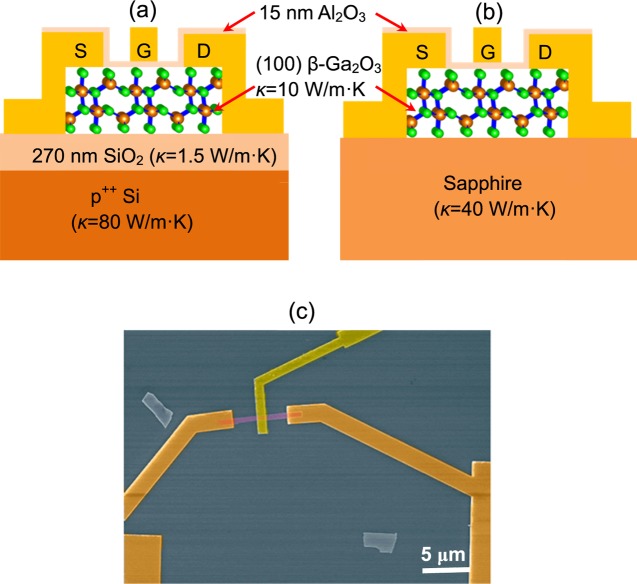
The experimental device cross-sectional schematic of top-gate GOOI FETs on SiO2/Si and sapphire substrates is shown in Figure 1a,b, consisting of a Ni/Au (30/50 nm) top-gate, 15 nm amorphous aluminum oxide (Al2O3) gate dielectric, 70–100 nm Sn-doped (100) β-Ga2O3 channel with surface roughness of 0.3 nm,19 and Ti/Al/Au (15/60/50 nm) source/drain contacts. A 270 nm thick SiO2 is used as the drain voltage blocking layer for top-gate GOOI FETs, and p++ Si is used as a thermal conductor for GOOI FET. The thickness of the c-plane sapphire substrate is 650 μm, which serves as the drain voltage blocking layer and thermal conductor due to its wider band gap and higher κ compared to those of the (100) β-Ga2O3 channel. The κ of each material is also marked in Figure 1a,b for comparison. Figure 1c is the false-colored scanning electron microscopy (SEM) image of a fabricated GOOI FET. The device has a gate length (LG) of 1 μm and source to drain spacing (LSD) of 6 μm to allow high drain bias to generate enough heat for our TR study. This TR imaging technique offers large-area imaging capability with higher spatial resolution (submicron) compared to that of other optical thermal characterization approaches, such as infrared (IR) thermography and micro-Raman. The TR system also enables a high-resolution transient temporal imaging to study the heating/cooling phase at submicrosecond time scales.20,21
Figure 1.
Schematic and fabrication of top-gate GOOI FETs. Cross-sectional schematic view of a top-gate GOOI FET on (a) SiO2/Si and (b) sapphire substrates with different thermal conductivities (κ) marked. Al2O3 (15 nm) is used as the gate dielectric, Ti/Al/Au (15/60/50 nm) is used as the source and drain electrode, and Ni/Au (30/50 nm) is used as the gate electrode. (c) False-colored SEM top view of a GOOI FET, with LG = 1 μm and LSD = 6 μm.
I–V Electrical Characteristics
Figure 2a,b shows the well-behaved direct-current (DC) output characteristics (ID–VDS) of two top-gate GOOI FETs with LSD of 6/6.5 μm, LG of 1 μm, and channel thickness of 73/75 nm on SiO2/Si and sapphire substrates, respectively. The typical range of physical width of nanomembrane devices is 0.5–1.5 μm, determined by SEM, as shown in Figure 1c. The measurements start from applying the top-gate bias (VGS) to 8 or 6 V and then stepping to the device pinch-off voltage of −28 V with −2 V as a step, whereas the drain bias (VDS) is swept from 0 to 27 or 30 V for the SiO2/Si and sapphire substrate devices, respectively. IDmax of 535 and 325 mA/mm for sapphire and SiO2/Si substrates are obtained, respectively; the IDmax on sapphire is the highest among all DC values of all top-gate β-Ga2O3 MOSFETs.6−9,22,23 The IDmax of GOOI FET on the sapphire substrate is around 1.7 times that on the SiO2/Si substrate, originating from better transport properties at a lower device temperature. Figure 2c depicts the ID–VGS and gm–VGS of GOOI FETs on two substrates at VDS = 25 V. A similar on/off ratio of 109 and low subthreshold slope (SS) of 65 mV/dec are achieved on both devices due to the wide band gap and high-quality atomic-layer-deposition (ALD) Al2O3/β-Ga2O3 interface, yielding a low interface trap density (Dit) of 2.6 × 10¹¹/eV·cm2 by the equation SS = 60 × (1 + qDit/Cox) mV/dec at room temperature, where Cox is the oxide capacitance. The slightly high off-state current is due to the limitation of the lowest current level the equipment setup can measure on small width devices. One interesting phenomenon is that the peak gm of the sapphire substrate is 21 mS/mm, which is 60% higher than the gm of the SiO2/Si substrate. The extrinsic electron field-effect mobility (μFE) of GOOI FET on sapphire and SiO2/Si are roughly extracted to be 30.2 and 21.7 cm2/(V·s), respectively, benefiting from the less SHE on sapphire.24 More than 10 devices on 2 different substrates were fabricated and characterized. Their mobilities were extracted with small standard deviations, which confirms that the mobility on the sapphire substrate is higher and the fabricated devices have high uniformity.
Figure 2.
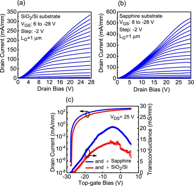
I–V electrical characteristics of top-gate GOOI FETs. ID–VDS output characteristics of GOOI FETs on (a) the SiO2/Si substrate and (b) sapphire substrate, with LSD = 6–6.5 μm and LG = 1 μm. A record high IDmax = 535 mA/mm is demonstrated on top-gate β-Ga2O3 GOOI FETs. (c) ID–gm–VDS transfer characteristics of GOOI FETs on both substrates with a high on/off ratio of 109 and low SS of 65 mV/dec, yielding a low Dit of 2.6 × 10¹¹/eV·cm2. Higher gm shows higher electron μ on the sapphire substrate due to the reduced device temperature.
Steady State TR Imaging
For power electronics applications with large ID and VDS, the SHE must be taken into consideration. The power consumption (P) of the active device can be simply estimated as a product of ID and VDS; then, the heat generated in an active device is proportional to the device power consumption. In a GOOI FET, the device serves as the heat source and substrate acts as the heat sink for dissipation of the device heat. Heat can also be dissipated through the top surface by air convection and source–gate–drain metal pads.4 However, the heat transfer to the air is very low, considering the low heat transfer coefficient h ∼ 10 W/(m2·K). A heat flux (F) of 4.6 × 10⁻¹⁰ W can be roughly estimated by equation F = hAΔT, where A is the nanomembrane area of 1 μm × 11 μm and ΔT (43 K) is the device temperature rise above room temperature while being biased for TR measurement. This heat flux is negligible compared with the device power consumption of P = ID × VDS = 30 V × 540 mA/mm × 1 μm = 1.62 × 10⁻² W, which is mainly dissipated through the substrate. During the TR characterization, the gate electrode metal Au is illuminated through a light-emitting diode (LED) and the reflected signal is calibrated with Au TR coefficient to translate into the increased temperature ΔT above room temperature. The gate Au electrode rather than source/drain contacts is selected because source/drain contact regions have Al2O3 on top and the Ti/Al/Au are alloyed. Au directly above the channel region defines the channel temperature, and the Au temperature is marked as the channel temperature.
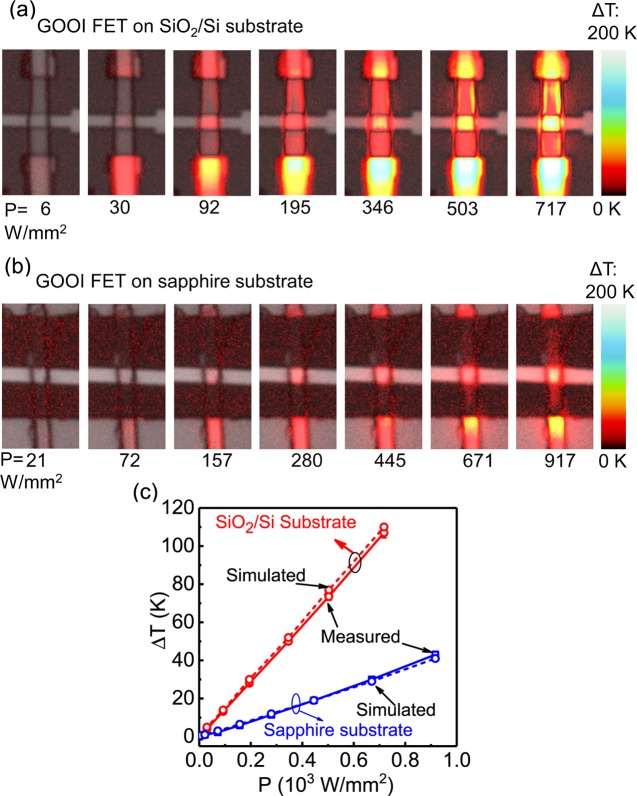
Figure 3a,b shows merged optical and TR thermal image views of GOOI FETs on SiO2/Si and sapphire substrates at steady state and different P conditions. The β-Ga2O3 nanomembrane has a thickness of 100 and 80 nm on SiO2/Si and sapphire substrates, respectively. The 20 nm nanomembrane difference in thickness only contributes to a negligible thermal resistance of 2 × 10⁻⁶ mm2·K/W, which is less than 0.1% of the total resistance. In this measurement, VGS is biased at 0 V, whereas VDS is swept from 0 to 27 V or 30 V for GOOI FETs on SiO2/Si and sapphire, respectively. During the TR measurement, the VDS modulation signal has a pulse width of 1 ms and 10% duty cycle. The 1 ms pulse is long enough to allow the FET to reach the hot steady state during the high portion of the signal. The probe optical pulse width was 100 μs, synchronized just prior to the falling edge of the device excitation pulse to capture the TR image at the end of the VDS pulse. The ID is recorded at the same time to calculate the normalized power density P = VDS × ID/A to avoid different heat dissipation areas from having different sizes of the β-Ga2O3 nanomembrane. The areas of β-Ga2O3 nanomembranes are 1.4 × 10⁻⁵ and 1.1 × 10⁻⁵ mm2 on SiO2/Si and sapphire, respectively. As higher VDS is applied, the device is heated up simultaneously and the corresponding ΔT is increased. At P = 717 W/mm2 on the SiO2/Si substrate, the ΔT is measured to be 106 K, whereas in contrast the ΔT is just 43 K at a higher P = 917 W/mm2 on the sapphire substrate. Figure 3c depicts the measured and simulated ΔT versus P for GOOI FETs on two substrates. For both the measurement and simulation results, the clear observation is that at the same P, the GOOI FET on the sapphire substrate has more than twice lower ΔT compared to that on SiO2/Si. The RT of sapphire and SiO2/Si substrates are calculated to be 4.62 × 10⁻² and 1.47 × 10⁻¹ mm2·K/W, respectively, through RT = ΔT/P. The reduced RT of GOOI FET on sapphire demonstrates that a higher κ substrate can be more effective in dissipating the heat on the devices. With less heat on the device, the temperature is lower so that the μ is higher to achieve a potentially higher IDmax for a better device performance. This substrate thermal engineering approach can also be applied to other 2D FET research if heat dissipation is an issue.
Figure 3.
Steady state TR characteristics and temperature rise of top-gate GOOI FETs. TR and charge-coupled device (CCD) camera merged images of GOOI FET on (a) SiO2/Si and (b) sapphire substrates when device P is increased by increasing VDS at VGS = 0 V. Results show the device heating at steady state, and significant SHE is observed on GOOI FET on the SiO2/Si substrate at high P. (c) Measured and simulated local gate Au surface ΔT comparison between GOOI FET on sapphire and SiO2/Si substrates. Each error bar of measured data is from the standard deviation of three devices on both substrates. The power density P = VDS × ID is normalized by the β-Ga2O3 nanomembrane area to avoid random shape-induced variations. The ΔT of GOOI FET on the SiO2/Si substrate is more than three times of that on the sapphire substrate at the same P. As a result, the RT of GOOI FET on the sapphire substrate is 4.62 × 10⁻² mm2·K/W, which is less than 1/3 of that on the SiO2/Si substrate.
Transient TR Imaging
Although there are well-established methods to access the DC temperature of devices, there is as yet little direct experimental information available on the device dynamics. Such time-dependent information is particularly relevant for this new device system β-Ga2O3. Understanding of heat dissipation and thermal dynamics of the GOOI FETs is furthermore important because pulse width modulation is commonly used to suppress self-heating and improve efficiency in modern power applications. Dynamic measurements help to reveal the surface temperature redistribution and allow the device thermal time constant for both heating (τH) and cooling (τC) to be measured experimentally. Measured thermal time constants can be used to approximate device transient thermal resistance on the basis of a simplified one-dimensional (1D) thermal equivalent circuit model.4 To precisely determine the thermal time constant, the probe optical pulse width is reduced from 100 μs to 50 ns and the VDS pulse width is reduced to 1 μs. The first 1 μs heat up phase corresponds to the state when VDS pulse is on, and the rest 1 μs cool down phase represents the state when VDS pulse is set to be 0 V. Because the thermal time constants are independent of the amplitude of heating, VDS was chosen to produce similar transient heating amplitude for the GOOI FETs on the two different substrates to avoid different temperature-induced variations. Figure 4a,b describes the three-dimensional (3D) plot ΔT of the GOOI FETs on SiO2/Si and sapphire substrates during the heating and cooling dynamics. Figure 4c is the heating and cooling phase comparison between two substrates. It takes GOOI FETs τH of 350 and 350 ns to reach the steady state during the heat up phase and τC of 250 and 300 ns to cool down on SiO2/Si and sapphire substrates. The cooling phase is of particular importance to investigate the heat dissipation through the substrate. Here, we take GOOI FET on the sapphire substrate as an example. The time constant of heat dissipation or cooling phase τC through a material is t2/(κ/ρCV)4, where t is the heat dissipation depth, ρ is the mass density, and CV is the specific heat. Those parameters are listed in Supporting Information. For sapphire substrate, the t is calculated to be 2.03 μm at τC = 300 ns, which yields an overall transient RT of 5.0 × 10⁻² mm2·K/W by RT = t/κ.25 The extracted RT from transient is in good agreement with the steady state RT of 4.62 × 10⁻² mm2·K/W. As for the SiO2/Si substrate, this simplification overestimates transient RT because part of the heat can diffuse up to the gate metal and then get dissipated through lateral diffusion due to the extremely low κ of SiO2.
Figure 4.
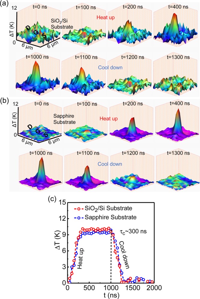
Transient TR characteristics of top-gate GOOI FETs. (a, b) Three-dimensional TR images of heat up and cool down transient phases of GOOI FETs at the gate region on SiO2/Si and sapphire substrates, respectively. (c) Gate region ΔT transient comparison between two devices. GOOI FET on sapphire has a cooling phase τC of 300 ns, yielding an overall transient RT of 5.0 × 10⁻² mm2·K/W, which is in good agreement with steady state TR measurement.
Simulation Verification
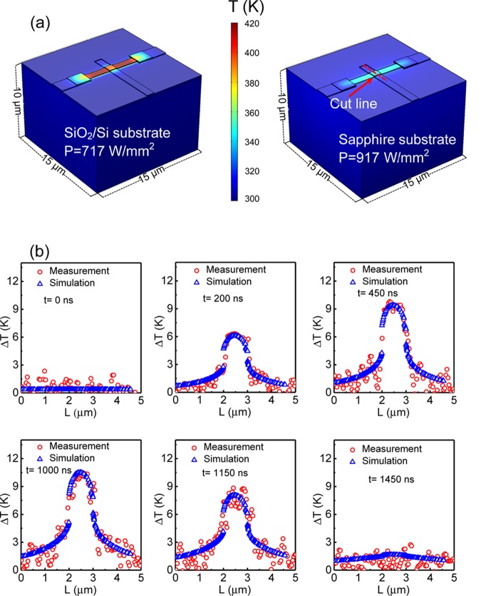
To rationalize our experimental results and evaluate the improvement in the thermal management of GOOI FETs using the sapphire substrate to replace the SiO2/Si substrate, we have also carried out the modeling work to investigate the SHE on the devices with the finite-element method (FEM). In the model, we have defined the heat source as the 80/100 nm thick β-Ga2O3 nanomembranes. The substrate thickness is set to be 10 μm, and the bottom of the substrate is set to be T = 300 K. The thermal boundary resistance (RTB) for β-Ga2O3 systems is not well known; consequently, we use RTB as a fitting parameter in our model. For an initial value of RTB, we use GaN RTB of 1.67 × 10⁻² mm2·K/W between β-Ga2O3 and two substrates. The choice of GaN RTB for the initial value is arbitrary, on the basis of only the prevalence of GaN in power electronics applications.26Figure 5a shows the simulated T distribution of GOOI FET on SiO2/Si and sapphire substrates at P of 717 and 917 W/mm2, corresponding to the respective power applied for the experimental TR images. For GOOI FET on the SiO2/Si substrate, β-Ga2O3 nanomembrane has ΔT = 106 K at the gate region, in great contrast to the ΔT of 41 K on the sapphire substrate, showing the significantly reduced device temperature after implementing a higher κ substrate. Figure 5b shows the transient TR measured ΔT distribution and corresponding FEM simulation of the temperature distribution along the gate width across the channel direction on the sapphire substrate. At all time regimes, both the simulated and measured temperature profiles coincide very well and indicate that the peak temperature is located at the center of the gate region with β-Ga2O3 nanomembrane underneath. This profile possesses a sharp decrease of the temperature at the front and back edges of the β-Ga2O3 nanomembrane, which is normalized to the current conduction direction. This in return verifies our 1D approximation is reasonable in that most of the heat is directly dissipated through the substrate rather than being laterally dissipated through the gate metal. On the contrary, for the GOOI FET on the SiO2/Si substrate, there is a significant amount of heat diffused to gate metal and then laterally dissipated through the gate metal region without the nanomembrane underneath, as indicated in Figure 5a. Therefore, the 1D simplified model has its limitation for application on the SiO2/Si substrate or other low κ substrates. Finally, good agreements are achieved both on the steady state and transient heating and cooling phases, validating our experiments and the TR characterization technique and further confirming the reduced SHE using sapphire as a substrate.
Figure 5.
Simulated temperature distribution in GOOI FETs and experimental design verification. (a) Simulated temperature distribution of GOOI FETs on SiO2/Si and sapphire substrates with device power density of 717 and 917 W/mm2, respectively. GOOI FET on SiO2/Si has more than twice higher ΔT than that of the sapphire substrate, showing the much severe SHE on the SiO2/Si substrate. (b) Simulated and measured temperature distribution along the gate width cutline direction on the sapphire substrate at various heat up and cool down phases. Good agreements are achieved both at steady state and transient time domain between measured and simulated data, verifying our experiment design and characterization.
Conclusions
In summary, we have demonstrated that the sapphire substrate can provide much better thermal dissipation and less SHE than the SiO2/Si substrate for high-power device GOOI FETs. Both the simulation and TR imaging reveal that the GOOI FET on the sapphire substrate has twice lower ΔT compared to that on the SiO2/Si substrate for identical device power density. The RT is extracted and calculated to be 4.6 × 10⁻² and 1.47 × 10⁻¹ mm2·K/W for sapphire and SiO2/Si substrates, respectively. Benefiting from the enhanced heat dissipation, better electronic device performance of GOOI FET on the sapphire substrate is achieved.
Experimental Methods
Device Fabrication
The Sn-doped (2̅01) β-Ga2O3 bulk substrate was purchased from Tamura Corporation, which has a carrier concentration of 2.8 × 1018 cm–3 determined by capacitance–voltage (C–V) measurement. The nanomembranes were mechanically exfoliated from the bulk substrate’s edge cleavage through the scotch tape method. The exfoliation process was repeated to get thin nanomembranes. After the exfoliation, nanomembranes were transferred to the SiO2/Si and sapphire substrates, the same method to get other 2D flakes. Prior to the transfer, the SiO2/p++ Si and sapphire substrates were cleaned in acetone for 24 h and the β-Ga2O3 nanomembrane transfer time was within 1 min. ZEP 520A was used as the electron-beam lithography (EBL) resist in our experiment. Source and drain regions were defined by the VB6 EBL system followed by resist development, Ti/Al/Au metallization and lift-off processes. Thirty seconds of Ar plasma bombardment with radio frequency power of 100 W was adopted to the source and drain regions before metallization to improve the contact formation. The device without Ar bombardment shows more severe Schottky-like behaviors and larger contact resistance. Fifteen nanometers of Al2O3 was then deposited by an ASM F-120 atomic-layer-deposition (ALD) system at 250 °C with trimethyl-aluminum and H2O as precursors. Finally, Ni/Au were deposited as the gate electrode, followed by a lift-off process.
Device Characterization
The thickness and surface roughness of the (100) β-Ga2O3 channel was measured by a Veeco Dimension 3100 AFM system. The C–V measurement was done with an Agilent E4980A LCR meter. The device electric characterizations were carried out by a Keithley 4200 Semiconductor Parameter Analyzer. A Microsanj TR system with high-speed pulsed light-emitting diode (LED) (λ = 530 nm) probe illumination and a synchronized CCD camera were used for the TR measurement equipment.
Acknowledgments
The authors would like to thank Dr. SangHoon Shin for the thermal simulation support and technical guidance from the Sensors Directorate of Air Force Research Laboratory. The work is supported in part by AFOSR (under Grant FA9550-12-1-0180), ONR NEPTUNE (under Grant N00014-15-1-2833), and DTRA (under Grant HDTRA1-12-1-0025).
Supporting Information Available
The Supporting Information is available free of charge on the ACS Publications website at DOI: 10.1021/acsomega.7b01313.
Details about TR measurement setup and timing principles, TR coefficient calibration, photography of the TR measurement equipment, simulation mesh build up, heat pulse generation function for transient measurement, simplified 1D equivalent thermal circuit model, and lists of major materials parameters used for thermal simulation and calculation (PDF)
Author Contributions
P.D.Y. conceived the idea and supervised the experiments. H.Z. performed the device fabrication and material and electrical characterization. H.Z. and J.N. performed the thermal simulation. A.S. supervised H.Z. and K.M. to perform the TR characterization. H.Z. and P.D.Y. summarized the manuscript and all authors commented on it.
The authors declare no competing financial interest.
Supplementary Material
References
- Balandin A. A. Nat. Mater. 2011, 10, 569–581. 10.1038/nmat3064. [DOI] [PubMed] [Google Scholar]
- Gaska R.; Osinsky A.; Yang J. W.; Shur M. S. IEEE Electron Device Lett. 1998, 19, 89–91. 10.1109/55.661174. [DOI] [Google Scholar]
- Trew R. J.; Green D. S.; Shealy J. B. IEEE Microwave Mag. 2009, 10, 116–127. 10.1109/MMM.2009.932286. [DOI] [Google Scholar]
- Shin S. H.; Wahab M. A.; Masuduzzaman A.; Maize K.; Gu J. J.; Si M.; Shakouri A.; Ye P. D.; Alam M. A. IEEE Trans. Electron Devices 2015, 62, 3516–3523. 10.1109/TED.2015.2444879. [DOI] [Google Scholar]
- Tenbroek B. M.; Lee M. S. L.; White W. R.; Bunyan R. J. T.; Uren M. J. IEEE Trans. Electron Devices 1996, 43, 2240–2248. 10.1109/16.544417. [DOI] [Google Scholar]
- Kim M.; Seo J.-H.; Singisetti U.; Ma Z. J. Mater. Chem. C 2017, 5, 8338–8354. 10.1039/C7TC02221B. [DOI] [Google Scholar]
- Kim M.; Seo J.-H.; Zhao D.; Liu S.; Kim K.; Lim K.; Zhou W.; Waks E.; Ma Z. J. Mater. Chem. C 2017, 5, 264–268. 10.1039/C6TC04480H. [DOI] [Google Scholar]
- Stepanov S. I.; Nikolaev V. I.; Bougrov V. E.; Romanov A. E. Rev. Adv. Mater. Sci. 2016, 44, 63–86. [Google Scholar]
- Higashiwaki M.; Sasaki K.; Murakami H.; Kumagai Y.; Koukitu A.; Kuramata A.; Masui T.; Yamakoshi S. Semicond. Sci. Technol. 2016, 31, 034001 10.1088/0268-1242/31/3/034001. [DOI] [Google Scholar]
- Santia M. D.; Tandon N.; Albrecht J. D. Appl. Phys. Lett. 2015, 107, 041907 10.1063/1.4927742. [DOI] [Google Scholar]
- Guo Z.; Verma A.; Wu X.; Sun F.; Hickman A.; Masui T.; Kuramata A.; Higashiwaki M.; Jena D.; Luo T. Appl. Phys. Lett. 2015, 106, 111909 10.1063/1.4916078. [DOI] [Google Scholar]
- Zhou H.; Si M.; Alghamdi S.; Qiu G.; Yang L.; Ye P. D. IEEE Electron Device Lett. 2017, 38, 103–106. 10.1109/LED.2016.2635579. [DOI] [Google Scholar]
- Zhou H.; Maize K.; Qiu G.; Shakouri A.; Ye P. D. Appl. Phys. Lett. 2015, 111, 092102. [Google Scholar]
- Novoselov K. S.; Geim A. K.; Morozov S. V.; Jiang D.; Zhang Y.; Dubonos S. V.; Grigorieva I. V.; Firsov A. A. Science 2004, 306, 666–669. 10.1126/science.1102896. [DOI] [PubMed] [Google Scholar]
- Radisavljevic B.; Radenovic A.; Brivio J.; Giacometti V.; Kis A. Nat. Nanotechnol. 2011, 6, 147–150. 10.1038/nnano.2010.279. [DOI] [PubMed] [Google Scholar]
- Liu H.; Neal A. T.; Zhu Z.; Xu X.; Tomanek D.; Ye P. D.; et al. ACS Nano 2014, 8, 4033–4041. 10.1021/nn501226z. [DOI] [PubMed] [Google Scholar]
- Rajan S.; Waltereit P.; Poblenz C.; Heikman S. J.; Green D. S.; Speck J. S.; Mishra U. K. IEEE Electron Device Lett. 2004, 25, 247–249. 10.1109/LED.2004.826977. [DOI] [Google Scholar]
- Sadi T.; Kelsall R. W.; Pilgrim N. J. IEEE Trans. Electron Devices 2006, 53, 2892–2900. 10.1109/TED.2006.885099. [DOI] [Google Scholar]
- Zhou H.; Alghamdi S.; Si M. W.; Ye P. D.; et al. IEEE Electron Device Lett. 2016, 37, 1411–1414. 10.1109/LED.2016.2609202. [DOI] [Google Scholar]
- Maize K.; Zibari A.; French W. D.; Lindorfer P.; Oconnell B.; Shakouri A. IEEE Trans. Electron Devices 2014, 61, 3047–3053. 10.1109/TED.2014.2332466. [DOI] [Google Scholar]
- Farzaneh M.; Maize K.; Luerben D.; Summers J. A.; Mayer P. M.; Raad P. E.; Pipe K. P.; Shaouri A.; Ram R. J.; Hudgings J. A. J. Phys. D: Appl. Phys. 2009, 42, 143001 10.1088/0022-3727/42/14/143001. [DOI] [Google Scholar]
- Moser N. A.; McCandless J. P.; Crespo A.; Leedy K. D.; Green A. J.; Heller E. R.; Chabak K. D.; Peixoto N.; Jessen G. H. Appl. Phys. Lett. 2017, 110, 143505 10.1063/1.4979789. [DOI] [Google Scholar]
- Tadjer M. J.; Mastro M. A.; Mahadik N. A.; Currie M.; Wheeler V. D.; Freitas J. A.; Greenlee J. D.; Hite J. K.; Hobart K. D.; Eddy C. R.; Kub F. J. J. Electron. Mater. 2016, 45, 2031–2037. 10.1007/s11664-016-4346-3. [DOI] [Google Scholar]
- Schroder D. K.Semiconductor Material and Device Characterization, 3rd ed.; John Wiley, 2006; pp 489–502. [Google Scholar]
- Darwish A. M.; Bayba A. J.; Hung H. A. IEEE Trans. Microwave Theory Tech. 2004, 52, 2611–2620. 10.1109/TMTT.2004.837200. [DOI] [Google Scholar]
- Yan Z.; Liu G.; Khan J. M.; Balandin A. A. Nat. Commun. 2012, 3, 827 10.1038/ncomms1828. [DOI] [PubMed] [Google Scholar]
Associated Data
This section collects any data citations, data availability statements, or supplementary materials included in this article.


