Abstract
Large-area high-quality graphene was synthesized on different types of copper foils preannealed under positive pressure H2 atmosphere between 1 and 2 standard atmospheres. The prepared graphene showed good electrical conductivity, transmittance, and uniformity. The sheet resistance values of the grown monolayer graphene film were all about 500 Ω/□, and the transmittance was as high as 97.24%. The carrier mobility of the monolayer graphene film was around 2000–3000 cm2/(V s). Furthermore, the monolayer coverage could be more than 95.00% controlled by adjusting the process parameters. The properties of the four layer-superposed graphene film nearly reached that of the commercialized indium tin oxide (ITO) glasses, which showed that the prepared graphene could be well applied to the transparent conductive electrode. The obtained graphene film has been used to construct Si/graphene solar cells without an antireflection film, which showed energy conversion efficiency among 4.99–5.62%.
1. Introduction
Graphene, the one-atom-thick 2D planar structure carbon material, has been a hot spot for long time because of its unique properties.1−4 The prerequisite for these excellent properties to be fully utilized is to prepare high-quality graphene. It is known that graphene can be prepared by micromechanical exfoliation5 method, chemical vapor deposition (CVD),6−9 oxidation reduction10 method, solvothermal11 method, and so on. Among these preparation methods, only CVD method can meet the requirements of large-scale preparation of high-quality, large-area, and uniform graphene films. So far, graphene has been grown on a number of metals7−9,12−17 by a surface-catalyzed process. Among these metals, copper foil has obvious advantages, such as high melting point, low absorption rate of carbon atoms, low price, and reusability. However, it is well known that the surface condition of copper foil has a great influence on the growth of graphene. To grow high-quality graphene films, prior to the preparation of graphene, many pretreatment methods have been applied on the copper foil substrates to optimize their surface conditions, such as pickling, electrochemical polishing, oxidation, long-time annealing, melting-resolidifying, smoothing, and so forth.18−22 In addition, in the past 2 years, single-crystal copper foil substrates could be prepared by adjusting the annealing process of polycrystalline copper foil. Thus, high-quality and flat substrates could be provided for the subsequent preparation of large-scale single-crystal graphene films.23,24 As reported previously, Alfa Aesar copper foil (abbreviated as α copper foil) was generally used as substrates for the growth of high-quality graphene.9,20,25 It is also noted that low-pressure H2 gas was usually used in the pretreatment (preannealing) of copper substrates.18 In this work, we proposed to use, instead, positive H2 pressure in preannealing of the copper foil substrate, under which more H2 molecules would take part in modifying the surface condition of the foil. It was expected that thus treated foils would be more suitable for growing high-quality graphene, regardless of the type of the copper foil.
To verify this idea, four types of copper foils were used as the substrates in our investigation. They were first preannealed under positive H2 pressure of 1–2 standard atmospheric pressure, and then, the graphene were synthesized on them under the condition used conventionally. The experiments demonstrated that high-quality graphene films could be deposited on all these four types copper foils preannealed under positive pressure H2 ambient. The prepared graphene films have good electrical conductivity (the sheet resistance are all about 500 Ω/□) and carrier mobility (around 2000–3000 cm/(V. s)). The coverage of the monolayer graphene could reach more than 95.00%. Besides, to demonstrate its good uniformity and quality, different parts of a thus prepared graphene film were used respectively to construct Si/graphene solar cells. For all of the constructed cells, the energy conversion efficiencies (PCE) were within 4.99–5.62%. Our results showed that the proposed positive H2 pressure preannealing technique is promising and suitable for different types of copper foil substrates for high-quality graphene preparation.
2. Experimental Section
2.1. Preparation of Copper Foil Substrates
Four kinds of commercial copper foils were used in the work, which were as follows: T2 copper foil (25 μm thick, 99.8%, named “A”), electrolytic copper foil (25 μm thick, 99.8%, named “B”), oxygen-free copper foil (40 μm thick, 99.8%, named “C”), and α (Alfa Aesar) copper foil (25 μm thick, 99.8%, named “D”). All of the reagents used in the experiment are of analytical grade.
The purchased copper foils (A–D) were cut into pieces of size 2 cm × 2 cm. In addition, the copper foil pieces were dipped into acetic acid solution (the volume ratio of acetic acid to water is 1:1) for 60 min at room temperature to remove the oxide layer and impurities on their surface. Then, they were cleaned with deionized water repeatedly for getting rid of acetic acid. To remove the organic compounds on the foil surface, the copper foil pieces were then sequentially soaked in acetone and ethanol for ultrasonic cleaning for 10–20 min. At last, the cleaned copper foil pieces were kept in acetone solution or dried out for using as the substrate of graphene synthesizing immediately.
2.2. Synthesis of Graphene Films
A tubular furnace with a CVD system was used in our experiment. A few pieces of the four kinds of cleaned copper foils were put on the quartz boat, and the boat was put onto the middle of the furnace tube. A mechanical pump was used to vacuum the tube until the inner pressure was lower than 10 Pa. During vacuuming, hydrogen was brought into the tube at least three times to exhaust the air inside for ensuring a clean growth environment. Then, the foil pretreatment and graphene deposition were started.
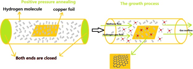
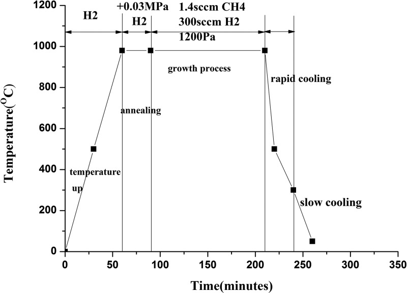
Figure 1 shows schematically the growth processes. A certain amount of H2 was injected into the furnace tube. Then, both ends of the furnace tube were sealed, insuring that no air would leak into the tube. The amount of the injected H2 gas was controlled to provide a positive pressure between 1 and 2 standard atmospheres inside the tube, when the tube temperature reached the annealing temperature (9). After the H2 infection, the substrates were heated up to 980 °C within 60 min (with the heating rate of about 20 °C/min). Then, the copper foil substrate was preannealed at the temperature for about 30 min. Afterward, the H2 gas flow was introduced into the tube with the flow rate of 300 sccm. In addition at the same time, 1.4 sccm CH4 was brought in for the growth of the graphene film. The time for the growth of graphene was about 140 min.
Figure 1.
Flow diagram for the growth of graphene.
When the growth step was over, the heating system and gas source were turned off and the lid of the tubular furnace was opened to cool the tube to room temperature. The size of the prepared graphene film could be adjusted with the size of the oven’s hearth. In addition, the graphene film with an area of 20 × 30 cm was produced in our work.
The wet transfer method26 was used to transfer the prepared graphene films onto SiO2/Si and Quartz glass sheets for measuring the sheet resistance, carrier mobility, and transmittance. The size of the SiO2/Si and quartz glass sheets was 1.5 cm × 1.5 cm, and the transferred graphene films covered the entire substrate surface.
2.3. Fabrication of the Graphene/Si Solar Cells
To demonstrate the quality of the graphene films prepared with our method, the graphene/Si (G/Si) solar cells were fabricated with the prepared monolayer graphene grown on oxygen-free copper foils. The structure of the cell is shown in Figure 2, in which the layers, from the top to bottom, are graphene film, gold/titanium (Au/Ti), alumina (Al2O3), silicon (Si),and aluminum (Al). The cell fabrication process was briefly as follows. A mask plate of 25 mm2 (5 mm × 5 mm) was first put on the middle of the front surface of an n-type doped silicon wafer (⟨100⟩, 0.5 mm, resistivity: 1–10 Ω cm) of a size of 1 cm × 1 cm. Then, the front surface of the wafer was coated with a 100 nm alumina (Al2O3) layer by using a high vacuum multitarget magnetron sputtering coating machine. Subsequently, gold/titanium (Au/Ti) and aluminum (Al) electrodes were evaporated to provide Ohmic contacts on the front and back sides, respectively. Next, the mask plate was removed, leaving a square window, and the produced monolayer graphene film was transferred onto the Si substrate, covering the entire window and tightly contacting with the Si wafer. To demonstrate the uniformity of the prepared graphene films at the same time, six Gr/Si solar cells were fabricated with their graphene layers intercepted from the produced graphene film of large size deposited on the large size copper foil substrate.
Figure 2.
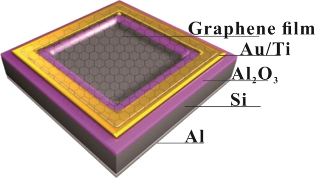
Model of the solar device.
2.4. Characterization
The pretreated foil substrate surface, prepared graphene films, and fabricated Si/graphene solar cells were characterized using appropriate methods as follows. A horizontal high power X-ray powder diffractometer (XRD) (model: TTR-III) was used to analyze the structure of the copper foil surface after negative and positive pressure annealing.
A field-emission scanning electron microscope (model: JEOL JSM-6700F) was used to observe the microstructure of the synthesized graphene.
Raman spectra of the prepared films were measured using HORIBA Jobon Yvon micro-Raman spectrometer (model: LabRAM 800HR). The layer number and large-scale uniformity of graphene samples could be determined by the spectral characteristics.
Visible spectrophotometer (Shanghai Shunyu constant company, Instrument model 723PC) was used to measure the light transmittance of the graphene film transferred from the copper substrate to Quartz glass sheet.
The hall Effect measurement system (ECOPIA Co., Ltd., model: HMS-5000) was used to measure sheet resistance and carrier mobility of the prepared graphene in the van der Pauw configuration with a 0.56 T magnetic field.
Zolix SS150 Solar Simulator is used to test the performance parameters of the solar cells, such as photoelectric conversion efficiency, open circuit voltage, short circuit current, and filling factor.
3. Results and Discussion
We examined systematically the Graphene films deposited on the copper foils annealed under positive pressure. Figure 3a–d shows the SEM images of the graphene films (on the silicon substrates), which were respectively grown on copper foils A–D under the conditions of an optimizing the gas ratio and growth time. The images indicated that thus deposited graphene films covered the entire surface of substrates, and films were continuous and their uniformity was good. In this case, we could prepare graphene films with a monolayer proportion of 95% or more. Figure 3e,f shows partial enlarged views corresponding to images a–d. From the images, we could see that the graphene films have less dark area (dark areas are multilayered) and have almost uniform color. The number of the carbon atom layer of the graphene film was characterized by Raman.
Figure 3.
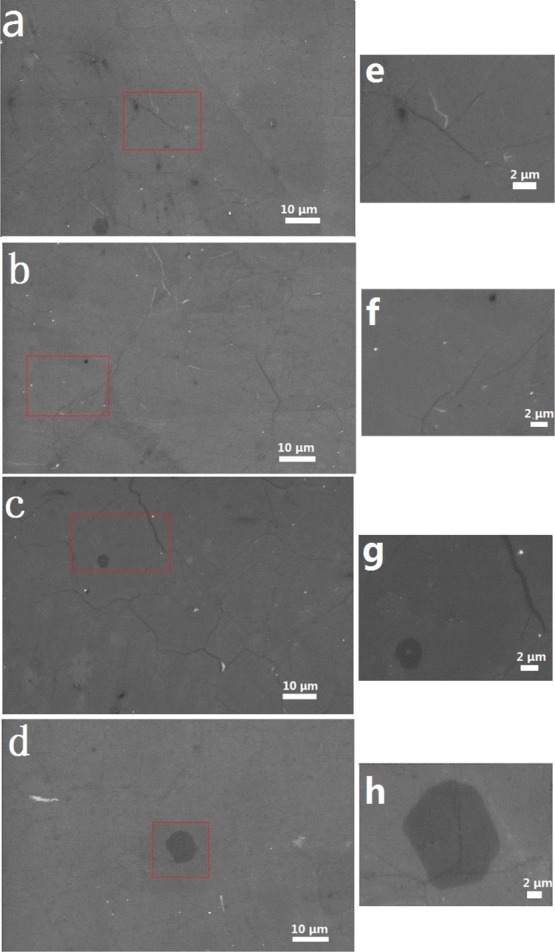
SEM image of monolayer graphene prepared on four copper foils (transferred to Silica wafer). (a) A copper foil, (b) B copper foil, (c) C copper foil, (d) D copper foil; (e–h) Partial enlarged images corresponding to (a–d).
Figure 4a–d displays the Raman spectra of the graphene films grown on the four kinds of copper foils (A–D), each of which contain six spectra corresponding to arbitrarily selected 6 areas of the same graphene film. In each chart, six color curves represent the spectra at six different locations in the graphene. It is known that Raman spectra of graphene materials generally show three major peaks (D peaks: ∼1350 cm–1, G peaks: ∼1580 cm–1, and 2D peaks: ∼2700 cm–1),27 and the D peak was thought to be responsible for the existence of the defects in the sample. Figure 4a–d shows that the spectra nearly has no D peak, which means the prepared graphene film nearly has no defect. The ratio of I2D/IG in the spectra measured on different areas of the sample are nearly the same (Table S1 in the Supporting Information), reflecting that the films are uniform, consisting of monolayer regions.
Figure 4.
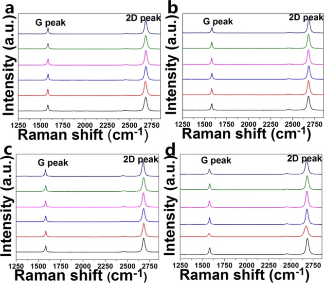
Raman spectra of graphene films grown on (a) “A”, (b) “B”, (c) “C” and (d) “D” copper foils.
Monolayer graphene films grown on the four copper foils (A–D) were transferred to the SiO2/Si substrates to test the sheet resistance and carrier mobility. The statistical histogram of the measured sheet resistances are shown in Figure 5a–d, where the data were recorded from randomly selected 15 test points on each sample. The results show that the sheet resistance are mainly among 500–600 Ω/□. In addition, the Hall measurement showed that the values of the carrier mobility of these samples were 2000–3000 cm2/(V s). The uniformity of sheet resistance and carrier mobility over the whole layer implies higher lattice quality of the prepared graphene films.
Figure 5.
Sheet resistance of the monolayer graphene grown on the four kinds of copper foils: (a) A substrate; (b) B substrate; (c) C substrate; and (d) D substrate.
However, it was found that the growth conditions of graphene for the four kinds of copper foils, preannealed under positive H2 pressure (less than 2 atm), were wider than negative preannealed substrates to produce high-quality graphene films, which would be very conducive to the industrial production. In particular, the suitable annealing time is around 30–120 min, which is as that used for low-pressure annealing. The growth results are not good when the annealing time is too short or too long. This may be explained as follows: the recrystallization of the copper foil has not yet been completed, if the annealing time is too short; to the opposite, if the annealing time is too long, then the evaporation of copper foil will be too serious, leading to production of more defects in copper.
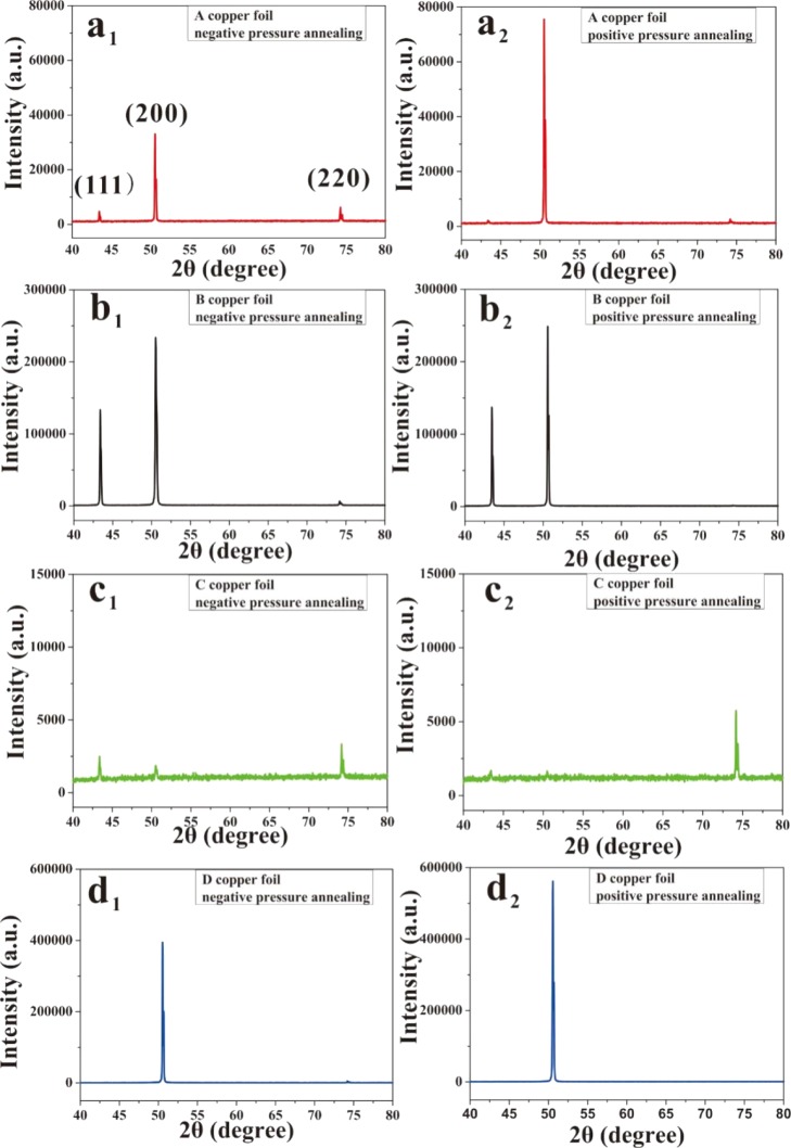
Our results demonstrated that the positive pressure annealing of the cooper substrates is more favorable for graphene deposition. To understand the mechanism, the surface crystalline structures of the four types of cooper substrates annealed under positive and negative H2 pressure were compared. Figure 6 shows the XRD spectra of the four kinds of copper foils, where Figure 6a–d is respectively for foils A–D, and the subscripts 1 and 2 indicate the foils were annealed respectively under the ambient of negative H2 pressure (N-A) and positive H2 pressure (P-A). For all four kinds of foils, the spectra show three peaks (111), (200), and (220), but their intensities differ considerably for foils treated with N-A and P-A. Figure 6a1,a2 shows the recorded XRD spectra of “A” copper foils after N-A and P-A, respectively. It is found that, different from the spectra of the N-A-treated sample, for the sample after P-A treatment, the intensities of (220) and (111) peaks were weakened, whereas the intensity of (200) peak was enhanced considerably. The results for “B” copper foil (Figure 6b1,b2) show that for the XRD spectra (Figure 6b2) of the foil treated through P-A, the intensities of (111) and (200) peaks were enhanced, and the (220) peak disappeared in comparison with that of N-A-treated foil B. The results for the “C” copper foil (Figure 6c1,c2) display that after P-A, the (111) and (200) peaks nearly disappeared, and the (220) peak was enhanced a lot. In addition, the results for “D” copper foil (Figure 6d1,d2) show that after P-A, the (220) peak disappeared, and the (200) peak was enhanced with respect to the N-A-treated foil. The results mentioned above demonstrated that the P-A-treated copper foil, compared with the N-A-treated foil, exhibited better crystallinity and the preferential orientation, which would be more favorable for the growth of graphene (large area and single crystalline).
Figure 6.
XRD spectra of the four kinds of copper foils pretreated with N-A and P-A: (a–d) denote the foil types A–D, respectively, and the subscripts 1 and 2 denote the corresponding foils that underwent negative and positive H2 pressure annealing, respectively.
Figure 7 shows the optical photographs of the graphene-copper foil (copper foil annealed under negative pressure). In Figure 7a–c, the places that are not covered with graphene were oxidized and showed the color of copper oxide. In Figure 7d, the copper foil is α copper foil, which could prepare large area and continuous films under negative pressure and certain parameters as has been reported in many papers. Figure 8 shows the optical photographs of the graphene/copper foil (copper foil annealed under positive pressure). As could be seen from the pictures, graphene grown on four kinds of copper foils have very good continuity, and graphene film completely covered the surface of the copper foil substrate. By comparison, graphene films with better quality could be prepared on copper foil substrates under positive pressure annealing.
Figure 7.
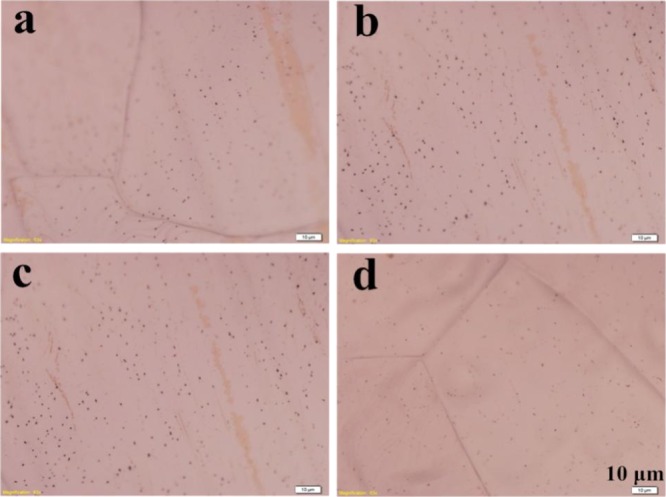
Graphene grown on (a) A copper foil; (b) B copper foil; (c) C copper foil; and (d) D copper foil. (The scale of four pictures is 10 μm).
Figure 8.
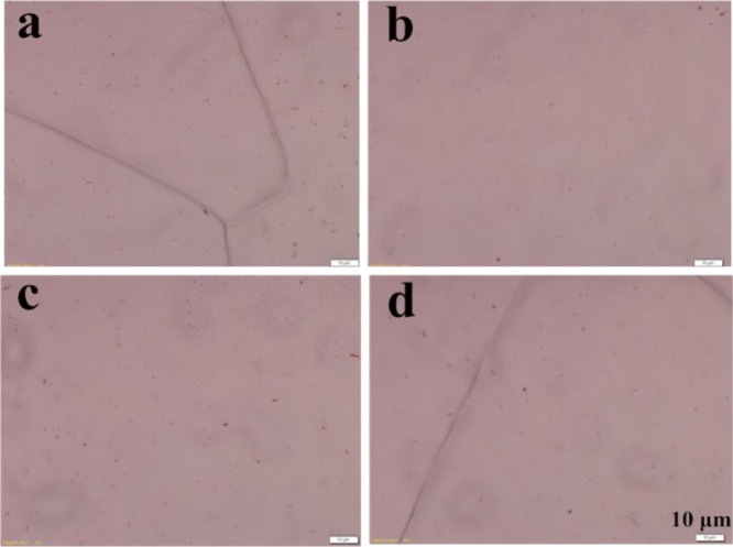
Graphene grown on (a) A copper foil; (b) B copper foil; (c) C copper foil; and (d) D copper foil. (The scale of four pictures is 10 μm).
Figure 9a displays the picture of a 20 cm × 30 cm oxygen-free copper foil (type C) with a graphene layer deposited on its surface. Figure 9b is the optical microscope photograph of the graphene layer (shown in the picture (a)) transferred to a silicon substrate. From the picture, it is seen that the whole grown graphene is continuous and exhibits the same color, implying that almost no multilayer region exists in the grown film. Figure 9c is the Raman spectra recorded from randomly selected 16 sites of the as-grown graphene film on the oxygen-free copper foil. These spectra clearly demonstrate that the grown graphene is basically in monolayer form and the amount of defects is very small. The transmittance of the deposited monolayer graphene film is 97.24% (λ = 550 nm) as shown in Figure 9d. With the method of wet transfer26 and layer superposition, a four layer-superposed graphene film was prepared, of which the sheet resistance was about 80 Ω/sq and the light transmittance was 90.70%. Through the same method, 1–4 layers graphene film were transferred to silicon oxide substrates, as shown in Figure 9e, and the surface resistance was tested. The results are shown in Figure 9f. It could be seen that the surface resistance of 1–4 layers of graphene was reduced from 500 to 80 Ω/sq. These properties of graphene films nearly reached that of the commercialized indium tin oxide (ITO) glasses. The surface resistance of the commercialized ITO glass is in the range of several tens of ohms to several hundred ohms, and the light transmittance is 80% or more. The higher the light transmittance, the larger the sheet resistance is. These results show that the graphene we prepared could be well applied to the transparent conductive electrode.
Figure 9.
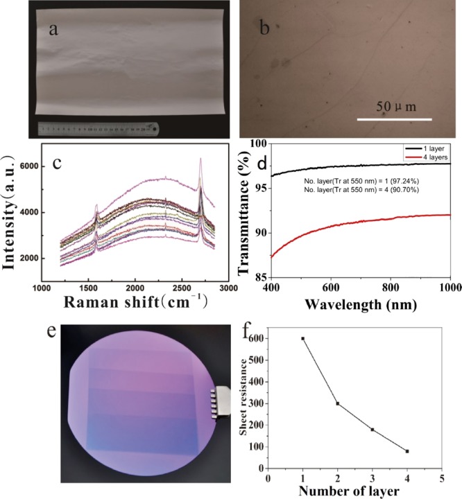
(a) Optical photograph of an as-grown graphene on a oxygen-free copper foil. (b) Microscope photograph of the graphene [the same as in picture (a)] transferred to a silicon substrate. (c) Raman spectra of graphene on a oxygen-free copper foil as shown in figure (a). (d) Transmittance of the monolayer and superposed four layers of graphene film transferred onto the quartz glass sheets. (e) 1–4 layers of graphene film transferred to silicon oxide substrate. (f) Sheet resistance of 1–4 layers graphene film.
It was possible to synthesize single-crystal graphene domains by controlling the growth condition. We prepared single-crystal graphene by adjusting the growth condition parameters. As shown in the Figure S1, the diameter of the prepared single-crystal graphene was about 500 μm.
Figure 10 shows the current density (J)–voltage (V) characteristics of the Gr/Si solar cells. As seen from the figure, the curves for the six solar cells are similar to each other and with only a small dispersion. From the figure, the performances of the cells were derived, and the results are summarized in Table 1. It can be seen that all of the cells have similar performances. These results evidenced qualities of different parts of the graphene film that were nearly the same, which indicated that the graphene film prepared in this work was quite uniform.
Figure 10.
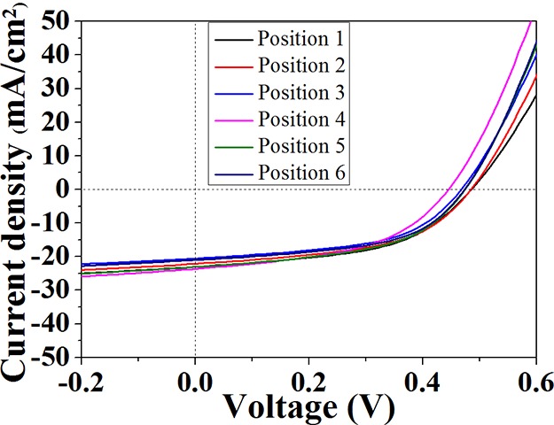
J–V characteristics of as-fabricated G/Si solar cells.
Table 1. Open-Circuit Voltage (Voc), Short-Circuit Current (Jsc), Fill Factor, and Energy Conversion Efficiency (PCE) of the Six Solar Cells Fabricated in the Work.
| Voc (V) | Jsc (mA/cm2) | fill factor (%) | PCE (%) | |
|---|---|---|---|---|
| position 1 | 0.48 | 22.91 | 51.08 | 5.62 |
| position 2 | 0.48 | 21.96 | 51.57 | 5.43 |
| position 3 | 0.46 | 20.44 | 53.07 | 4.99 |
| position 4 | 0.44 | 23.47 | 48.63 | 5.02 |
| position 5 | 0.47 | 22.94 | 51.13 | 5.51 |
| position 6 | 0.47 | 20.93 | 53.07 | 5.22 |
4. Conclusions
The positive pressure H2 ambience annealing method was proposed and used to pretreat the cooper foil substrates for graphene deposition. The results demonstrated that high-quality, large-area graphene films could be deposited on different types of cooper foil substrates by using the proposed substrate preannealing method. The sheet resistances of the obtained graphene films are all about 500 Ω/□. In addition, the coverage of the monolayer graphene film on the substrates could be more than 95.00%. The transmittance of the produced monolayer graphene film is as high as 97.24%. The electron mobility of the graphene films grown on the four types of copper foils was in the range of 2000–3000 cm2/(V s). The prepared graphene films were used to fabricate graphene/silicon solar cells. The energy conversion efficiencies of all of the fabricated cells were between 4.99 and 5.62%, which also illustrated the continuity and uniformity of the prepared graphene films. The advantage of the proposed method was preliminarily analyzed, which could be attributed to the better crystallization orientation of the copper foils under positive pressure H2 ambience annealing.
Acknowledgments
We thank Professor Li-Ren Lou for his help in the preparation of this paper. This work was supported by the National Natural Science Foundation of China (grant nos. 11374280, 50772110).
Supporting Information Available
The Supporting Information is available free of charge on the ACS Publications website at DOI: 10.1021/acsomega.8b02538.
Ratio of I2D/IG for each Raman spectrum and single-crystal graphene domain image (PDF)
Author Contributions
† Q.Y. and Z.Z. are the co-authors of this manuscript.
The authors declare no competing financial interest.
Supplementary Material
References
- Morozov S. V.; Novoselov K. S.; Katsnelson M. I.; Schedin F.; Elias D. C.; Jaszczak J. A.; Geim A. K. Giant intrinsic carrier mobilities in graphene and its bilayer. Phys. Rev. Lett. 2008, 100, 016602. 10.1103/physrevlett.100.016602. [DOI] [PubMed] [Google Scholar]
- Balandin A. A.; Ghosh S.; Bao W.; Calizo I.; Teweldebrhan D.; Miao F.; Lau C. N. Superior thermal conductivity of single-layer graphene. Nano Lett. 2008, 8, 902–907. 10.1021/nl0731872. [DOI] [PubMed] [Google Scholar]
- Lee J.-U.; Yoon D.; Cheong H. Estimation of Young’s Modulus of Graphene by Raman Spectroscopy. Nano Lett. 2012, 12, 4444–4448. 10.1021/nl301073q. [DOI] [PubMed] [Google Scholar]
- Nair R. R.; Blake P.; Grigorenko A. N.; Novoselov K. S.; Booth T. J.; Stauber T.; Peres N. M. R.; Geim A. K. Fine structure constant defines visual transparency of graphene. Science 2008, 320, 1308. 10.1126/science.1156965. [DOI] [PubMed] [Google Scholar]
- Novoselov K. S.; Geim A. K.; Morozov S. V.; Jiang D. A.; Zhang Y.; Dubonos S. V.; Grigorieva I. V.; Firsov A. A. Electric field effect in atomically thin carbon films. Science 2004, 306, 666–669. 10.1126/science.1102896. [DOI] [PubMed] [Google Scholar]
- Yu Q.; Lian J.; Siriponglert S.; Li H.; Chen Y. P.; Pei S.-S.; Siriponglert S. Graphene segregated on Ni surfaces and transferred to insulators. Appl. Phys. Lett. 2008, 93, 113103. 10.1063/1.2982585. [DOI] [Google Scholar]
- Reina A.; Jia X.; Ho J.; Nezich D.; Son H.; Bulovic V.; Dresselhaus M. S.; Kong J. Large Area, Few-Layer Graphene Films on Arbitrary Substrates by Chemical Vapor Deposition. Nano Lett. 2009, 9, 3087. 10.1021/nl901829a. [DOI] [PubMed] [Google Scholar]
- Kim K. S.; Zhao Y.; Jang H.; Lee S. Y.; Kim J. M.; Kim K. S.; Ahn J.-H.; Kim P.; Choi J.-Y.; Hong B. H. Large-scale pattern growth of graphene films for stretchable transparent electrodes. Nature 2009, 457, 706–710. 10.1038/nature07719. [DOI] [PubMed] [Google Scholar]
- Li X.; Cai W.; An J.; Kim S.; Nah J.; Yang D.; Piner R.; Velamakanni A.; Jung I.; Tutuc E.; et al. Large-Area Synthesis of High-Quality and Uniform Graphene Films on Copper Foils. Science 2009, 324, 1312–1314. 10.1126/science.1171245. [DOI] [PubMed] [Google Scholar]
- Hummers W. S.; Offeman R. E. Preparation of Graphitic Oxide. J. Am. Chem. Soc. 1958, 80, 1339. 10.1021/ja01539a017. [DOI] [Google Scholar]
- Qian W.; Hao R.; Hou Y.; Tian Y.; Shen C.; Gao H.; Liang X. Solvothermal-Assisted Exfoliation Process to Produce Graphene with High Yield and High Quality. Nano Res. 2009, 2, 706–712. 10.1007/s12274-009-9074-z. [DOI] [Google Scholar]
- Wofford J. M.; Nie S.; McCarty K. F.; Bartelt N. C.; Dubon O. D. Graphene Islands on Cu Foils: The Interplay between Shape, Orientation, and Defects. Nano Lett. 2010, 10, 4890–4896. 10.1021/nl102788f. [DOI] [PubMed] [Google Scholar]
- Li X.; Magnuson C. W.; Venugopal A.; An J.; Suk J. W.; Han B.; Borysiak M.; Cai W.; Velamakanni A.; Zhu Y.; Fu L.; et al. Graphene Films with Large Domain Size by a Two-Step Chemical Vapor Deposition Process. Nano Lett. 2010, 10, 4328–4334. 10.1021/nl101629g. [DOI] [PubMed] [Google Scholar]
- Liu N.; Fu L.; Dai B.; Yan K.; Liu X.; Zhao R.; Zhang Y.; Liu Z. Universal Segregation Growth Approach to Wafer-Size Graphene from Non-Noble Metals. Nano Lett. 2011, 11, 297–303. 10.1021/nl103962a. [DOI] [PubMed] [Google Scholar]
- Yao Y.; Li Z.; Lin Z.; Moon K.-S.; Agar J.; Wong C. Controlled Growth of Multilayer, Few-Layer, and Single-Layer Graphene on Metal Substrates. J. Phys. Chem. C 2011, 115, 5232–5238. 10.1021/jp109002p. [DOI] [Google Scholar]
- Robertson A. W.; Warner J. H. Hexagonal Single Crystal Domains of Few-Layer Graphene on Copper Foils. Nano Lett. 2011, 11, 1182–1189. 10.1021/nl104142k. [DOI] [PubMed] [Google Scholar]
- Sutter P. W.; Flege J.-I.; Sutter E. A. Epitaxial graphene on ruthenium. Nat. Mater. 2008, 7, 406–411. 10.1038/nmat2166. [DOI] [PubMed] [Google Scholar]
- Yan Z.; Lin J.; Peng Z.; Sun Z.; Zhu Y.; Li L.; Xiang C.; Samuel E. L.; Kittrell C.; Tour J. M. Toward the synthesis of wafer-scale single-crystal graphene on copper foils. ACS Nano 2012, 6, 9110–9117. 10.1021/nn303352k. [DOI] [PubMed] [Google Scholar]
- Hao Y.; Bharathi M. S.; Wang L.; Liu Y.; Chen H.; Nie S.; Wang X.; Chou H.; Tan C.; Fallahazad B.; et al. The role of surface oxygen in the growth of large single-crystal graphene on copper. Science 2013, 342, 720–723. 10.1126/science.1243879. [DOI] [PubMed] [Google Scholar]
- Zhou H.; Yu W. J.; Liu L.; Cheng R.; Chen Y.; Huang X. Q.; Liu Y.; Wang Y.; Huang Y.; Duan X. F. Chemical vapour deposition growth of large single crystals of monolayer and bilayer graphene. Nat. Commun. 2013, 4, 2096. 10.1038/ncomms3096. [DOI] [PubMed] [Google Scholar]
- Mohsin A.; Liu L.; Liu P.; Deng W.; Ivanov I. N.; Li G.; Dyck O. E.; Duscher G.; Dunlap J. R.; Xiao K.; Gu G. Synthesis of millimeter-size hexagon-shaped graphene single crystals on resolidified copper. ACS Nano 2013, 7, 8924–8931. 10.1021/nn4034019. [DOI] [PubMed] [Google Scholar]
- Chen S.; Ji H.; Chou H.; Li Q.; Li H.; Suk J. W.; Piner R.; Liao L.; Cai W.; Ruoff R. S. Millimeter size single crystal graphene by suppressing evaporative loss of Cu during low pressure chemical vapor deposition. Adv. Mater. 2013, 25, 2062–2065. 10.1002/adma.201204000. [DOI] [PubMed] [Google Scholar]
- Wang H.; Xu X.; Li J.; Lin L.; Sun L.; Sun X.; Zhao S.; Tan C.; Chen C.; Dang W.; et al. Surface Monocrystallization of Copper Foil for Fast Growth of Large Single-Crystal Graphene under Free Molecular Flow. Adv. Mater. 2016, 28, 8968–8974. 10.1002/adma.201603579. [DOI] [PubMed] [Google Scholar]
- Xu X.; Zhang Z.; Dong J.; Yi D.; Niu J.; Wu M.; Lin L.; Yin R.; Li M.; Zhou J.; et al. Ultrafast epitaxial growth of metre-sized single-crystal graphene on industrial Cu foil. Sci. Bull. 2017, 62, 1074–1080. 10.1016/j.scib.2017.07.005. [DOI] [PubMed] [Google Scholar]
- Liu L.; Zhou H.; Cheng R.; Yu W. J.; Liu Y.; Chen Y.; Shaw J.; Zhong X.; Huang Y.; Duan X. High-yield chemical vapor deposition growth of high-quality large-area AB-stacked bilayer graphene. Acs Nano 2012, 6, 8241–8249. 10.1021/nn302918x. [DOI] [PMC free article] [PubMed] [Google Scholar]
- Li X.; Zhu Y.; Cai W.; Borysiak M.; Han B.; Chen D.; Piner R. D.; Colombo L.; Ruoff R. S. Transfer of Large-Area Graphene Films for High-Performance Transparent Conductive Electrodes. Nano Lett. 2009, 9, 4359–4363. 10.1021/nl902623y. [DOI] [PubMed] [Google Scholar]
- Malard L. M.; Pimenta M. A.; Dresselhaus G.; Dresselhaus M. S. Raman spectroscopy in graphene. Phys. Rep. 2009, 473, 51–87. 10.1016/j.physrep.2009.02.003. [DOI] [Google Scholar]
Associated Data
This section collects any data citations, data availability statements, or supplementary materials included in this article.


