Abstract
Since the recent experimental discovery of the CrI3 and CrGeTe3 monolayers, van der Waals (vdW) layered transition metal compounds have been recognized as promising candidates to realize 2D ferromagnetic (FM) semiconductors. However, until now, only limited compounds have been proposed to be ferromagnetic semiconductors. Here, on the basis of first-principles calculations, we report that the monolayer, Janus monolayer, and bilayer of NiX2 (X = Cl, Br, I) are intrinsic 2D FM semiconductors. Our results show that exfoliation energy of the NiX2 monolayer is smaller than that of graphene, and all studied NiX2 layers show semiconducting band gaps. The predicted Curie temperature values for NiX2 (X = Cl, Br, I) monolayers ranged from 120 to 170 K with Monte Carlo simulations. For the Janus monolayer, we found that the spin interaction shows a very strong magnetoelectric coupling under an external electric field. Furthermore, for the bilayer of NiX2, our results show that the interlayer coupling is quite weak, indicating the possibility of tuning the magnetic coupling through external manipulations.
Introduction
During the past decade, two-dimensional (2D) materials, such as graphene,1 h-BN,2 MoS2,3 and black phosphorus,4 have received much attention because of their unique properties and potential applications in future nanodevices.5 Magnetism, especially in 2D systems, is one of the most fascinating properties of materials, not only because of the complex magnetic behavior itself but also due to its interplay with the other important properties of materials such as superconductivity, ferroelectricity, and quantum Hall effects. However, in early studies, long-range magnetic order is predicted to be prohibited in a 2D system according to the Mermin–Wagner theorem.6 Recently, Gong et al.7and Huang et al.8 reported their discovery of long-range ferromagnetic (FM) order in 2D intrinsic semiconductors, Cr2Ge2Te6 and CrI3, which are exfoliated down to atomically thin layers from their van der Waals (vdW) layered bulk materials. These exciting findings promote the studies of 2D magnetic semiconductors to a new stage. But the measured Curie temperature (TC) values of these materials are very low (<45 K), which badly hinders their practical applications in spintronic devices.
Tremendous efforts have been devoted to realize ferromagnetic order in 2D semiconductors with higher Curie temperature. For example, embedding transition metal atoms and applying strain, defects, or boundaries9−13 have been adopted as a strategy to induce magnetism in a nonmagnetic system. But these methods are usually difficult to control in an experiment, and the induced ferromagnetism is very weak. Recently, the vdW layered transition metal compounds have been recognized as promising candidates to realize 2D FM semiconductors because these materials usually possess intrinsic magnetism and can be easily exfoliated down to monolayers. Several 2D systems have been confirmed to be intrinsic FM materials such as VSe2,14 MnSe2,15 FePS3,16 and MnO2,17 but all these materials are metallic. 2D FM semiconductors are still very rare, and their TC values are much below room temperature because the virtual exchange interactions in a semiconductor are usually much weaker than the carrier-driven exchange interactions in a metallic system. Thus, to better understand the intrinsic mechanism of ferromagnetic semiconductors, it becomes more and more important to explore new families of semiconducting monolayers with ferromagnetism.
Here, on the basis of first-principles calculations, we predict that the family of NiX2 (X = Cl, Br, I) layers can be promising 2D intrinsic FM semiconductors. Our results show that exfoliation energy of the NiX2 monolayer is smaller than that of graphene, and all the NiX2 monolayers show semiconducting band gaps, which vary from 1.24 to 2.60 eV. Their Curie temperature (TC) values were predicted from 120 to 170 K with Monte Carlo simulations. For the Janus monolayer, we found that the spin interaction shows a very strong magnetoelectric coupling. Furthermore, for the bilayer of NiX2, our results show that the interlayer coupling is quite weak, indicating the possibility of tuning the magnetic coupling through external manipulations.
Results and Discussion
The large interlayer distance between vdW layers (3.08, 3.28, and 3.35 Å for NiCl2, NiBr2, and NiI2, respectively) of NiX2 bulks implies a weak interlayer interaction between layers and the possibility to obtain 2D monolayers with a suitable exfoliation method. To demonstrate this, two fundamental questions should be taken into account. One is the cleavage energy, which gives a quantitative description of the strength of interlayer binding, and the other one is the in-plane stiffness of the corresponding 2D monolayer, which determines whether the exfoliated monolayer can have a large area and be free-standing. Generally, a small cleavage energy and strong in-plane stiffness are what we need.
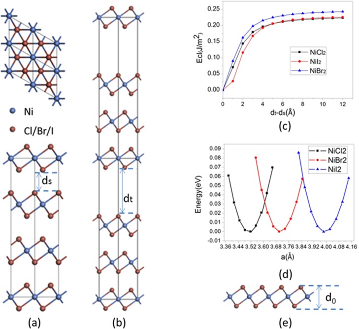
To achieve the 2D monolayer from the vdW bulk crystals, the most commonly used approaches are mechanical cleavage and liquid exfoliation.1,18,19 To confirm that it is possible to exfoliate NiX2 monolayers from their bulk phases in the experiment, we first calculated the cleavage energy. A gradually expanded fracture is introduced in the bulk to simulate the exfoliation procedure (Figure 1a,b).20 As expected, the total energy increases as the separation between two fractured parts increases (Figure 1c). It can be found that the total energy increases rapidly when the separation is less than 3.0 Å. As the separation becomes larger, the total energy barely changes. Then, we find that the cleavage energies for NiCl2, NiBr2, and NiI2 are 0.223, 0.242, and 0.26 J/m2, which are smaller than that for graphite (∼0.36 J/m2),21,22 implying that NiX2 can be easily exfoliated down to the monolayer in the experiment. We also calculate the cleavage energy of bilayer nanosheets and obtain very similar values, which are 0.224, 0.243, and 0.26 J/m2.
Figure 1.
(a) Top (upper panel) and side (bottom panel) views of crystal structure of bulk NiX2 (X = Cl, Br, I). (b) Super cell model with introduced fracture used to simulate the exfoliation procedure. (c) Cleavage energy Ecl as a function of the separation between two fractured parts. (d) Variation of relative energy with the 2D lattice constant for the monolayer of NiX2. The energy of equilibrium state is set to 0. (e) NiX2 monolayer. d0 is the vertical distance between two halide atomic planes.
To obtain a free-standing membrane during the exfoliation process in the experiment, it is important to avoid curling or buckling. To investigate the in-plane stiffness of NiX2 monolayers, the 2D Young’s modulus is evaluated according to the following equation
where E is the total energy per unit cell, a0 is the 2D lattice constant, and A is the corresponding surface area. Figure 1d shows the profile of total energy versus lattice constant a0 for NiX2 monolayers. The 2D Young’s moduli for NiCl2, NiBr2, and NiI2 are calculated to be 54, 50, and 45 N m–1, respectively, which are close to that of the MnPSe323 monolayer and comparable to that of the ultrastrong material graphene (∼340 N m–1).24,25 Further, according to the elastic theory, the typical out-of-plane deformation h induced by gravity can be estimated by the formula25
where p = 2.00 × 10⁻⁶, 3.06 × 10⁻⁶, and 3.78 × 10⁻⁶ kg/m2 are the densities of 2D NiCl2, NiBr2, and NiI2, respectively, and L is the edge length. Assuming that L ≈ 100 μm, we obtain h/L values of 3.31 × 10⁻⁴, 3.91 × 10⁻⁴, and 4.35 × 10⁻⁴ for 2D NiCl2, NiBr2, and NiI2, respectively. These values are of the same order of magnitude as that of graphene.25 These suggest that the NiX2 monolayers are stiff enough to withstand its own weight and keep a free-standing planar structure during exfoliation.
The NiX2 monolayers possess a structure similar to that of the T-MoS2 monolayer, which belong to the P-3m1 layer group. No Jahn–Teller distortion is observed, and each Ni atom is coordinated to six ligands. The structural parameters are listed in Table 1. As the atomic radius increases from NiCl2 to NiI2, the lattice constant a0, bond length of Ni–X atom marked as dNi–X, and vertical distance between two halide planes d0 also increase. The calculated lattice constants a0 of the monolayers are very close to those of their bulks (3.483, 3.699, and 3.983 Å for NiCl2, NiBr2, and NiI2, respectively), suggesting very weak interlayer interactions between vdW layers.
Table 1. Geometrical Parameters of Optimized Monolayers NiX2 (X = Cl, Br, I), Lattice Constant (a0), Bond Length between Atoms Ni and X (dNi–X), and Interlayer Distance between Two Halide Planes (d0).
| compound | a0 (Å) | dNi–X (Å) | d0 (Å) |
|---|---|---|---|
| NiCl2 | 3.518 | 2.424 | 2.648 |
| NiBr2 | 3.700 | 2.573 | 2.868 |
| NiI2 | 3.983 | 2.775 | 3.107 |
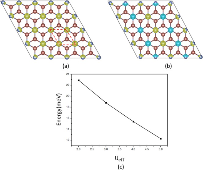
In NiX2 monolayers, because of the octahedral crystal field caused by the ligands, the Ni d orbitals split into two parts, namely, the lower t2g and the higher eg manifolds. Each Ni gives two electrons to form ionic bonding with the ligands and leaves eight electrons, which fully occupy the t2g orbitals and the spin-up eg orbitals, and the spin-down eg orbitals are empty. Thus, the Ni2+ ion shows an occupation state of d8 with a magnetic moment of ∼2 μB. A sizable electronic band gap is expected to be opened by the crystal field. To determine the magnetic ground state of monolayer NiX2, we carry out spin-polarized calculations. Two different magnetic configurations are considered in a 2 × 1 super cell, that is, the FM state and antiferromagnetic (AFM) state. The spin densities for these two states are shown in Figure 2a,b. The spin polarizations are mainly contributed by Ni ions, while the ligands are slightly spin-polarized. The projected magnetic moment on each Ni ion is nearly the same for FM and AFM states. The numerical results are listed in Table 2. It is found that the FM states for NiCl2, NiBr2, and NiI2 monolayers are lower in energy than the corresponding AFM states by 11.2, 12.6, and 15.4 meV per unit cell, respectively, suggesting that the ground states are FM; this is consistent with recent studies reported by Mounet et al.26
Figure 2.
Spin density (isovalue of 0.025 e/Å3) of (a) the FM state and (b) AFM state. Yellow and blue isosurfaces represent net spin-up and spin-down charge densities, respectively. The rhombic primitive cell is marked by a red dotted line. (c) Change of exchange energy of monolayer NiI2 with respect to different values of Ueff.
Table 2. Projected Magnetic Moment on Each Ni Site (Mu), Exchange Energy (Eex), Electronic Band Gap (Eg), Nearest-Neighboring Exchange Parameter (J), and Curie Temperature (TC).
| compound | Mu (μB) | Eex (eV) | Eg (eV) | J (meV) | TC (K) |
|---|---|---|---|---|---|
| NiCl2 | 1.63 | 11.2 | 2.60 | 2.8 | ∼120 |
| NiBr2 | 1.57 | 12.6 | 1.97 | 3.2 | ∼140 |
| NiI2 | 1.46 | 15.4 | 1.24 | 3.9 | ∼170 |
It is known that the results from GGA + U calculations for a magnetic system sometimes may depend on the adopted value of effective Hubbard U (Ueff). Thus, to verify our result, we repeat the GGA + U calculations with Ueff = 2–5 eV for Ni d orbitals for the NiI2 monolayer. The ground state remains FM with exchange energy ranging from 12 to 23 meV. Thus, the predicted ferromagnetism in NiI2 is robust against the value of Hubbard U.
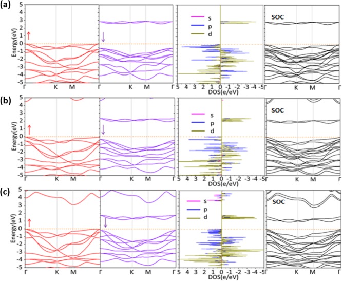
Figure 3 shows the electronic structures of FM ground states for NiX2 monolayers. Here, we focus on the results calculated by the PBE + U method. The effect of spin-orbit coupling (SOC) can be further elucidated by comparing the electronic band structure, as shown in Figure 3. It is found that all the three systems are semiconductors with indirect band gaps of 2.60, 1.97, and 1.24 eV for NiCl2, NiBr2, and NiI2, respectively, consistent with our above analysis. The decrease in band gap from NiCl2 to NiI2 is due to the decrease in strength of the crystal field, which is inversely proportional to the Ni–X bond length. Interestingly, the value of exchange energy increases from NiCl2 to NiI2. This may be caused by two factors: (i) The reduction of energy gap between t2g and eg orbitals will strengthen the t2g–eg virtual exchange interaction, benefiting the FM coupling, which has been carefully discussed in our previous work.27 (ii) I has a smaller electronegativity than Cl, namely, the on-site energy of I p orbitals is closer to that of Ni d orbitals than the Cl p orbitals do. Thus, the d–p–d superexchange in NiI2 is stronger than that in NiCl2, which can be confirmed by comparing the PDOS between NiI2 and NiCl2, where the broadening of Ni d orbitals in energy for NiI2 is larger than that for NiCl2. Similar phenomena are also found in previous studies on transition metal halides monolayers such as CrX328 and VX3.29 After considering SOC, there is no noticeable change in the electronic band structure, as shown in Figure 3, with the indirect band gaps of 2.57, 1.82, and 1.03 eV for NiCl2, NiBr2, and NiI2, respectively.
Figure 3.
Band structure and corresponding density of states of (a) NiCl2, (b) NiBr2, and (c) NiI2 monolayers.
For practical spintronic applications of 2D FM semiconductors, it is necessary to investigate the magnetic behavior under finite temperature. The Ising model has been widely used to describe the magnetic coupling in 2D magnetic systems.17,30−32 Here, we also use the Ising model including nearest-neighboring exchange interactions to study the magnetic behavior of NiX2 (X = Cl, Br, I) monolayers. The spin Hamiltonian
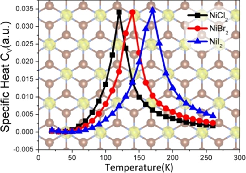
where the summation i runs over all Ni sites, j runs over the six nearest neighbors of site i. Jij is the nearest-neighboring exchange parameter. Then, we performed Metropolis Monte Carlo simulations33,34 to estimate the TC. A 30 × 30 hexagonal superlattice containing 900 magnetic sites and the periodic boundary condition is used. The average magnetization per formula unit and the specific heat [Cv = (⟨E2⟩ – ⟨E⟩2)/kBT2] are taken after the system reaches the equilibrium state at a given temperature (Figure 4). The TC can also be extracted from the peak of the specific heat profile.35 The estimated TC values for NiX2 (X = Cl, Br, I) monolayers are 120, 140, and 170 K, respectively, which are much larger than the reported values for 2D CrI3 (∼45 K)8 and Cr2Ge2Te6 (∼30 K)7 and are higher than the liquid nitrogen temperature (77 K).
Figure 4.
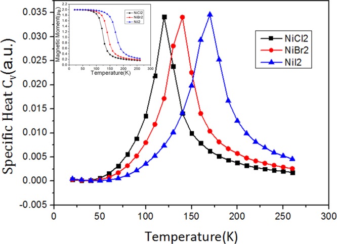
Specific heat Cv with respect to temperature for the NiCl2, NiBr2, and NiI2 monolayers; the inset shows the corresponding magnetization.
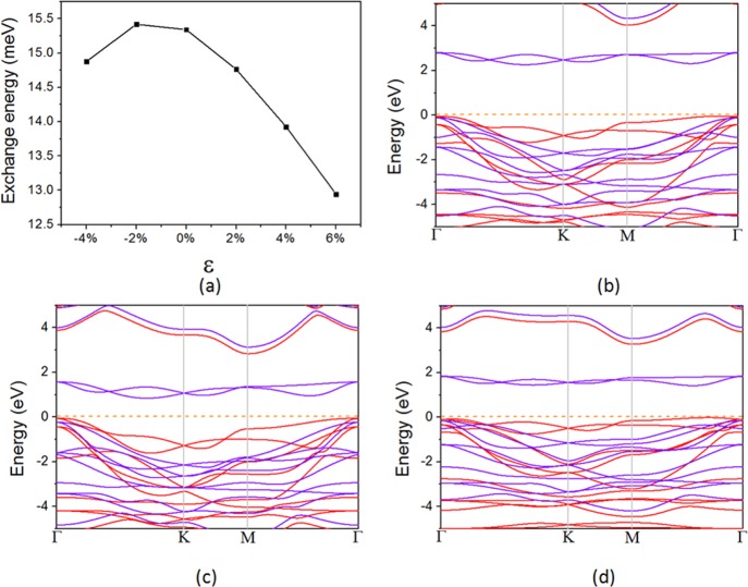
For practical uses, a 2D material usually needs to be supported by a suitable substrate, which may apply an in-plane strain and affect the performance of the pristine material. Thus, it is necessary to investigate the magnetic and electronic properties of NiX2 monolayers under a proper in-plane strain. Here, we focus on NiI2 because it has the highest TC among the three systems. The applied biaxial in-plane strain is defined as ε = (a – a0)/a0 × 100%, where a0 and a are the lattice constants of 2D NiI2 in its equilibrium and strained states, respectively. Positive and negative values of ε represent tensile and compressive strain, respectively. As shown in Figure 5a, a tensile strain will reduce the exchange energy. This is opposite to previous studies on CrI328 and CrGeTe350 where the exchange energy is increased by a tensile strain. It can be understood that the Cr3+ ion in CrI3 and CrGeTe3 has a d3 occupation state, which is less than half-filled. In this case, the AFM direct exchange mainly contributed by the t2g–t2g hybridizations, which can be fairly reduced by a tensile in-plane strain that increases the distance between neighboring Cr3+ ions. Thus, a proper tensile in-plane strain can enhance the FM couplings in CrI3 and CrGeTe3. But in NiI2, the occupation state of Ni2+ (d8) is more than half-filled. In this case, the AFM direct exchange originates from eg–eg hybridizations, which is usually much weaker than the t2g–t2g hybridizations and is not sensitive to a tensile strain, while the tensile strain reduces the d–p exchange interactions, weakening the FM couplings between adjacent Ni2+ ions. When applying a compressive strain, the exchange energy decreases. This is mainly because a compressive strain will strengthen the crystal field, increasing the energy gap between t2g and eg orbitals (Figure 5c) and weakening the FM t2g–eg virtual exchange interactions. The indirect band gaps of NiI2 under −4 and 4% strain are 0.90 and 1.43 eV, respectively. Overall, the electronic and magnetic properties of NiI2 only slightly change under a moderate in-plane strain, which makes it a robust 2D FM semiconductor. PBE functional is known to usually underestimate the band gap; thus, we also repeat our calculation using HSE06 hybrid functional for NiI2 monolayer. The band structure of NiI2 calculated by HSE06 functional is also shown in Figure 5b, with an indirect band gap of 2.31 eV nearly twice as large as the one (1.24 eV) calculated by the PBE + U method. Also, the ground state is also FM with an exchange energy of 19.5 meV, which is a bit larger than the PBE + U result (15.4 meV).
Figure 5.
(a) Change of exchange energy with respect to the in-plane biaxial strain. (b) Band structure of NiI2 calculated by HSE06 hybrid functional. (c) Band structure of NiI2 under −4% strain. (d) Band structure of NiI2 under 4% strain. The red and purple lines represent the spin-up and spin-down bands, respectively.
Janus 2D materials with breaking mirror or inversion symmetry along out-of-plane orientations provide abundant new properties such as electric polarization and Rashba effect, which expands the promising applications of 2D materials.36−38 Thus, it will be interesting to explore the properties of the Janus NiXY monolayer. Here, we calculated the NiICl monolayer. The calculated lattice constant is 3.74 Å, which is between those of NiI2 and NiCl2. The breaking of inversion symmetry can be seen from the optimized structure (Figure 6a). This induces a vertical electric polarization of 0.19 C/m2, making NiICl a 2D multiferroic material. The magnetic ground state is also FM for NiICl, with an exchange energy of 9.3 meV. Interestingly, because of out-of-plane electric polarization, the response of magnetic coupling to a vertical external electric field also exhibits a “polar” behavior; that is, an electric field along the +z direction will enhance the FM coupling, while an electric field along the −z direction will weaken it (Figure 6b). On the other hand, the electronic structure of NiICl does not change much compared to that of the NiI2 monolayer (Figure 6c).
Figure 6.
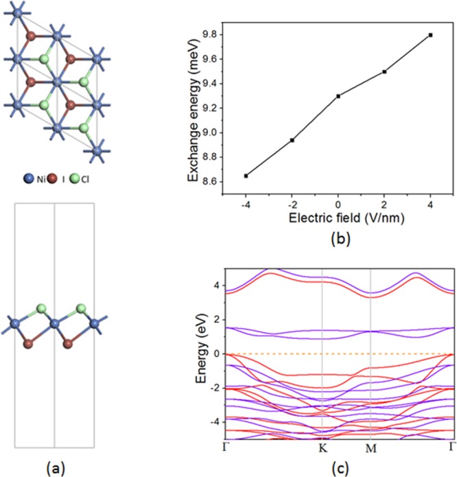
(a) Top (upper panel) and side (bottom panel) views of crystal structure of NiICl. (b) Change of exchange energy with respect to electric field. (c) Band structure of NiICl. The red and purple lines represent the spin-up and spin-down bands, respectively.
On the other hand, 2D magnetic materials are usually used as a building block of vdW heterostructures and junctions to realize a highly functional nanodevice. For instance, the recently discovered 2D FM semiconductor CrI3 shows AFM interlayer magnetic couplings in bilayer CrI3. This unusual property has attracted much attention. Thus, it is also important to explore the interlayer interactions between NiX2 layers. Here, AA- and AB-stacked bilayers of NiCl2, NiBr2, and NiI2 are considered in our calculations. The AB-stacked bilayers are more favored than the AA-stacked ones with total energy values lower by 0.001, 0.001, and 0.002 eV for NiCl2, NiBr2, and NiI2, respectively. The lattice constants a0 of AB-stacked bilayers NiCl2, NiBr2, and NiI2 are 3.49, 3.70, and 4.01 Å, which are very close to their bulks, suggesting weak vdW interlayer interactions between layers.
For the magnetic coupling in such bilayer systems, two different magnetic configurations are considered, that is, the FM state and the interlayer-antiferromagnetic (I-AFM, where Ni ions in one layer possess spin-up magnetic moment and, in the other layer, possess spin-down magnetic moment) state. We find that the FM states are lower in energy than the I-AFM states. But the energy differences between FM and I-AFM states are very small, which are 0.27, 0.65, and 2.20 meV for AB stacking (0.17, 0.47, and 1.42 meV for AA stacking), suggesting that the magnetic coupling between NiX2 layers can be easily tuned by external perturbations.
Conclusions
In summary, on the basis of first-principles calculations, we propose a class of 2D FM semiconductors, the NiX2 (X = Cl, Br, I) monolayers by exfoliation from corresponding vdW bulk materials. The calculated cleavage energy of bulk NiX2 (X = Cl, Br, I) is slightly smaller than that of graphite, indicating that exfoliation is possible in the experiment by mechanical cleavage or liquid exfoliation. Meanwhile, the calculated in-plane stiffness implies that the 2D NiX2 (X = Cl, Br, I) monolayers can keep their free-standing structures without curling or buckling. All three monolayers are semiconducting with band gaps of 2.60, 1.97, and 1.24 eV for NiCl2, NiBr2, and NiI2, respectively. The ground states of the monolayers are FM with TC values ranging from 120 to 170 K. The TC increases from NiCl2 to NiBr2 and NiI2 due to enhanced p–d exchange interactions and t2g–eg virtual exchange interactions. Different from the usual case of tensile strain-induced enhancement of ferromagnetism in systems such as CrI3 and CrGeTe3, FM couplings in NiI2 are slightly decreased by both tensile and compressive strain due to its more than half-filled occupation state. Besides, for the Janus monolayer, we found that the spin interaction shows a very strong magnetoelectric coupling. Furthermore, for the bilayer of NiX2, our results show that the interlayer coupling is quite weak, indicating the possibility of tuning the magnetic coupling through external manipulations. Our findings suggest that NiX2 (X = Cl, Br, I) layers can have promising applications in spintronic devices such as spin valves, information transport, and storage between electric signals and spin signals. We hope that the present study will stimulate further experimental effort on this subject.
Computational Methods
The first-principles calculations based on spin-polarized density functional theory (DFT) are performed using the projected augmented plane-wave (PAW)39 method as implemented in the Vienna ab initio simulation package (VASP).40 Generalized gradient approximation (GGA) given by Perdew–Burke–Ernzerhof (PBE) was adopted for exchange–correlation functionals.41 Considering the strongly correlated electrons in the partially filled d subshells, we use the GGA + U method introduced by Dudarev et al.42 with Ueff = 4 eV for Ni d orbitals. The electronic wave functions are expanded using a plane-wave basis set with a cutoff energy of 500 eV. For 2D monolayer system, a vacuum space of 20 Å along the z direction is adopted to avoid interactions between two neighboring images. The Γ-centered Monkhorst–Pack43−45 point scheme with 8 × 8 × 1 and 4 × 8 × 1 grid meshes is used to sample the reciprocal space of the primitive cell and the 2 × 1 super cell, respectively. For the bulk crystals, the DFT-D3 method by Grimme46 is used to account for the weak vdW interactions between different layers. During the optimization, both the lattice constants and positions of all atoms are relaxed without any symmetry restriction until the Hellmann–Feynman force on each atom is less than 0.01 eV Å–1. The convergent criterion for the total energy is set as 1 × 10⁻⁵ eV.
Acknowledgments
The work is supported by the NSFC (51522206, 11774173), the Fundamental Research Funds for the Central Universities (no. 30915011203). C.H. and E.K. acknowledge the support from the Tianjing Supercomputer Centre and Shanghai Supercomputer Center.
The authors declare no competing financial interest.
References
- Novoselov K. S.; Geim A. K.; Morozov S. V.; Jiang D.; Zhang Y.; Dubonos S. V.; Grigorieva I. V.; Firsov A. A. Electric Field Effect in Atomically Thin Carbon Films. Science 2004, 306, 666–669. 10.1126/science.1102896. [DOI] [PubMed] [Google Scholar]
- Han W.-Q.; Wu L.; Zhu Y.; Watanabe K.; Taniguchi T. Structure of Chemically Derived Mono- and Few-Atomic-Layer Boron Nitride Sheets. Appl. Phys. Lett. 2008, 93, 223103–223105. 10.1063/1.3041639. [DOI] [Google Scholar]
- Wang Q. H.; Kalantar-Zadeh K.; Kis A.; Coleman J. N.; Strano M. S. Electronics and Optoelectronics of Two-Dimensional Transition Metal Dichalcogenides. Nat. Nanotechnol. 2012, 7, 699–712. 10.1038/nnano.2012.193. [DOI] [PubMed] [Google Scholar]
- Youngblood N.; Chen C.; Koester S. J.; Li M. Waveguide-Integrated Black Phosphorus Photodetector with High Responsivity and Low Dark Current. Nat. Photonics 2015, 9, 247–252. 10.1038/nphoton.2015.23. [DOI] [Google Scholar]
- Fert A. Nobel Lecture: Origin, Development, and Future of Spintronics. Rev. Mod. Phys. 2008, 80, 1517–1530. 10.1103/RevModPhys.80.1517. [DOI] [PubMed] [Google Scholar]
- Mermin N. D.; Wagner H. Absence of Ferromagnetism or Antiferromagnetism in One- or Two-dimensional Isotropic Heisenberg Models. Phys. Rev. Lett. 1966, 17, 1133–1136. 10.1103/PhysRevLett.17.1133. [DOI] [Google Scholar]
- Gong C.; Li L.; Li Z.; Ji H.; Stern A.; Xia Y.; Cao T.; et al. Discovery of Intrinsic Ferromagnetism in Two-Dimensional van der Waals Crystals. Nature 2017, 546, 265–269. 10.1038/nature22060. [DOI] [PubMed] [Google Scholar]
- Huang B.; Clark G.; Navarro-Moratalla E.; Klein D. R.; Cheng R.; Seyler K. L.; Zhong D.; et al. Layer-Dependent Ferromagnetism in a van der Waals Crystal Down to The Monolayer Limit. Nature 2017, 546, 270–273. 10.1038/nature22391. [DOI] [PubMed] [Google Scholar]
- Krasheninnikov A. V.; Lehtinen P. O.; Foster A. S.; Pyykkö P.; Nieminen R. M. Embedding Transition-Metal Atoms in Graphene: Structure, Bonding, and Magnetism. Phys. Rev. Lett. 2009, 102, 126807. 10.1103/PhysRevLett.102.126807. [DOI] [PubMed] [Google Scholar]
- Zhou Y.; Su Q.; Wang Z.; Deng H.; Zu X. Controlling magnetism of MoS2 Sheets by Embedding Transition-Metal Atoms and Applying Strain. Phys. Chem. Chem. Phys. 2013, 15, 18464–18470. 10.1039/c3cp52832d. [DOI] [PubMed] [Google Scholar]
- Nair R. R.; Sepioni M.; Tsai I.-L.; Lehtinen O.; Keinonen J.; Krasheninnikov A. V.; Thomson T.; Geim A. K.; Grigorieva I. V. Spin-Half Paramagnetism in Graphene Induced by Point Defects. Nat. Phys. 2012, 8, 199–202. 10.1038/nphys2183. [DOI] [Google Scholar]
- Du A.; Chen Y.; Zhu Z.; Amal R.; Lu G. Q.; Smith S. C. Dots Versus Antidots: Computational Exploration of Structure,Magnetism, and Half-Metallicity in Boron-Nitride Nanostructures. J. Am. Chem. Soc. 2009, 131, 17354–17359. 10.1021/ja9071942. [DOI] [PubMed] [Google Scholar]
- Wang H.; Zhang J.; Hang X.; Zhang X.; Xie J.; Pan B.; Xie Y. Half-Metallicity in Single-Layered Manganese Dioxide Nanosheets by Defect Engineering. Angew. Chem., Int. Ed. 2015, 127, 1211–1215. 10.1002/ange.201410031. [DOI] [PubMed] [Google Scholar]
- Bonilla M.; Kolekar S.; Ma Y.; Diaz H. C.; Kalappattil V.; Das R.; Eggers T.; Gutierrez H. R.; Phan M.-H.; Batzill M. Strong room-Temperature Ferromagnetism in VSe2 Monolayers on van der Waals Substrates. Nat. Nanotechnol. 2018, 13, 289–293. 10.1038/s41565-018-0063-9. [DOI] [PubMed] [Google Scholar]
- O’Hara D. J.; Zhu T.; Trout A. H.; Ahmed A. S.; Luo Y. K.; Lee C. H.; et al. Room Temperature Intrinsic Ferromagnetism in Epitaxial Manganese Selenide Films in the Monolayer Limit. Nano Lett. 2018, 18, 3125–3131. 10.1021/acs.nanolett.8b00683. [DOI] [PubMed] [Google Scholar]
- Wang X.; Du K.; Liu Y. Y. F.; Hu P.; Zhang J.; Zhang Q.; et al. Raman Spectroscopy of Atomically Thin Two-Dimensional Magnetic Iron Phosphorus trisulfide (FePS3) Crystals. 2D Mater. 2016, 3, 031009. 10.1088/2053-1583/3/3/031009. [DOI] [Google Scholar]
- Kan M.; Zhou J.; Sun Q.; Kawazoe Y.; Jena P. The Intrinsic Ferromagnetism in a MnO2 Monolayer. J. Phys. Chem. Lett. 2013, 4, 3382–3386. 10.1021/jz4017848. [DOI] [PubMed] [Google Scholar]
- Liu H.; Neal A. T.; Zhu Z.; Luo Z.; Xu X.; Tománek D.; Ye P. D. Phosphorene: An Unexplored 2D Semiconductor with a High Hole Mobility. ACS Nano 2014, 8, 4033–4041. 10.1021/nn501226z. [DOI] [PubMed] [Google Scholar]
- Nicolosi V.; Chhowalla M.; Kanatzidis M. G.; Strano M. S.; Coleman J. N. Liquid Exfoliation of Layered Materials. Science 2013, 340, 1226419. 10.1126/science.1226419. [DOI] [Google Scholar]
- Sachs B.; Wehling T. O.; Novoselov K. S.; Lichtenstein A. I.; Katsnelson M. I. Ferromagnetic Two-Dimensional Crystals: Single Layers of K2CuF4. Phys. Rev. B 2013, 88, 201402. 10.1103/PhysRevB.88.201402. [DOI] [Google Scholar]
- Zacharia R.; Ulbricht H.; Hertel T. Interlayer Cohesive Energy of Graphite from Thermal Desorption of Polyaromatic Hydrocarbons. Phys. Rev. B 2004, 69, 155406. 10.1103/PhysRevB.69.155406. [DOI] [Google Scholar]
- Ziambaras E.; Kleis J.; Schröder E.; Hyldgaard P. Potassium Intercalation in Graphite: A Van der Waals Density-Functional Study. Phys. Rev. B 2007, 76, 155425. 10.1103/PhysRevB.76.155425. [DOI] [Google Scholar]
- Li X.; Wu X.; Yang J. Half-Metallicity in MnPSe3 Exfoliated Nanosheet with Carrier Doping. J. Am. Chem. Soc. 2014, 136, 11065–11069. 10.1021/ja505097m. [DOI] [PubMed] [Google Scholar]
- Lee C.; Wei X.; Kysar J. W.; Hone J. Measurement of the Elastic Properties and Intrinsic Strength of Monolayer Graphene. Science 2008, 321, 385–388. 10.1126/science.1157996. [DOI] [PubMed] [Google Scholar]
- Booth T. J.; Blake P.; Nair R. R.; Jiang D.; Hill E. W.; Bangert U.; et al. Macroscopic Graphene Membranes and their Extraordinary Stiffness. Nano Lett. 2008, 8, 2442–2446. 10.1021/nl801412y. [DOI] [PubMed] [Google Scholar]
- a Mounet N.; Gibertini M.; Schwaller P.; Campi D.; Merkys A.; Marrazzo A.; et al. Two-dimensional Materials from High-Throughput Computational Exfoliation of Experimentally Known Compounds. Nat. Nanotechnol. 2018, 13, 246–252. 10.1038/s41565-017-0035-5. [DOI] [PubMed] [Google Scholar]; b Kulish V. V.; Huang W. Single-layer metal halides MX2 (X= Cl, Br, I): Stability and tunable magnetism from first principles and Monte Carlo simulations. J. Mater. Chem. C 2017, 5, 8734–8741. 10.1039/C7TC02664A. [DOI] [Google Scholar]
- Huang C.; Feng J.; Wu F.; Ahmed D.; Huang B.; Xiang H.; Deng K.; Kan E. Toward Intrinsic Room-Temperature Ferromagnetism in Two-Dimensional Semiconductors. J. Am. Chem. Soc. 2018, 140, 11519–11525. 10.1021/jacs.8b07879. [DOI] [PubMed] [Google Scholar]
- Liu J.; Sun Q.; Kawazoe Y.; Jena P. Exfoliating Biocompatible Ferromagnetic Cr-trihalide Monolayers. Phys. Chem. Chem. Phys. 2016, 18, 8777–8784. 10.1039/C5CP04835D. [DOI] [PubMed] [Google Scholar]
- Zhou Y.; Lu H.; Zu X.; Gao F. Evidencing The Existence of Exciting Half-Metallicity in Two-Dimensional TiCl3 and VCl3 Sheets. Sci. Rep. 2016, 6, 19407. 10.1038/srep19407. [DOI] [PMC free article] [PubMed] [Google Scholar]
- Ising E. Beitrag zur Theorie des Ferromagnetismus. Z. Phys. 1925, 31, 253–258. 10.1007/BF02980577. [DOI] [Google Scholar]
- Aguilera-Granja F.; Morán-López J. L. Ising Model of Phase Transitions in Ultrathin Films. Solid State Commun. 1990, 74, 155–158. 10.1016/0038-1098(90)91012-6. [DOI] [Google Scholar]
- Miao N.; Xu B.; Zhu L.; Zhou J.; Sun Z. 2D Intrinsic Ferromagnets from van der Waals Antiferromagnets. J. Am. Chem. Soc. 2018, 140, 2417–2420. 10.1021/jacs.7b12976. [DOI] [PubMed] [Google Scholar]
- Liu J.; Sun Q. Enhanced Ferromagnetism in a Mn3C12N12H12 Sheet. Chem. Phys. Chem. 2015, 16, 614–620. 10.1002/cphc.201402713. [DOI] [PubMed] [Google Scholar]
- Zhou J.; Sun Q. Magnetism of Phthalocyanine-Based Organometallic Single Porous Sheet. J. Am. Chem. Soc. 2011, 133, 15113–15119. 10.1021/ja204990j. [DOI] [PubMed] [Google Scholar]
- Sato K.; Bergqvist L.; Kudrnovský J.; Dederichs P. H.; Eriksson O.; Turek I.; Sanyal B.; Bouzerar G.; Katayama-Yoshida H.; Dinh V. A.; et al. First-Principles Theory of Dilute Magnetic Semiconductors. Rev. Mod. Phys. 2010, 82, 1633–1690. 10.1103/RevModPhys.82.1633. [DOI] [Google Scholar]
- Li X.; Yang J. CrXTe3 (X = Si, Ge) Nanosheets: Two Dimensional Intrinsic Ferromagnetic Semiconductors. J. Mater. Chem. C 2014, 2, 7071–7076. 10.1039/C4TC01193G. [DOI] [Google Scholar]
- Zhang J.; Jia S.; Kholmanov I.; Dong L.; Er D.; Chen W.; et al. Janus Monolayer Transition-Metal Dichalcogenides. ACS Nano 2017, 11, 8192–8198. 10.1021/acsnano.7b03186. [DOI] [PubMed] [Google Scholar]
- Li R.; Cheng Y.; Huang W. Recent Progress of Janus 2D Transition Metal Chalcogenides: From Theory to Experiments. Small 2018, 14, 1802091. 10.1002/smll.201802091. [DOI] [PubMed] [Google Scholar]
- Zhang C.; Nie Y.; Sanvito S.; Du A. First-Principles Prediction of a Room-Temperature Ferromagnetic Janus VSSe Monolayer with Piezoelectricity, Ferroelasticity, and Large Valley Polarization. Nano Lett. 2019, 19, 1366–1370. 10.1021/acs.nanolett.8b05050. [DOI] [PubMed] [Google Scholar]
- Kresse G.; Joubert D. From Ultrasoft Pseudopotentials to the Projector Augmented-Wave Method. Phys. Rev. B 1999, 59, 1758–1775. 10.1103/PhysRevB.59.1758. [DOI] [Google Scholar]
- Kresse G.; Furthmüller J. Efficient Iterative Schemes for ab initio Total-Energy Calculations Using a Plane-Wave Basis Set. Phys. Rev. B 1996, 54, 11169–11186. 10.1103/PhysRevB.54.11169. [DOI] [PubMed] [Google Scholar]
- Perdew J. P.; Burke K.; Ernzerhof M. Generalized Gradient Approximation Made Simple. Phys. Rev. Lett. 1996, 77, 3865–3868. 10.1103/PhysRevLett.77.3865. [DOI] [PubMed] [Google Scholar]
- Dudarev S. L.; Botton G. A.; Savrasov S. Y.; Humphreys C. J.; Sutton A. P. Electron-Energy-Loss Spectra and the Structural Stability of Nickel Oxide: An LSDA+U Study. Phys. Rev. B 1998, 57, 1505–1509. 10.1103/PhysRevB.57.1505. [DOI] [Google Scholar]
- Monkhorst H. J.; Pack J. D. Special Points for Brillouin-Zone Integrations. Phys. Rev. B 1976, 13, 5188–5192. 10.1103/PhysRevB.13.5188. [DOI] [Google Scholar]
- Chadi D. J.; Cohen M. L. Special Points in the Brillouin Zone. Phys. Rev. B 1973, 8, 5747–5753. 10.1103/PhysRevB.8.5747. [DOI] [Google Scholar]
- Baldereschi A.; Tosatti E. Mean-Value Point and Dielectric Properties of Semiconductors and Insulators. Phys. Rev. B 1978, 17, 4710–4717. 10.1103/PhysRevB.17.4710. [DOI] [Google Scholar]
- Grimme S. Semiempirical GGA-type Density Functional Constructed with a Long-Range Dispersion Correction. J. Comput. Chem. 2006, 27, 1787–1799. 10.1002/jcc.20495. [DOI] [PubMed] [Google Scholar]


