Abstract
With a combination of outstanding properties and a wide spectrum of applications, graphene has emerged as a significant nanomaterial. However, to realize its full potential for practical applications, a number of obstacles have to be overcome, such as low-temperature, transfer-free growth on desired substrates. In most of the reports, direct graphene growth is confined to either a small area or high sheet resistance. Here, an attempt has been made to grow large-area graphene directly on insulating substrates, such as quartz and glass, using magnetron-generated microwave plasma chemical vapor deposition at a substrate temperature of 300 °C with a sheet resistance of 1.3k Ω/□ and transmittance of 80%. Graphene is characterized using Raman microscopy, atomic force microscopy, scanning electron microscopy, optical imaging, UV–vis spectroscopy, and X-ray photoelectron spectroscopy. Four-probe resistivity and Hall effect measurements were performed to investigate electronic properties. Key to this report is the use of 0.3 sccm CO2 during growth to put a control over vertical graphene growth, generally forming carbon walls, and 15–20 min of O3 treatment on as-synthesized graphene to improve sheet carrier mobility and transmittance. This report can be helpful in growing large-area graphene directly on insulating transparent substrates at low temperatures with advanced electronic properties for applications in transparent conducting electrodes and optoelectronics.
Introduction
A huge number of publications have been reported on various synthesis methods and possible future applications of graphene after successful exfoliation of single-layer graphene by Geim et al. in 2004, revealing significant electrical, optical, and chemical properties.1−10 Among various synthesis methods, thermal chemical vapor deposition (TCVD) has proven to be the simplest and cost effective for industrial grade graphene synthesis.11−15 However, the use of catalysts during graphene growth in TCVD has created extra challenges for researchers, such as removal of the catalyst and transfer of graphene from such catalyst materials on to desired substrates.16−19 Much awaited future applications of graphene, such as transparent conductive electrodes, have also been delayed due to use of a catalyst and the inevitable transfer process during graphene synthesis using TCVD. Furthermore, TCVD is generally a high-temperature process; the substrate temperature used for graphene growth is usually more than 1000 °C. Researchers are still in the process of finding a better alternative to synthesize graphene at lower temperatures directly on desired substrates to end the search of an alternative to indium tin oxide for 20 years.20
To overcome these problems, many researchers have tried direct graphene growth on insulating substrates using TCVD. Ismach et al. in 2010 reported direct growth of graphene on various insulating substrates. But, using 1000 °C as the working temperature would not be feasible for a variety of substrates intolerant to such elevated temperatures.21 In a recent report, Song et al. also attempted transfer-free graphene growth on an insulating substrate by using copper vapors similar to the above report.22 To produce roll-to-roll graphene, Sony Corporation selectively heated a copper sheet by applying electric current to a copper catalyst sheet to synthesize 100 m long graphene. However, some authors in a previous work accept that the use of high temperature may cause defects in graphene as the temperature of the copper sheet is raised to approximately 1000 °C during the Joule heating process.23 It would be always better if the synthesis temperature is reduced and the transfer process is avoided to obtain more or less a similar quality of graphene.
Apart from TCVD, another method such as plasma CVD has been also used by researchers for direct synthesis of graphene on an insulating substrate without using any catalyst.24−26 The advantage of using plasma CVD is that it does not require high-temperature heating of the substrate, unlike TCVD.27 Sun et al. have used plasma-enhanced CVD for direct synthesis of graphene on various insulating substrates at a temperature range of 400–600 °C.28 However, this led to carbon nanowall formation, with vertical growth dominating over lateral graphene growth. Muñoz et al. recently reported 300 nm graphene crystals formed using plasma CVD with a sheet resistance of 1.8 kΩ/□.29 In another report, Yamada et al. have used plasma CVD for roll-to-roll synthesis of graphene with transmittance of about 89% on poly(ethylene terephthalate) film and sheet resistance in the order of 106 kΩ/□.30 Kim et al. in 2014 used inductively coupled plasma to grow patterned graphene (500 μm in size) with sheet resistance of 1.4 kΩ/□ and 75% transmittance at 500 °C.31 Plasma CVD with so much potential in roll-to-roll direct graphene growth at low temperatures encourages many researchers to choose it over TCVD. So far, direct graphene growth is confined to either small area or high sheet resistance of graphene.32,33 Here, we have attempted to grow large-area graphene directly on insulating substrates, such as quartz, SiO2/Si, and glass, using magnetron-generated microwave plasma CVD (PCVD) at a substrate temperature of 300 °C and the effect of ozone (O3) treatment on as-synthesized graphene has been studied to improve sheet resistance and transmittance of graphene.
Results and Discussion
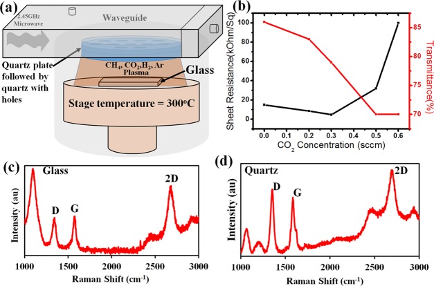
Experiments were performed at different CO2 concentrations along with CH4, H2, and Ar with an initial microwave power of 800 W. It was found that at CO2 concentrations higher than 0.3 standard cubic centimeters (sccm), sheet resistance of the deposited carbon film increased drastically. With respect to sheet resistance and transmittance, 0.3 sccm of CO2 along with CH4, H2, and Ar gave acceptable results. Figure 1b shows that sheet resistance and transmittance of as-deposited substrates varied with CO2 concentration. After spotting the best concentration of CO2, experiments with other microwave powers were performed and 1000 W was found to give acceptable deposition among 700–1200 W microwave powers (please refer to Table S1 in the Supporting Information for a detailed explanation). Synthesized films on glass and quartz were first characterized by Raman spectroscopy. Figure 1c shows a typical Raman spectrum of graphene on a glass surface. Peaks at 1350, 1580, and 2682 cm–1 correspond to D peak, G peak, and 2D peak, respectively, confirming the formation of few-layer graphene on a glass surface. Similarly, the Raman spectrum for quartz shown in Figure 1d also confirms the formation of graphene. The D peak seen in the Raman spectrum can be attributed to defects, such as lattice disorders and unintentional impurity substitutional doping in synthesized graphene lattice.35 It is also observed from previous reports that plasma CVD forms vertically grown carbon walls or diamondlike carbon much easily than lateral graphene growth.36,37 Along with lattice disorders, vertical carbon walls or diamondlike carbon may give rise to defect peaks in the Raman spectrum. A strong D peak is a typical feature of diamondlike carbon because of a nanocrystalline structure and more defects, such as disorders, vacancies, and strains.38 Therefore, to evaluate the morphology of as-synthesized graphene, we performed detailed surface morphology examination using optical imaging, atomic force microscopy (AFM), and scanning electron microscopy (SEM) analyses.
Figure 1.
(a) Schematic of microwave plasma CVD used for direct graphene synthesis, (b) dependence of sheet resistance and transmittance of glass (or quartz) on CO2 concentration used during graphene growth, Raman spectra of (c) glass and (d) quartz surfaces after carbon film deposition using PCVD.
Figure 2a shows the optical image of a quartz surface after graphene growth. From the optical image observed, there is no clear evidence of carbon wall formation. Also the SEM image in Figure 2b captured with the sample inclined by 60° with respect to the horizontal clearly shows an almost smooth surface except for a small hump highlighted by an ellipse indicating that graphene has grown laterally. The AFM analysis shown in Figure 2c,d also confirms that no carbon wall formation occurred, and the line profile (Figure 2e) of the quartz surface indicates that graphene is laterally grown on a quartz substrate with a surface roughness of a few units of nanometers. From surface morphology examinations, it is clear that lateral graphene has been formed; therefore, the D peak in the Raman spectrum might have appeared either by lattice disorders in graphene or the smaller grain size of graphene or defects caused due to high-energy radicals forming plasma.39 Nevertheless, the use of the 0.3 sccm CO2 during the synthesis process has improved sheet resistance and transmittance by a considerable amount. A comparative study between graphene synthesis without and with CO2 has been shown below for a better understanding of CO2 impact on graphene growth. In Figure 3a, a typical cross-sectional SEM image of a silicon sample with graphene deposition without CO2 clearly shows vertically grown structures, whereas in Figure 3b, a cross-sectional SEM image of the sample with CO2 shows that there is no such vertical growth. Figure 3c,d shows the top view optical image of the same graphene samples, revealing differences in surface morphologies of sample surfaces after deposition without and with CO2. The Raman spectrum in Figure 3e shows a higher D peak with G′ and diminished 2D peaks indicating the formation of a graphitic structure with higher defects, disorders, and unintentional structural impurities such as carbon walls, whereas in the case of graphene synthesis with CO2, the Raman spectrum in Figure 3f shows an elevated 2D peak and comparatively diminished D peak.
Figure 2.
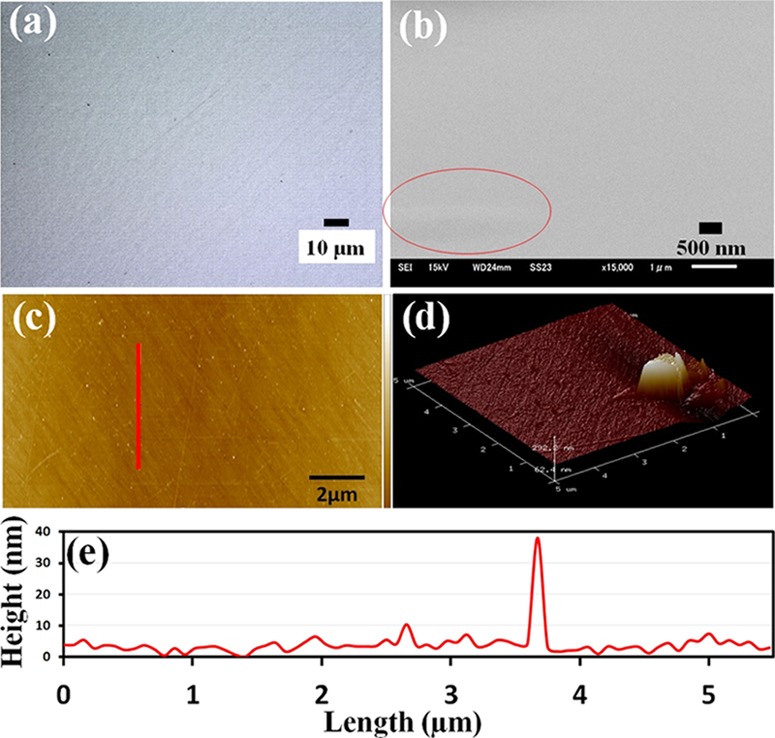
(a) Optical image, (b) cross-sectional SEM image, (c) AFM image, (d) three-dimensional AFM image, and (e) line profile of a graphene/quartz surface.
Figure 3.
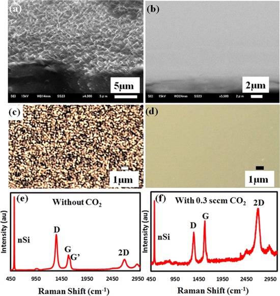
(a, b) Cross-sectional SEM image, (c, d) optical image, (e, f) Raman spectra of a silicon surface after deposition without and with CO2 use in plasma CVD, respectively.
A plasma environment has various factors affecting the growth of graphene, such as different mobilities of electrons or positive ions at different gas compositions, pressure and temperature gradients, microwave power, etc. Also, numerous carbon network formations can be imagined due to infinite bonding possibilities offered by sp3 and sp2 sites. A possible growth mechanism can be as explained on the basis of the hydrogen (H)-shifting reaction. Hydrogen is well known for catalytic activity; H-shifting activates a series forming C2Hx (eqs 1 and 2) in the hot region, which on further H-shifting may lead to the formation of CnHy species.40 Possible reaction equations can be written as follows
| 1 |
| 2 |
| 3 |
| 4 |
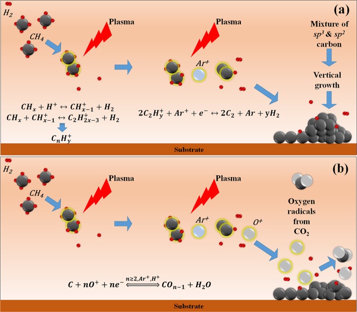
Ar is usually added to enhance the plasma stability. It makes plasma capable of providing electrons of higher energy and the required level of ionization. There are some reports on Ar helping in C2 formation route (eq 3). This, in turn, enhances the degree of graphitization on the substrate. Nevertheless, a higher concentration of C2 may also boost vertical growth or diamondlike structures with prominent D peaks (see also Figure S2), as illustrated in Figure 4a.41 On the other hand, the introduction of a small amount of CO2 is found to yield improved graphene growth. Son et al. in 2016 reported that CO2 helps in graphene growth with lesser defects by etching poor cross-links between growing flakes.42 The etching property of CO2 might help in removal of excess sp3 carbon (eq 4), helping in reduction of vertical growth or diamondlike carbon and, in turn, reducing the defects. With suppressed vertical growth, sp2 bonded C–C chain might dominate to form lateral graphene, as illustrated in Figure 4b. Therefore, introduction of CO2 during the growth process can be useful for lateral graphene growth using plasma CVD with improved sheet resistance and transmittance.
Figure 4.
(a, b) Schematic representation of the graphene growth mechanism without and with CO2 use in plasma CVD, respectively.
To estimate the thickness of graphene, a scratch was made on a continuous graphene/SiO2/Si surface and AFM measurement was performed. Graphene was deposited directly on SiO2/Si especially for AFM analysis to get a clear contrast between the surface and graphene. The contrast on SiO2/Si surface with graphene layers makes it easier to locate the scratch in the optical observation during AFM measurement. Figure 5a shows the AFM image of graphene/SiO2/Si surface with a scratched surface on the left and graphene (yellowish part) on the right side in the image. The figure also confirms lateral graphene growth on SiO2/Si surface complimenting previous explanations. The line profile in Figure 5b confirms the formation of few-layer graphene with a thickness of 1.2 nm on SiO2/Si surface. Figure 5c,d shows a magnified AFM image of the graphene sample, revealing graphene grain size of 50–70 nm. To further investigate the grain size of as-grown graphene and surface morphology, the deposition time was reduced to 2 min and then AFM measurements were performed. The AFM image shown in Figure S5 indicates that the graphene grain size varies from 20–30 nm, suggesting that graphene grains grow in size and overlap each other on increasing the deposition time. Sheet resistance measurements performed using the four-probe technique reveal that graphene has been formed with sheet resistance varying from 2.1 to 2.8 kΩ/□, as shown in Figure 6a and transmittance in Figure 6b from 74 to 80% (both with blue lines). With the above-mentioned growth conditions, few nanometer thick large-area graphene can be synthesized on an insulating substrate at a temperature of 300 °C.
Figure 5.
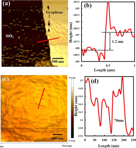
(a) AFM image and (b) line profile of graphene/SiO2 surface; (c) magnified AFM image and (d) the corresponding line profile of the graphene sample.
Figure 6.
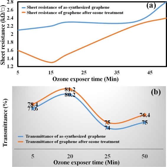
Effect of ozone treatment on (a) sheet resistance and (b) transmittance of PCVD-synthesized graphene.
Directly synthesized graphene on insulating substrates with a sheet resistance of 2.1–2.8 kΩ/□ and transmittance of 74–80% was treated with ozone for various time periods to remove surface contaminations. It is assumed that ozone treatment would cleanse surface contaminations such as amorphous carbon or other surface impurities. There are reports on the ozone treatment of TCVD graphene or exfoliated graphene. However, this is the first report on the ozone treatment of graphene synthesized using microwave plasma CVD without a transfer process. According to a report by Li et al., 10 min of ultraviolet/ozone treatment of transferred graphene synthesized using TCVD is found to enhance metal–graphene contact by removal of surface contaminations. Also, such a short duration exposure of UV/ozone did not introduce disorders in as-synthesized graphene.43Figure 6 shows the change in sheet resistance of graphene after the ozone treatment. It is clear from the figure that graphene exposed in ozone for the time range between 15 and 20 min has better qualities in terms of sheet resistance and transmittance than as-synthesized graphene. The sheet resistance and transmittance of the quartz substrate changed from 2.2 kΩ/□ and 79% to 1.3 kΩ/□ and 80%, respectively, after 15 min of ozone treatment, as shown in Figure 6. Raman mapping has also been performed to understand the quality of graphene on a larger scale. Figure 7a–c shows the Raman spectroscope map of D peak, G peak, and 2D peak intensity, respectively, with baseline correction. Mapping shows formation of graphene in the 20 × 20 μm2 range with some defects. These defects can be attributed to the smaller grain size of graphene and/or defect sites, as mentioned earlier. Figure 8a shows the Raman spectroscope map of normalized G/2D; it can be seen from the map that G peak intensity is higher than 2D peak intensity in most of the areas, indicating formation of few-layer graphene, and from the mapping image of D/G intensities shown in Figure 8b, it is clear that the large-area graphene is formed with varying D peak intensity.
Figure 7.
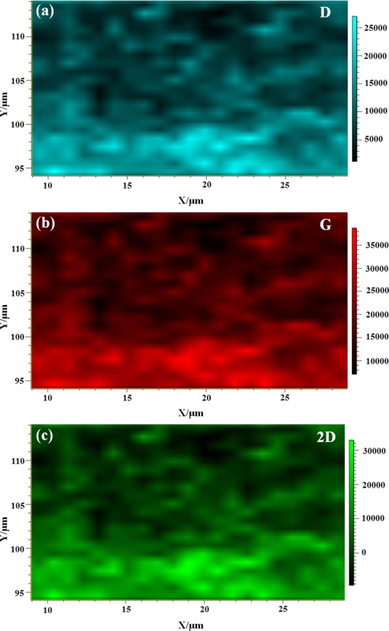
Raman mapping of (a) D peak intensity, (b) G peak intensity, and (c) 2D peak intensity.
Figure 8.
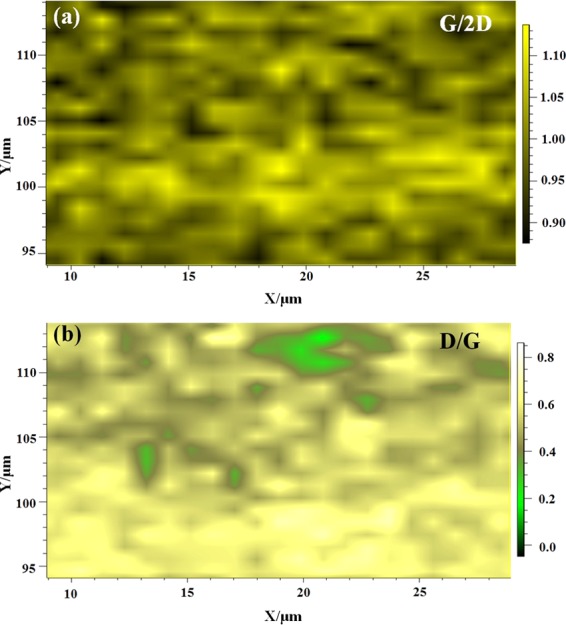
Raman mapping of (a) G/2D peak intensity and (b) D/G peak intensity.
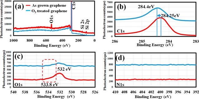
Ozone exposure has improved graphene sheet resistance by 30–35% and transmittance by 1%. To investigate the effect of ozone treatment on graphene, X-ray photoelectron spectroscopy (XPS) analysis was performed on as-grown and ozone-treated graphene samples. Figure 9a shows XPS survey of graphene/quartz surface before and after the ozone treatment, indicating the presence of silicon (Si), carbon (C), and oxygen (O). Figure 9b showing the C 1s spectrum confirms the formation of sp2 carbon with a peak at 284.25 eV assigned to C–C bonding.44 The shift in C 1s peak can be clearly seen in the figure from 284.25 to 284.4 eV after the ozone treatment. This shift of 0.15 eV toward higher binding energy can be attributed to physisorption of ozone molecules on graphene.45 The physisorption binding energy of ozone on the graphene surface is less than 0.3 eV.46 As reported by Jandhyala et al., this physisorbed ozone can be responsible for the upshift of the Dirac point, leading to p-type doping of mechanically exfoliated graphene. With the increase in p-type doping, an improved electrical conductivity can be expected.47 The ozone treatment of graphene for more than 20 min would lead to the formation of epoxide groups on the graphene basal plane due to chemisorption of ozone. This would lead to an increase in surface defects in graphene and thus increase in sheet resistance.48 There are reports on sheet resistance and mobility enhancement using the ozone treatment of exfoliated graphene also, apart from TCVD-grown graphene.49 However, this is the first report of ozone treatment on directly grown graphene using plasma CVD. Table 1 shows the effect of the ozone treatment on sheet carrier mobility and sheet carrier concentration of graphene. Carrier mobility increases up to 97.5 cm2/(V s) after the ozone treatment with a reduction in sheet carrier concentration. The increase in mobility is 43.8% more than the calculated value of mobility, and the decrease in carrier concentration is 56.2% less than the calculated value of carrier concentration in the case when no effect of ozone is assumed (Table S3). These mismatches in carrier mobility and concentration confirm that the ozone treatment has a constructive effect on sheet resistance of graphene. Oxygen, as detected in the O 1s spectrum shown in Figure 9c, might have appeared from either use of CO2 during the synthesis process or quartz surface beneath the graphene film or C–O bond formation. The O 1s spectrum also shows the formation of a hump toward higher binding energy after the ozone treatment. This hump at 533.8 eV can be attributed to Si–O bonding, indicating that the quartz surface is exposed more to X-rays after the ozone treatment. Hump formation in O 1s spectrum confirms that the ozone treatment removes surface contaminations (such as sp3-bonded amorphous carbon) (Figure S4) and forms physisorbed ozone on the graphene surface, which might help in improving sheet carrier mobility and sheet resistance of graphene. Figure 9d confirms that there is no nitrogen in as-grown graphene or after the ozone treatment.
Figure 9.
(a) XPS survey spectrum, (b) C 1s, (c) O 1s, and (d) N 1s spectra for as-grown and ozone-treated graphene.
Table 1. Effect of Ozone Treatment on Carrier Mobility and Carrier Concentration of Graphene.
| carrier mobility (cm2/(V s)) | sheet carrier concentration (/cm2) | sheet resistance (Ω/□) | |
|---|---|---|---|
| before ozone treatment | 9.64 | 2.89 × 10¹⁴ | 2240 |
| after ozone treatment | 97.5 | 5.09 × 10¹³ | 1259 |
Conclusions
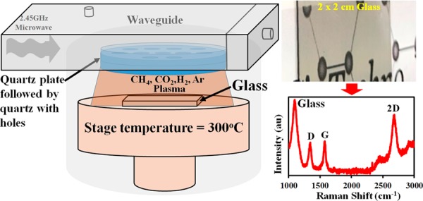
In conclusion, direct graphene growth on a 2 × 2 cm2 insulating substrate has been achieved at a temperature of 300 °C using magnetron-generated plasma CVD. The growth of graphene is controlled by using a small amount of CO2. After further treatment with ozone, graphene with sheet resistance 1.3 kΩ/□ and 80% transmittance is obtained. The ozone treatment is found to clean surface contamination, enhancing transmittance and sheet carrier mobility of graphene. These results can be useful in direct growth of graphene at low temperatures on any insulating substrates, escalating research in the field of predicted industrial application possibilities of graphene.
Experimental Section
Experiments were performed on a 2 × 2 × 0.1 cm3 quartz piece and micro slide glass (procured from Matsunami Glass IND. LTD. Japan) using the plasma CVD (Shinko Seiki, Japan) with a quartz plate followed by another quartz plate having apertures. It has been reported that on using a quartz plate with holes, plasma is generated without any density jump and has a higher density as compared to that using a flat plate. High-density plasma can be generated on a meter-scale, and large-area deposition can be easily achieved using such plasma CVD.34 The schematic representation of the system used for the growth of graphene film is shown in Figure 1a. For deposition of graphene, a gas mixture of methane (CH4), hydrogen (H2), carbon dioxide (CO2), and argon (Ar) with flow rates of 4, 15, 0.3, and 15 sccm (standard cubic centimeters per min), respectively, were chosen for all experiments after optimization. The microwave power of 1000 W having a negligible amount of fluctuation was used. A gas composition pressure of 10 Pa was used for a duration of 4 min for graphene deposition (Figure S2 in the Supporting Information) on a micro slide glass and quartz-sonicated for 15 min in acetone. After deposition, insulating substrates were treated with ozone to further improve the sheet resistance and transmittance of deposited carbon films on glass and quartz. Ozone was produced using a high-voltage supply (9 kV) between stainless steel mesh separated by 8 mm. After deposition, substrates were characterized with Raman spectroscopy with a laser excitation energy of 532 nm using the Renishaw InVia Laser Raman microscope and X-ray photoelectron spectroscopy (XPS) using PHI 5000 VersaProbe. To analyze the surface morphology of the deposited carbon film, optical imaging with a Keyence VHX-6000 optical microscope, scanning electron microscopy (SEM) with JSM-6510, and the Innova atomic force microscope (AFM) Bruker were used. Optical transmittance characterization of the carbon-deposited surfaces was carried out with UV–vis–NIR on a JASCOV570 spectrophotometer. The sheet resistance of carbon film was measured with a four-probe technique (RT-70V-Napson Corporation, Japan). Hall effect measurements were carried out using Lake Shore 8400 Series (Toyo Corporation, Japan) with the van der Pauw technique.
Acknowledgments
This work is supported by New Energy and Industrial Technology Development Organization (NEDO) Japan (Grant No. 17102103-0).
Supporting Information Available
The Supporting Information is available free of charge on the ACS Publications website at DOI: 10.1021/acsomega.9b00988.
Sheet resistance and transmittance of graphene synthesized at different microwave powers; dependence of sheet resistance and transmittance on deposition time; cross-sectional view and top view optical image of glass surface after graphene deposition without CO2, Raman spectrum of deposited graphene; optical transmittance of graphene deposited on quartz; surface composition of graphene-grown quartz surface; Raman spectra of the quartz surface before and after the ozone treatment; AFM image of the quartz surface after graphene deposition for 2 min; effect of the ozone treatment on carrier mobility and carrier concentration of graphene (PDF)
The authors declare no competing financial interest.
Supplementary Material
References
- Novoselov K. S.; Geim A. K.; Morozov S. V.; Jiang D.; Zhang Y.; Dubonos S. V.; Grigorieva I. V.; Firsov A. A. Electric Field Effect in Atomically Thin Carbon Films. Science 2004, 306, 666–669. 10.1126/science.1102896. [DOI] [PubMed] [Google Scholar]
- Chen S.; Wu Q.; Mishra C.; Kang J.; Zhang H.; Cho K.; Cai W.; Balandin A. A.; Ruoff R. S. Thermal Conductivity of Isotopically Modified Graphene. Nat. Mater. 2012, 11, 203–207. 10.1038/nmat3207. [DOI] [PubMed] [Google Scholar]
- Du X.; Skachko I.; Andrei E. Y.; Barker A. Approaching Ballistic Transport in Suspended Graphene. Nat. Nanotechnol. 2008, 3, 491–495. 10.1038/nnano.2008.199. [DOI] [PubMed] [Google Scholar]
- Li N.; Song H.; Cui H.; Wang C. Sn@graphene Grown on Vertically Aligned Graphene for High-Capacity, High-Rate, and Long-Life Lithium Storage. Nano Energy 2014, 3, 102–112. 10.1016/j.nanoen.2013.10.014. [DOI] [Google Scholar]
- Dai L.; Chang D. W.; Baek J.-B.; Lu W. Carbon Nanomaterials for Advanced Energy Conversion and Storage. Small 2012, 8, 1130–1166. 10.1002/smll.201101594. [DOI] [PubMed] [Google Scholar]
- Chen Y.-Z.; Medina H.; Tsai H.-W.; Wang Y.-C.; Yen Y.-T.; Manikandan A.; Chueh Y.-L. Low Temperature Growth of Graphene on Glass by Carbon-Enclosed Chemical Vapor Deposition Process and Its Application as Transparent Electrode. Chem. Mater. 2015, 27, 1646–1655. 10.1021/cm504431d. [DOI] [Google Scholar]
- Zhu Y.; Murali S.; Cai W.; Li X.; Suk J. W.; Potts J. R.; Ruoff R. S. Graphene and Graphene Oxide: Synthesis, Properties, and Applications. Adv. Mater. 2010, 22, 3906–3924. 10.1002/adma.201001068. [DOI] [PubMed] [Google Scholar]
- Geim A.; Novoselov K. Graphene — the Perfect Atomic Lattice, R. Swedish Acad. Sci. 2011, 181, 1283. 10.3367/UFNr.0181.201112d.1283. [DOI] [Google Scholar]
- Novoselov K. S.; Fal’ko V. I.; Colombo L.; Gellert P. R.; Schwab M. G.; Kim K. A Roadmap for Graphene. Nature 2012, 490, 192–200. 10.1038/nature11458. [DOI] [PubMed] [Google Scholar]
- Schwierz F. Graphene Transistors. Nat. Nanotechnol. 2010, 5, 487–496. 10.1038/nnano.2010.89. [DOI] [PubMed] [Google Scholar]
- Naghdi S.; Rhee K. Y.; Park S. J. A Catalytic, Catalyst-Free, and Roll-to-Roll Production of Graphene via Chemical Vapor Deposition: Low Temperature Growth. Carbon 2018, 127, 1–12. 10.1016/j.carbon.2017.10.065. [DOI] [Google Scholar]
- Polsen E. S.; McNerny D. Q.; Viswanath B.; Pattinson S. W.; John Hart A. High-Speed Roll-to-Roll Manufacturing of Graphene Using a Concentric Tube CVD Reactor. Sci. Rep. 2015, 5, 10257 10.1038/srep10257. [DOI] [PMC free article] [PubMed] [Google Scholar]
- Bae S.; Kim H.; Lee Y.; Xu X.; Park J.-S.; Zheng Y.; Balakrishnan J.; Lei T.; Ri Kim H.; Song Y. Il; et al. Roll-to-Roll Production of 30-Inch Graphene Films for Transparent Electrodes. Nat. Nanotechnol. 2010, 5, 574–578. 10.1038/nnano.2010.132. [DOI] [PubMed] [Google Scholar]
- An H.; Lee W. J.; Jung J. Graphene Synthesis on Fe Foil Using Thermal CVD. Curr. Appl. Phys. 2011, 11, S81–S85. 10.1016/j.cap.2011.03.077. [DOI] [Google Scholar]
- Xin H.; Li W. A Review on High Throughput Roll-to-Roll Manufacturing of Chemical Vapor Deposition Graphene. Appl. Phys. Rev. 2018, 5, 031105 10.1063/1.5035295. [DOI] [Google Scholar]
- Kim J.; Park H.; Hannon J. B.; Bedell S. W.; Fogel K.; Sadana D. K.; Dimitrakopoulos C. Layer-Resolved Graphene Transfer via Engineered Strain Layers. Science 2013, 342, 833–836. 10.1126/science.1242988. [DOI] [PubMed] [Google Scholar]
- Matković A.; Ralević U.; Chhikara M.; Jakovljević M. M.; Jovanović D.; Bratina G.; Gajić R. Influence of Transfer Residue on the Optical Properties of Chemical Vapor Deposited Graphene Investigated through Spectroscopic Ellipsometry. J. Appl. Phys. 2013, 114, 093505 10.1063/1.4819967. [DOI] [Google Scholar]
- Park B. J.; Choi J. S.; Eom J. H.; Ha H.; Kim H. Y.; Lee S.; Shin H.; Yoon S. G. Defect-Free Graphene Synthesized Directly at 150 °C via Chemical Vapor Deposition with No Transfer. ACS Nano 2018, 12, 2008–2016. 10.1021/acsnano.8b00015. [DOI] [PubMed] [Google Scholar]
- Song H. J.; Son M.; Park C.; Lim H.; Levendorf M. P.; Tsen A. W.; Park J.; Choi H. C. Large Scale Metal-Free Synthesis of Graphene on Sapphire and Transfer-Free Device Fabrication. Nanoscale 2012, 4, 3050–3054. 10.1039/c2nr30330b. [DOI] [PubMed] [Google Scholar]
- Phillips J. M.; Kwo J.; Thomas G. A.; Carter S. A.; Cava R. J.; Hou S. Y.; Krajewski J. J.; Marshall J. H.; Peck W. F.; Rapkine D. H.; et al. Transparent Conducting Thin Films of GaInO3. Appl. Phys. Lett. 1994, 65, 115–117. 10.1063/1.113052. [DOI] [Google Scholar]
- Ismach A.; Druzgalski C.; Penwell S.; Schwartzberg A.; Zheng M.; Javey A.; Bokor J.; Zhang Y. Direct Chemical Vapor Deposition of Graphene on Dielectric Surfaces. Nano Lett. 2010, 10, 1542–1548. 10.1021/nl9037714. [DOI] [PubMed] [Google Scholar]
- Song I.; Park Y.; Cho H.; Choi H. C. Transfer-Free, Large-Scale Growth of High-Quality Graphene on Insulating Substrate by Physical Contact of Copper Foil. Angew. Chem., Int. Ed. 2018, 57, 15374–15378. 10.1002/anie.201805923. [DOI] [PubMed] [Google Scholar]
- Kobayashi T.; Bando M.; Kimura N.; Shimizu K.; Kadono K.; Umezu N.; Miyahara K.; Hayazaki S.; Nagai S.; Mizuguchi Y.; et al. Production of a 100-m-Long High-Quality Graphene Transparent Conductive Film by Roll-to-Roll Chemical Vapor Deposition and Transfer Process. Appl. Phys. Lett. 2013, 102, 023112 10.1063/1.4776707. [DOI] [Google Scholar]
- Lee C. S.; Shin K. W.; Song H. J.; Park H.; Cho Y.; Im D. H.; Lee H.; Lee J. H.; Won J. Y.; Chung J. G.; et al. Fabrication of Metal/Graphene Hybrid Interconnects by Direct Graphene Growth and Their Integration Properties. Adv. Electron. Mater. 2018, 4, 1700624 10.1002/aelm.201700624. [DOI] [Google Scholar]
- Boyd D. A.; Lin W. H.; Hsu C. C.; Teague M. L.; Chen C. C.; Lo Y. Y.; Chan W. Y.; Su W. B.; Cheng T. C.; Chang C. S.; et al. Single-Step Deposition of High-Mobility Graphene at Reduced Temperatures. Nat. Commun. 2015, 6, 6620 10.1038/ncomms7620. [DOI] [PubMed] [Google Scholar]
- Yamada T.; Ishihara M.; Hasegawa M. Large Area Coating of Graphene at Low Temperature Using a Roll-to-Roll Microwave Plasma Chemical Vapor Deposition. Thin Solid Films 2013, 532, 89–93. 10.1016/j.tsf.2012.12.102. [DOI] [Google Scholar]
- Kalita G.; Wakita K.; Umeno M. Low Temperature Growth of Graphene Film by Microwave Assisted Surface Wave Plasma CVD for Transparent Electrode Application. RSC Adv. 2012, 2, 2815–2820. 10.1039/c2ra00648k. [DOI] [Google Scholar]
- Sun J.; Chen Y.; Cai X.; Ma B.; Chen Z.; Priydarshi M. K.; Chen K.; Gao T.; Song X.; Ji Q.; et al. Direct Low-Temperature Synthesis of Graphene on Various Glasses by Plasma-Enhanced Chemical Vapor Deposition for Versatile, Cost-Effective Electrodes. Nano Res. 2015, 8, 3496–3504. 10.1007/s12274-015-0849-0. [DOI] [Google Scholar]
- Muñoz R.; Martínez L.; López-Elvira E.; Munuera C.; Huttel Y.; García-Hernández M. Direct Synthesis of Graphene on Silicon Oxide by Low Temperature Plasma Enhanced Chemical Vapor Deposition. Nanoscale 2018, 10, 12779–12787. 10.1039/C8NR03210F. [DOI] [PMC free article] [PubMed] [Google Scholar]
- Yamada T.; Ishihara M.; Kim J.; Hasegawa M.; Iijima S. A Roll-to-Roll Microwave Plasma Chemical Vapor Deposition Process for the Production of 294 Mm Width Graphene Films at Low Temperature. Carbon 2012, 50, 2615–2619. 10.1016/j.carbon.2012.02.020. [DOI] [Google Scholar]
- Kim Y. S.; Joo K.; Jerng S. K.; Lee J. H.; Yoon E.; Chun S. H. Direct Growth of Patterned Graphene on SiO2substrates without the Use of Catalysts or Lithography. Nanoscale 2014, 6, 10100–10105. 10.1039/C4NR02001D. [DOI] [PubMed] [Google Scholar]
- Vishwakarma R.; Rosmi M. S.; Takahashi K.; Wakamatsu Y.; Yaakob Y.; Araby M. I.; Kalita G.; Kitazawa M.; Tanemura M. Transfer Free Graphene Growth on SiO2 Substrate at 250 °C. Sci. Rep. 2017, 7, 43756 10.1038/srep43756. [DOI] [PMC free article] [PubMed] [Google Scholar]
- Hirano R.; Matsubara K.; Kalita G.; Hayashi Y.; Tanemura M. Synthesis of Transfer-Free Graphene on an Insulating Substrate Using a Solid Phase Reaction. Nanoscale 2012, 4, 7791–7796. 10.1039/c2nr31723k. [DOI] [PubMed] [Google Scholar]
- Nakao S.; Sugai H. Multi-Hollow Plasma Production along Dielectric Plate in Microwave Discharge. Jpn. J. Appl. Phys. 2007, 46, L1039–L1041. 10.1143/JJAP.46.L1039. [DOI] [Google Scholar]
- Vishwakarma R.; Sharma S.; Shinde S. M.; Kamal P. S.; Thangaraja A.; Kalita G.; Tanemura M. Fabrication of Particular Structures of Hexagonal Boron Nitride and Boron–carbon–nitrogen Layers by Anisotropic Etching. Phys. E 2016, 79, 13–19. 10.1016/j.physe.2015.12.004. [DOI] [Google Scholar]
- Zhao J.; Shaygan M.; Eckert J.; Meyyappan M.; Rümmeli M. H. A Growth Mechanism for Free-Standing Vertical Graphene. Nano Lett. 2014, 14, 3064–3071. 10.1021/nl501039c. [DOI] [PubMed] [Google Scholar]
- Wu Y.; Qiao P.; Chong T.; Shen Z. Carbon Nanowalls Grown by Microwave Plasma Enhanced Chemical Vapor Deposition. Adv. Mater. 2002, 14, 64–67. . [DOI] [Google Scholar]
- Yu J.; Zhang Q.; Ahn J.; Yoon S. F.; Li R. Y. J.; Gan B.; Chew K.; Tan K. H. Synthesis of Carbon Nanostructures by Microwave Plasma Chemical Vapor Deposition and Their Characterization. Mater. Sci. Eng., B 2002, 90, 16–19. 10.1016/S0921-5107(01)00737-1. [DOI] [Google Scholar]
- Lucchese M. M.; Stavale F.; Ferreira E. H. M.; Vilani C.; Moutinho M. V. O.; Capaz R. B.; Achete C. A.; Jorio A. Quantifying Ion-Induced Defects and Raman Relaxation Length in Graphene. Carbon 2010, 48, 1592–1597. 10.1016/j.carbon.2009.12.057. [DOI] [Google Scholar]
- Angus J. C.; Wang Y.; Sunkara M. Metastable Growth of Diamond and Diamond-Like Phases. Annu. Rev. Mater. Sci. 1991, 21, 221–248. 10.1146/annurev.ms.21.080191.001253. [DOI] [Google Scholar]
- Bo Z.; Yang Y.; Chen J.; Yu K.; Yan J.; Cen K. Plasma-Enhanced Chemical Vapor Deposition Synthesis of Vertically Oriented Graphene Nanosheets. Nanoscale 2013, 5, 5180–5204. 10.1039/c3nr33449j. [DOI] [PubMed] [Google Scholar]
- Son I. H.; Park J. H.; Kwon S.; Choi J. W.; Rümmeli M. H. Graphene Coating of Silicon Nanoparticles with CO2-Enhanced Chemical Vapor Deposition. Small 2016, 12, 658–667. 10.1002/smll.201502880. [DOI] [PubMed] [Google Scholar]
- Li W.; Liang Y.; Yu D.; Peng L.; Pernstich K. P.; Shen T.; Hight Walker A. R.; Cheng G.; Hacker C. A.; Richter C. A.; et al. Ultraviolet/Ozone Treatment to Reduce Metal-Graphene Contact Resistance. Appl. Phys. Lett. 2013, 102, 183110 10.1063/1.4804643. [DOI] [Google Scholar]
- Pirkle A.; Chan J.; Venugopal A.; Hinojos D.; Magnuson C. W.; McDonnell S.; Colombo L.; Vogel E. M.; Ruoff R. S.; Wallace R. M. The Effect of Chemical Residues on the Physical and Electrical Properties of Chemical Vapor Deposited Graphene Transferred to SiO2. Appl. Phys. Lett. 2011, 99, 122108 10.1063/1.3643444. [DOI] [Google Scholar]
- Prudkovskiy V. S.; Katin K. P.; Maslov M. M.; Puech P.; Yakimova R.; Deligeorgis G. Efficient Cleaning of Graphene from Residual Lithographic Polymers by Ozone Treatment. Carbon 2016, 109, 221–226. 10.1016/j.carbon.2016.08.013. [DOI] [Google Scholar]
- Lee G.; Lee B.; Kim J.; Cho K. Ozone Adsorption on Graphene: Ab Initio Study and Experimental Validation. J. Phys. Chem. C 2009, 113, 14225–14229. 10.1021/jp904321n. [DOI] [Google Scholar]
- Jandhyala S.; Mordi G.; Lee B.; Lee G.; Floresca C.; Cha P.; Ahn J.; Wallace R. M.; Chabal Y. J.; Kim M. J.; et al. Atomic Layer Deposition of Dielectrics on Graphene Using Reversibly Physisorbed Ozone. ACS Nano 2012, 6, 2722–2730. 10.1021/nn300167t. [DOI] [PubMed] [Google Scholar]
- Leconte N.; Moser J.; Ordejo P.; Tao H.; Bachtold A.; Roche S.; et al. Damaging Graphene with Ozone Treatment: A Chemically Tunable Metal–Insulator Transition. ACS Nano 2010, 4, 4033–4038. 10.1021/nn100537z. [DOI] [PubMed] [Google Scholar]
- Yang H.; Qin S.; Peng G.; Zheng X.; Zhang X. Ultraviolet-Ozone Treatment for Effectively Removing Adhesive Residue on Graphene. Nano 2016, 11, 1650141 10.1142/S1793292016501411. [DOI] [Google Scholar]
Associated Data
This section collects any data citations, data availability statements, or supplementary materials included in this article.


