Abstract
This paper presents a mm-sized, free-floating, wirelessly-powered, implantable optical stimulation (FF-WIOS) device for untethered optogenetic neuromodulation. A resonator-based 3-coil inductive link creates a homogeneous magnetic field that continuously delivers sufficient power (>2.7 mW) at an optimal carrier frequency of 60 MHz to the FF-WIOS in the near field without surpassing the specific absorption rate (SAR) limit, regardless of the position of the FF-WIOS in a large brain area. Forward data telemetry carries stimulation parameters by on-off-keying (OOK) the power carrier at a data rate of 50 kbps to selectively activate a 4×4 μLED array. Load-shift-keying (LSK) back telemetry controls the wireless power transmission (WPT) by reporting the FF-WIOS received power level in a closed-loop power control (CLPC) mechanism. LEDs typically require high instantaneous power to emit sufficient light for optical stimulation. Thus, a switched-capacitor based stimulation (SCS) architecture is used as an energy storage buffer with one off-chip capacitor to receive charge directly from the inductive link and deliver it to the selected μLED at the onset of stimulation. The FF-WIOS system-on-a-chip (SoC) prototype, fabricated in a 0.35-μm standard CMOS process, charges a 10 μF capacitor up to 5 V with 37% efficiency and passes instantaneous current spikes up to 10 mA in the selected μLED, creating a bright exponentially decaying flash with minimal wasted power. An in vivo experiment was conducted to verify the efficacy of the FF-WIOS by observing light-evoked local field potentials (LFP) and immunostained tissue response from the primary visual cortex (V1) of two anesthetized rats.
Keywords: Optogenetic switched-capacitor based stimulation, mm-sized, free-floating, implantable, inductive link, μLED array
I. Introduction
OPTOGENETICS is becoming popular as an important technique in neuro-science. This technique activates or inhibits genetically-modified neurons that express light-sensitive opsin proteins, using light at certain wavelengths [1]-[4]. In comparison with traditional electrical stimulation, optical stimulation has several advantages, which include cell-type specificity, millisecond temporal precision, and rapid reversibility [1]-[4]. Therefore, optical stimulation has been widely utilized for brain research, particularly brain mapping, and expected to find clinical applications in various brain disorders that do not respond to medication, such as Parkinson’s disease, epilepsy, psychological disorders, and even used in other organs, such as cardiac electrophysiology [4].
Laser is commonly used in optogenetic experiments, but it requires optical fiber or waveguide connectivity to deliver light from an external source to the target tissue [5]-[8]. The tethering effect, however, may bias the natural behavior of the animal subjects. It is not feasible in animal studies that involve multiple subjects either or those that are conducted in specific environments, such as tunnels [4]. LEDs have much smaller size, and can be directly integrated in the optical devices that are small enough to be carried by the animal subjects [9]-[15]. LED-based devices, whether in the form of detachable headstage or implant, eliminate the tethering effect of a stationary light source, facilitating in vivo experiments on freely behaving subjects [10]-[15]. The implantable module, under control of the external headstage, is implemented as a probe with integrated LEDs, penetrating deep into the brain or placed on the brain surface [10]-[13]. In some cases, optical fibers are used to guide the light from LEDs embedded in the headstage to the target brain area [14], [15]. However, the transcutaneous connection between the headstage and implantable module could cause infection and damage to the surrounding soft tissue, which may not be a major concern in animal studies but a key concern in translation towards a clinical solution [16]. To prevent physical trauma of the transcutaneous connection, miniature implants are expected to minimize tissue damage by reducing foreign body reaction [16].
Recently, a few wirelessly-powered optogenetics approaches have been reported, demonstrating significant reduction in the implant size [17]-[21]. In [17], [18] the proposed optical stimulators, equipped with the energy-harvesting unit, either a coil [17] or a stretchable antenna on board [18], are wirelessly powered in the GHz band. The specific absorption rate (SAR) of electromagnetic (EM) field in the tissue, which mainly consists of water, at high frequencies is rather high [22]. Moreover, operation in these bands produces considerable radiation, which results in interference with other laboratory instruments or wireless devices in the environment [23].
To circumvent the challenges associated with wireless operation in GHz bands, the carrier frequency in [19] is limited to 13.56 MHz. However, in this case, the receiver (Rx) coil with a diameter of 9.8 mm becomes the main limiting factor in the device miniaturization. A photovoltaic power transfer strategy is proposed in [20] to wirelessly power the implant using infrared (IR) light. In this case, the overall power transfer efficiency (PTE) is quite low, and additional post-processing steps, needed in microfabrication of the silicon die and separation of the photovoltaic cells, could reduce the yield. In [21]. an ultrasonically-powered mm-sized implant enables both optical and electrical stimulations, at the cost of increasing size and weight of the external transmitter, which is too large to be carried by a behaving animal subject. Moreover, even though ultrasonic power transmission is immune to EM interference and offers good PTE in deeper tissues, it is quite sensitive to transducer misalignments and cannot penetrate bone/skull.
In this paper, we are demonstrating a mm-sized, free-floating, wirelessly-powered, implantable optical stimulation (FF-WIOS) device, building upon our preliminary results in [24]-[26], to address the abovementioned limitations. System functionality has been validated in vivo on anesthetized rats by observing light-evoked local field potentials (LFPs) and immunostained tissue response. The miniaturized version of the FF-WIOS device is built on polyimide substrate, which is verified in vitro. It is an important step towards the free-floating distributed neural interface concept. The main novelties can be summarized as 1) ensuring sufficient and constant power delivered to the load (PDL) at high PTE with the closed-loop power control (CLPC) mechanism, while staying well below the SAR limit, 2) assembling the FF-WIOS device with compact size and light weight, 3) designing the FF-WIOS system-on-a-chip (SoC) with high-level integration of front-end circuits and wireless power/data transmission related circuits for 16-ch wireless optical stimulation, 4) allowing end-users to configure the optical stimulation pattern, e.g. current level, frequency, and pulse width, and selectively turn on/off a μLED of a 4×4 μLED array. An overview of the system is given in Section II. Section III presents the detailed design of the FFWIOS SoC. Section IV describes the 3-coil inductive link specifically designed for this particular application. Section V discusses the benchtop measurement, in vitro, and in vivo results, followed by concluding remarks.
II. System Architecture
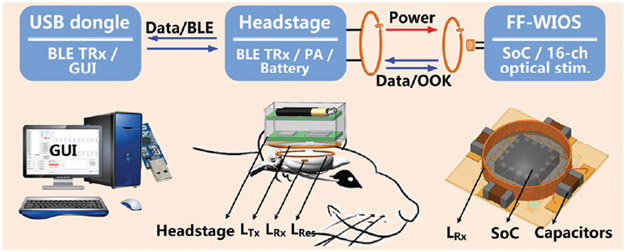
The conceptual view of the system that wirelessly powers and controls the mm-sized FF-WIOS is shown in Fig. 1. The FF-WIOS, which includes a SoC, surface-mount device (SMD) capacitors (0201), Rx coil, and μLEDs, all mechanically supported on a 100 μm-thick polyimide substrate, and hermetically sealed with Parylene-C and polydimethylsiloxane (PDMS) for acute testing, is designed to be implanted on the surface of the subject’s brain. The wire-wound Rx coil, LRx, which encompasses the SoC, forms a 3-coil inductive link with a transmitter (Tx) coil, LTx, which is part of the external headstage, and a passive high quality (Q)-factor resonator, LRes, which encompasses one or more FF-WIOS implants roughly in the same plane. The headstage includes a class-E power amplifier (PA), controlled by a microcontroller (MCU) (CC2541, Texas Instruments), which delivers power from battery to the FF-WIOS through the 3-coil link at 60 MHz. To wirelessly control the FF-WIOS, stimulation parameters, which are set in a graphical user interface (GUI) running on a nearby PC, are sent to the headstage MCU via Bluetooth Low Energy (BLE), and then relayed to the FF-WIOS through the 3-coil link by on-off-keying (OOK) the power carrier signal. The rectified voltage on the FF-WIOS is also digitized, as a measure of the received power on the SoC, and sent back to the headstage via load-shift-keying (LSK) to close the power control loop, and eventually send to the PC via BLE for real-time display.
Fig. 1.
A simplified conceptual representation of the free-floating, wirelessly-powered, implantable optical stimulation (FF-WIOS) device being wirelessly powered and controlled by a battery-powered headstage, which is in turn controlled via Bluetooth Low Energy (BLE) by a PC running the GUI.
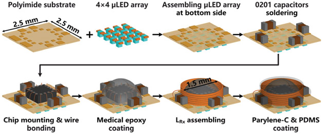
Fig. 2 depicts the steps for microassembly of the FF-WIOS. In the current prototype, 18 μm of copper is patterned on both sides of the polyimide substrate with the diameter of 2.5×2.5 mm2 to form interconnections between the wire-bonded SoC die, μLED pads, and SMD caps. The μLEDs (220×270×50 μm3, TR2227TM, Cree) were mounted on their pads using low melting point solder (144 Alloy Field’s Metal) and then encapsulated using Parylene-C [9], [10]. The μLEDs are separated by 700 μm to ensure enough illumination field distinction. The FF-WIOS SoC was fixated in the center of the substrate for wire bonding, following which it was protected with ultraviolet-cured medical grade epoxy, while capacitors were mounted on the periphery of the SoC die using silver conductive epoxy (MG Chemicals 8331). The wire-wound Rx coil was then mounted around the SoC die and its terminals were connected to one of the SMD capacitors by silver conductive epoxy to form the LRxCRx-tank, resonating at the power carrier frequency. Finally, the FF-WIOS device is sealed with Parylene-C and PDMS.
Fig. 2.
The fabrication and micro-assembly process of the FF-WIOS device.
III. FF-WIOS SoC Design
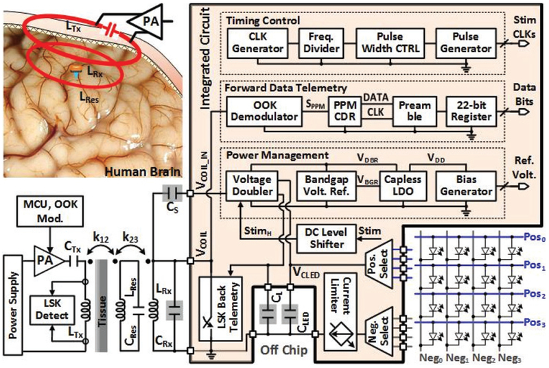
The overall block diagram of the FF-WIOS SoC is shown in Fig. 3. Major challenges in the design of FF-WIOS circuitry include small input power from LRx due to its weak couplings with LTx and LRes, and safety limit on the SAR [22]. On the other hand, instantaneous output power to μLEDs needs to be large enough for the resulting light intensity to surpass the optogenetic stimulation threshold [27]. High efficiency should also be maintained at every step from the PA to the μLED array to minimize heat generation. To address the issues, we adopted the wireless switched-capacitor based stimulation (SCS) circuit in [28]. and modified it for this particular application.
Fig. 3.
A simplified system architecture of the FF-WIOS SoC.
A built-in charger of a voltage double periodically charges a storage capacitor, CLED, from the inductive link. A charge control unit sets the target charging voltage at 5 V. During stimulation, CLED is detached from the charging cell and delivers its stored charge to the selected μLED through positive and negative terminal selector multiplexers without loading the inductive link. A current limiter is added to limit the maximum current flowing through the target μLED. To control the timing of CLED charging/discharging, a timing control block is designed based on the Schmitt trigger in [29] and utilized for generating reference clocks, CLKs, and a stimulation enable signal, Stim, which pulse width and frequency are adjustable [25]. In the power management, the voltage doubler, following LRxCRx-tank, generates a DC voltage, VDBR. A bandgap reference generator uses a classic topology to generate VBGR [29], which is used by a cap-less low dropout regulator (LDO) to generate the supply voltage, VDD. The bias generator block also uses the same VBGR to generate other reference voltages and currents. ADC level shifter shifts the high level voltage of Stim from VDD to VDBR, resulting in a control signal, StimH, for enabling/disabling the built-in charger of the voltage doubler. In the forward data telemetry, a pulse-position-modulated clock/data recovery (PPM-CDR) circuit recovers synchronized clock/data from the OOK modulated coil voltage, VCOIL, setting a 12-bit shift register through a serial-to-parallel (S2P) converter with 10-bit pre/post-amble data [25], [28]. LSK back telemetry is adopted for CLPC of the FF-WIOS by sensing VDBR [28], [30].
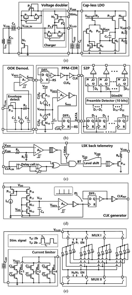
The 60 MHz power carrier induces a VCOIL across the LRxCRx-tank, which is rectified and regulated by the voltage doubler and cap-less low dropout regulator (LDO) blocks, respectively, as shown in Fig. 4a. The built-in charger is controlled by the Stim input, which turns P4 on and N2 off when it is lowered. During stimulation, Stim = ‘1’, the charger is disabled to avoid VDD drop, while CLED is connected to the stimulation sites as shown in Fig. 4e. We adopt dynamic body biasing with two pairs of auxiliary transistors, automatically connecting the body voltage of P1 and P5 to the highest potential [28]. To reduce the number of off-chip components, a cap-less LDO is utilized to generate a stabilized VDD = 1.8 V for the rest of SoC.
Fig. 4.
Schematic diagrams of the (a) voltage doubler with built-in charger and the cap-less LDO, (b) forward data telemetry with OOK modulation, (c) LSK back telemetry, (d) clock generator for the timing of stimulation and charging, (e) current limiter and stimulation output stage.
Fig. 4b shows the schematic diagram of the OOK-based forward data telemetry block, adopted from [28]. In the OOK demodulator, VCOIL is low-pass filtered by an envelope detector, following which OOK pulses are recovered by a hysteresis comparator, A1, when compared with VREF2, to provide the PPM signal, SPPM. In the PPM-CDR block, SPPM is converted to clock, CLK, using a frequency divider. CLK controls the charging and discharging of C3, which generates a triangular waveform, VPPM. If positioning ratio among three consecutive SPPM pulses is 4:1, VPPM exceeds VREF3 during CLK = ‘1’, leading to DATA = ‘1’. Otherwise, DATA = ‘0’, if the positioning ratio is 1:4. In the S2P, the recovered data, DATA, is shifted by CLK into a buffer. Once the pre/post-amble data bits (D1 ~ D5, D18 ~ D22) are matched with a pre-defined 10-bit value, a flag, StimEN, will be raised and then the data bits (D6 ~ D17) will be saved in registers to set the stimulation parameters.
LSK back telemetry is adopted for CLPC of the FF-WIOS. This is a key mechanism for practical implementation in the face of headstage (basically LTx) and brain motion artifacts, as well as uneven brain surface morphology, e.g. gyri and sulci, in larger species. Considering requirements for the CLPC stability in [31]-[34], we have chosen a 160 Hz clock, CLKLSK, to control the timing of back telemetry pulse, BT, which results in a BT data rate of 160 bps. In Fig. 4c, the pulse width of BT (1 μs or 2 μs) is decided by the number of delay cells that are engaged in generating this pulse. The resistive divider, R4 and R5, sets the maximum VDBR at 4.2 V. When the divided VDBR exceeds the bandgap reference voltage, VBGR, BT pulses are generated to short LRx by closing P14 switch, resulting in increasing LRx Q-factor, as well as the voltage across and current through LTx.
Fig. 4d shows the schematic diagram of the clock generator for the timing of charging and stimulation. A control signal, PL, at the output of a hysteresis comparator, A4, controls the timing and amplitude of VC4 by charging C4 in the phase of PL = ‘0’. Once VC4 reaches VREF4, PL is set to ‘ 1 ‘ to discharge C4 in a short period, generating a single narrow PL, which is converted to a reference clock, CLKREF, through a frequency divider. In Fig. 4e, a μLED is selected from the 4×4 μLED array by specifying the positive/negative terminals of the μLED through a pair of 4:1 multiplexers. The current limiter, consisting of a 3-bit programmable current sink with binary-weighted transistors, can adjust the maximum current limit and the light output of the activated μLED. The current sink is controlled by 3 pairs of digital control signals, CL0-CL2 and .
IV. 3-coil Inductive Link Design and Optimization
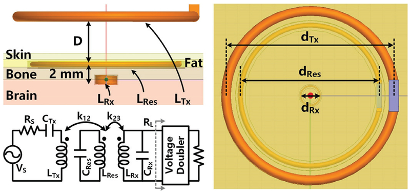
A 3-coil inductive link model with surrounding tissue layers of a rodent model was constructed in HFSS (ANSYS, Cecil Township, PA) for the coil optimization. In Fig. 5, LTX is placed above the head, while LRes and LRX are implanted above and under the skull, respectively. Using a high Q-factor LRes can significantly improve and homogenize the EM field over the area encompassed by LRes. To complete the HFSS model, LRes and LRX are coated with 50 μm PDMS and 5 μm Parylene-C for bio-compatibility. A simplified equivalent circuit model of the inductive link is shown in Fig. 5 as well.
Fig. 5.
The model of the 3-coil inductive link with tissue layers in HFSS and the circuit equivalent model.
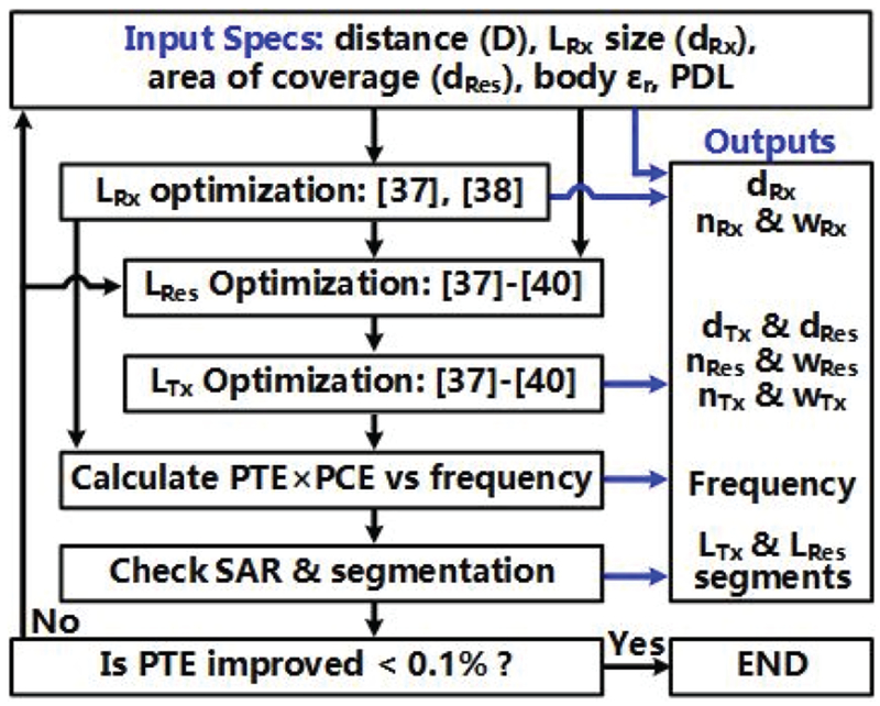
The power conversion efficiency (PCE) of passive AC-DC converters, such as rectifiers and voltage doublers, which use diode-connected transistors, degrades at higher frequencies due to the parasitic capacitance [35], [36]. Considering the effects of surrounding tissue and PCE of the voltage doubler that loads LRx [37]-[40], Fig. 6 shows an algorithm, which generates the optimized coil specifications and operating frequency that would maximize PTE×PCE. Because PTE is obtained by taking into account the loading effect of the voltage doubler, which is reflected through the PCE, it is fine to simply multiply PTE and PCE at each frequency. Other considerations are the application and fabrication constraints, which are the input parameters to the algorithm, including the distance between LTx and LRes, D, LRx diameter, dRx. dRx, LRes diameter, dRes, and PDL. The equivalent load, RL, was set to 4.6 kΩ based on a maximum PDL of 2.7 mW at 5 Vpeak across LRx, which is imposed by the process.
Fig. 6.
The flowchart of algorithm for the 3-coil inductive link optimization.
Design procedure starts with LRx optimization, which effective area is maximized to increase the magnetic flux passing through it. LRx is wire wound around the FF-WIOS die to achieve the highest Q-factor without considerably increasing the diameter of the FF-WIOS. AWG 34 magnet wire is chosen for this purpose, resulting in dRx of 1.6 mm and wire thickness, wRx, of 0.16 mm. The number of turns, nRx, is then fine-tuned for maximizing the receiver power reception susceptibility, Rx-PRS, which indicates the efficiency of LRx power reception under a given magnetic field exposure [37], [38]. To determine nRx, we need to strike a balance between Rx-PRS and geometrical parameters of LTx and LRes as a function of frequency to maximize PTE. Therefore, nRx is chosen after determining the carrier frequency of the 3-coil inductive link
LRes is designed based on the size of the target cortical area. In our application, we expect to observe light-evoked neural activities from the primary visual cortex (V1) of a rat following the FF-WIOS optical stimulation. According to [41], approximately 0.5-5 mm lateral of skull midline overlays V1 in one side lobe. As a result, dRes, should be larger than 10 mm to encompass the V1 areas in both left and right lobes. With a certain margin of error, LRes is implemented with dRes = 11.6 mm. The wire thickness, wRes, and the number of turns, nRes, were selected considering the limited space on the rat skull for LRes, its Q-factor, and coupling coefficient between LRes and LRx. The result was a single-turn coil made of 0.4 mm (AWG 26) magnet wire.
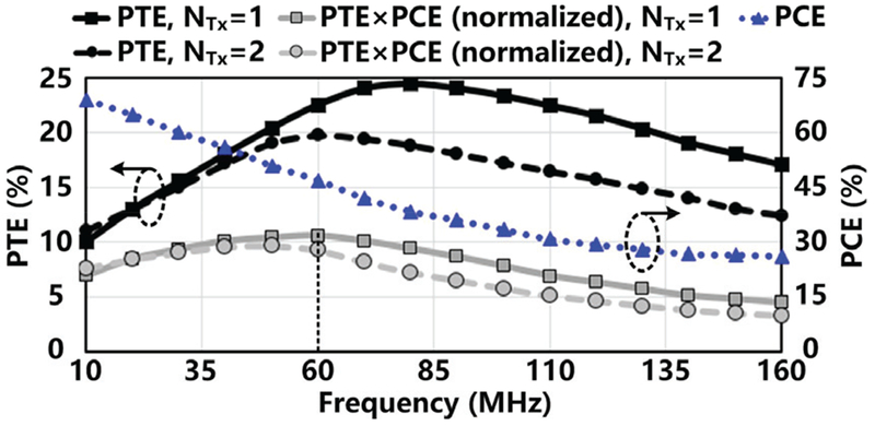
The distance between LTx and LRes, D is determined by the thickness of various tissue layers, depending on the anatomical position of the FF-WIOS. For the rodent model, we considered the thickness of skin and fat to be 5 mm at most. The optimal size of LTx is directly related to D and is calculated for maximum coupling between LTx and LRes using equation (4) in [38]. LTx is made of 0.8 mm (AWG 20) magnet wire for high Q-factor. It is relatively easier to fine-tune LTx parameters compared to those of LRx and LRes. To find the best the number of turns, nTx, PTE of the 3-coil link is simulated from 10 MHz to 160 MHz for 1-and 2-turn LTx in Fig. 7. The PTE with 2-turnLTx is lower across the entire frequency range, and its peak occurs at lower frequency. As a result, LTx is designed as a single-turn coil.
Fig. 7.
HFSS simulation results for PTE of the 3-coil inductive link vs. power carrier frequency and nTx, simulated PCE of the voltage doubler as a function of frequency, and normalized PTE×PCE vs. frequency and nTx.
The PCE of the voltage doubler is yet another key factor in determining the overall efficiency of the power delivery path. In Fig. 7, the PCE of the voltage doubler drops sharply as the frequency increases because of parasitic capacitors of the diode-connected transistors. The best operating frequency was decided based on the peak value of PTE×PCE. The results of PTE×PCE with both 1-turn and 2-turn LTx are divided by the peak value of PTE×PCE for normalization. The peak value of the normalized PTE×PCE appears at 60 MHz with the 1-turn LTx. Thus, 60 MHz is selected as the carrier frequency of the 3-coil inductive link, with nRx = 6.
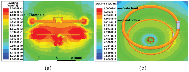
Fig. 8a shows the directional power flux density, i.e. the rate of power transfer per unit area, using Poynting vectors. The power density varies from 1 to 5×l03 W/m2 when the input power level is set at 12.86 mW to deliver a target PDL of ~2.7 mW to the FF-WIOS. The threshold marked on the vertical column indicates the required power flux density to deliver PDL ≥ 2.7 mW. The area where LRx is to be located is above the threshold, indicating sufficient received power. LRes and LRx are concentrically aligned with LTx in this model. In terms of PTE vs. horizontal misalignment, this arrangement is considered the worst-case scenario for LRx, as demonstrated in [38]. Since the 3-coil inductive link provides sufficient PDL in the worst-case scenario, and the Poynting vector in Fig. 8a shows higher EM power density close to the perimeter of LRes, the entire area within LRes is indeed covered with sufficient PDL. Concerning the exposure to EM field and heat generation in the tissue, Fig. 8b presents the HFSS simulation of the local SAR for different tissue layers under the same power source setting. Simulation results show that the maximum local SAR is ~2.78 W/kg, which is well below the safety limit of 20 W/kg [22].
Fig. 8.
(a) Poynting vector and (b) local SAR simulations in HFSS.
V. Experimental results
A. 3-Coil Inductive Link Implementation
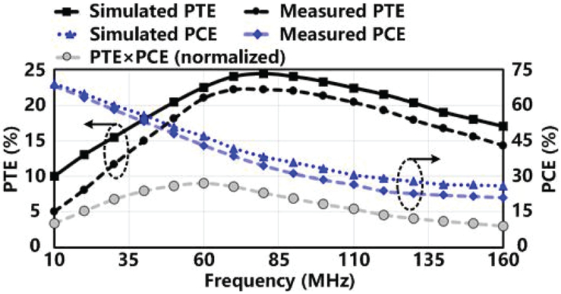
A 3-coil inductive link was implemented using the optimized geometries from Section IV. The PTE of the inductive link and the PCE of the voltage doubler were measured, respectively, and compared with simulations in Fig. 9, as a function of frequency. The PTE×PCE was also calculated, normalized, and added in Fig. 9. Measurements have good agreement with simulation results. The lower PTE in measurements can be attributed to the tissue effect on LRes. Its high Q-factor is affected by the large contact area with the surrounding tissue and makes it sensitive to detuning. The difference between the measured and simulated PCEs could be due to process variation and parasitic effects of the measurement instruments. The parasitic inductance and capacitance from the probes cause distortion in the measured waveforms at higher frequencies, resulting in further reduction in the measured PCE. The key point here is that the optimal carrier frequency to achieve maximum PTE×PCE is still at 60 MHz, as expected from simulations and design target. After fine tuning the optimal inductive link parameters in vitro using fresh tissue from sheep head, they were determined and summarized in Table I.
Fig. 9.
PTE of the 3-coil inductive link and PCE of the voltage doubler in both simulation and measurement as a function of frequency, and normalized PTE×PCE based on the measurement results.
Table I.
Measurement of 3-Coil, Inductive Link Specifications at 60 MHz
| Coil | Tx | Resonator | Rx |
|---|---|---|---|
| Inductance (nH) | 26 | 21.2 | 50.1 |
| Resistance (Ω) | 0.04 | 0.1 | 0.85 |
| Quality factor (Q) | 246 | 79 | 22 |
| Diameter (mm) | 14.3 | 11.6 | 1.6 |
| Number of turns | 1 | 1 | 6 |
| Wire gauge | AWG 20 | AWG 26 | AWG 34 |
| Separation (mm) | DTx-Res = 5 DRes-Rx = 2 | ||
| PTE | 21% | ||
| Carrier frequency (f) | 60 MHz | ||
B. Bench-top Characterization
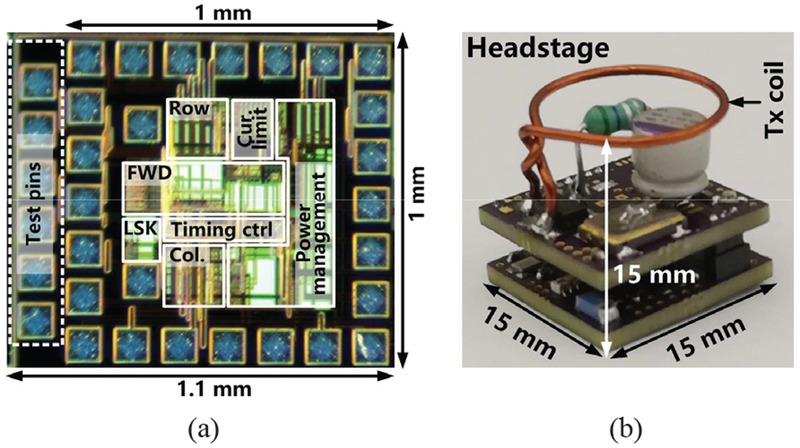
The FF-WIOS SoC was fabricated in the TSMC 0.35-μm 4M2P standard CMOS process, occupying a 1 × 1 mm2 footprint including pads, as shown in Fig. 10a. With additional test pins, the die area is 1.1×1 mm2. Fig. 10b shows a prototype headstage, which consists of two stacked PCBs, together with LTx, fitting in a 15×15×15 mm3 cube. The headstage, made of commercial off-the-shelf (COTS) components, not only drives LTx by its PA but also operates the CLPC [42]. The envelop detector block in the headstage, which has been explained in [42], is used to recover the BT pulses. The resulting signal is then detected by the headstage MCU. Similar to [31], [32], the headstage decreases the PA supply voltage, VPA, when it detects the BT pulses. Otherwise, VPA is continually increased by default at an adjustable rate. In steady state, VPA bounces within a range to stabilize VDBR. The CC2541 MCU applies an upper bound to VPA to avoid any sudden increase.
Fig. 10.
(a) The micrograph of the FF-WIOS SoC and (b) implementation of the prototype headstage with the Tx coil.
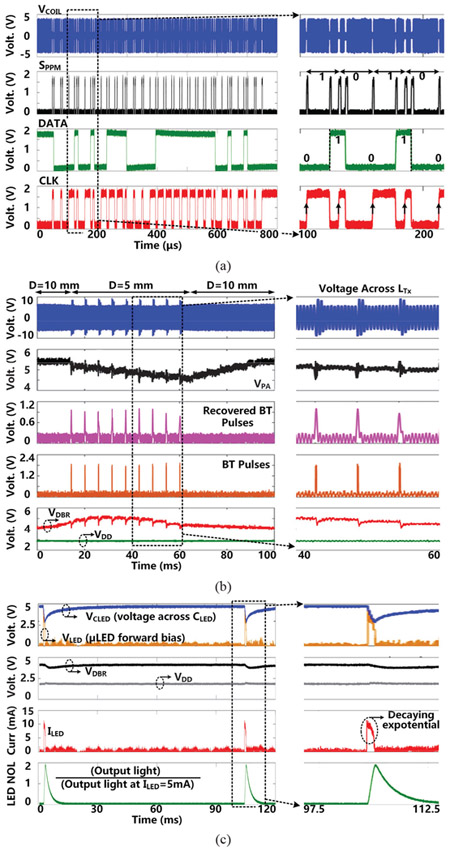
Fig. 11a shows the measurement results of the forward data telemetry. VCOIL is OOK-demodulated to generate SPPM, which is converted to synchronized 50 kbps CLK and DATA by PPM-CDR. In the close-up view, SPPM with pulse position ratio of 4:1 generates DATA = ‘1 ’. On the contrary, when the positioning ratio is 1:4, DATA = ‘O’.
Fig. 11.
Measured results of (a) forward data telemetry, (b) back telemetry for CLPC, and (c) charging and stimulation.
Fig. 11b shows the CLPC operation when the headstage is moved manually from D = 10 mm to 5 mm and then back to 10 mm. As the headstage gets closer to the FF-WIOS, BT pulses are generated when VDBR is larger than a certain threshold, indicating that there is more than enough power available to the FF-WIOS. In response, voltage across LTx increases, and the CLPC starts reducing VPA to compensate for this perturbation. VPA decreases by 1 V in 8 steps, resulting in the step size of 0.125 V. It takes ~60 ms for VDBR to return back to 4.2 V. As the headstage moves back to its original location, VPA starts to increase in the absence of BT pulses. During the short switching period of LRx, the FF-WIOS SoC is powered by the stored charge in CL, and VDD remains stable at 1.8 V.
Fig. 11c shows the charging and discharging of the 10 μF CLED to generate optical stimulation with 2 ms pulse width at 10 Hz. The μLED current. ILED is limited to 10 mA. Once stimulation starts, CLED discharges in the target μLED with a decaying exponential current. VDBR shows a slight drop (0.45 V), which is much less than VCLED (voltage across CLED), and remains above the minimum level (2.6 V) required for VDD not to be affected by its variations. The emitted light from μLED (0.5 × 1×0.4 mm3, LB QH9G, OSRAM) during stimulation pulse was collected by the photodetector (Newport 883-SL) of an optical power meter (Newport 1835-C). The normalized output light (NOL) expectedly follows the stimulation current variation but with a slight delay. After each stimulation, CLED is recharged back to the target voltage within 30 ms.
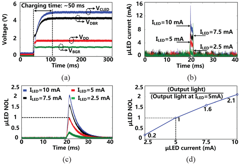
Following startup, as shown in Fig. 12a, it takes ~50 ms for VDBR and VCLED to stabilize at their steady-state target voltages. Before this, VDD and VBGR have already been stabilized within 20 μs at 1.8 V and 1.2 V, respectively. The μLED current under 4 different settings was measured from the voltage across a 10 Ω current-sensing resistor in series with the μLED. In Fig. 12b, ILED increases from 2.5 mA to 10 mA in a 2.5 mA step according to the design specifications. The μLED output light during a stimulation pulse is also measured at each current level with 2 ms pulse width at 10 Hz, as shown in Fig. 12c. To validate measurement results with the μLED datasheet, we normalized the output light. The output light at each μLED current is divided by the peak value of the light intensity (4.8 mW/mm2) under 5 mA current for normalization. Fig. 12d shows that normalized output light intensities under different currents match with specifications of the μLED [43]. A summary of the FF-WIOS SoC characterizations is presented in Table II.
Fig. 12.
(a) Starting up transients of the power management block, (b) measured μLED current at 4 stimulation current settings, and normalized output light as a function of (c) time and (d) μLED current.
Table II.
Measurement of FF-WIOS SoC Specifications
| Overall system | |
|---|---|
| ASIC area | 1 mm2 |
| Power with stimulation | 1 mW (Average) |
| Power without stimulation | 300 μW |
| Voltage doubler efficiency | 43 % |
| Switch capacitor-based stimulation | |
| Target voltage | 5 V |
| Charging efficiency | 37 % |
| Charging time | 30 ms |
| Cs / CLED / CL | 10 μF / 10 μF / 10 μF |
| Optical stim. efficiency | 62.5 % |
| Stimulation parameters | |
| Stimulation frequency | 2.5 Hz ~ 10 Hz, 2 bits |
| Pulse width | 0.5 ms ~ 2 ms, 2 bits |
| Current limiter | 250 μA ~ 1 mA, 2.5 mA ~10 mA |
| Forward and back data telemetry | |
| Data bits | 12 bits |
| Pre/post-amble bits | 10 bits |
| PPM data rate | 50 kbps |
| LSK data rate | 160 bps |
| BT pulse width | 1 or 2 μs, 1 bit |
C. In Vivo Experiment Design
In vivo experiments were conducted to verify the efficacy of the FF-WIOS to optically evoke neural activities in the V1 of anesthetized rats. One male and one female adult rat (Sprague Dawley, 600-650 g) were tested based on our established protocols approved by the Institutional Animal Care and Use Committee (IACUC) at Michigan State University [10]. Using the stereotaxic surgery protocol in [10], adeno-associated virus (AAV) that carries optogenetics opsin (AAV-hSyn-hChR2 (H134R)-mCherry; UNC Vector Core) was injected bilaterally into the rat’s V1. Post injection, the rats were housed in the animal facilities for 4 weeks till the V1 neurons express channelrhodopsin-2 (ChR2) [10]. Then the animals were subjected to in vivo experiments.
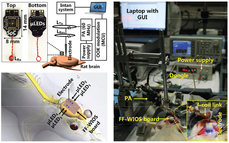
A modified FF-WIOS system was used in these experiments to facilitate the acute animal studies. The FF-WIOS board (14×8 mm2), shown in Fig. 13, consisted of an FF-WIOS SoC bonded on the top side, a 2 ×2 μLED array (0.5 × 1 ×0.4 mm3, LB QH9G, OSRAM) assembled on the bottom side, and LRx soldered at the back-end. A class-E PA delivered power wirelessly to the FF-WIOS board through the optimized 3-coil inductive link at 60 MHz. The FF-WIOS board was placed over the skull of the rats with two μLEDs aligned over each side of V1 lobe. More specifically, μLED1 and μLED2 were above the left V1, while μLED3 and μLED4 were above the right V1.
Fig. 13.
In vivo experimental setup with its block diagram and anatomical location of the FF-WIOS board, electrode, and μLEDs on the rat brain.
Under anesthesia, unilateral optical stimulation was performed on the left V1 by selectively driving μLED1 with user-defined parameters, while LFPs were simultaneously recorded through a tungsten electrode, which penetrated into the left V1 cortical layers. The LFP recordings were amplified and digitalized through a commercial 32-ch Intan system (RHD2132), and then uploaded to a PC for data analysis using a MATLAB Chronux toolbox.
Fig. 14 shows LFPs recorded at the depths of 100 μm, 500 um, and 1 mm, following light stimulation directed with a pulse train of 2 ms pulse width, 2.5 Hz frequency, and 10 mA stimulation current. Clear light-evoked LFPs were observed at the ~100 μm depth, in response to the optical stimulation, whereas the LFP variation decreases as the recording depth increases. This result reveals that the optical stimulation applied by the FF-WIOS can evoke the neurons in superficial layers.
Fig. 14.
LFP recordings at different depths through the tungsten electrode.
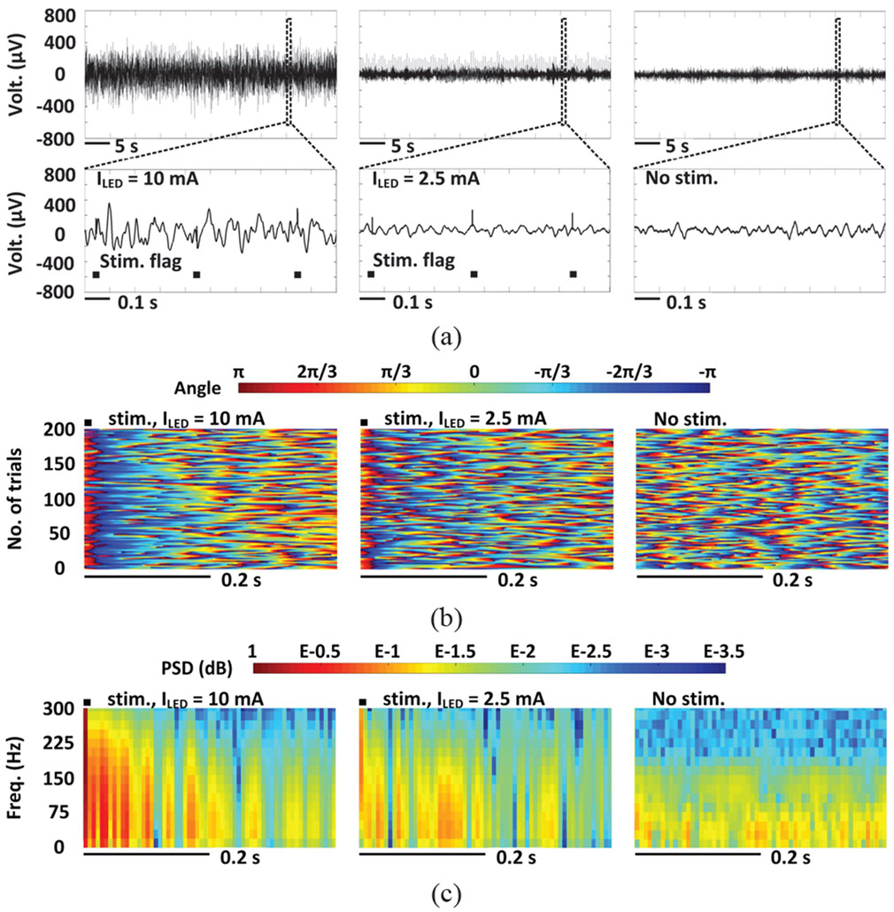
At the effective stimulation depth of 100 μm, LFPs were measured when the μLED light intensity is above and below the threshold of 1 mW/mm2 [27]. The stimulation pulses have 2 ms pulse width at 2.5 Hz with 10 mA and 2.5 mA current limits, corresponding to the light intensity of ~10 mW/mm2 and ~0.95 mW/imn2, respectively. Spontaneous LFPs were also recorded as a baseline when μLEDs were completely off. We expected to observe light-evoked LFPs, i.e. synchronized with above-threshold stimulation, being distinguishable from the LFPs uncorrelated with below-threshold stimulation.
LPF recordings recorded at different light intensity are compared in Fig. 15a over a time span of 50 s. The stimulation flags in the close-up view of 1 s long LFP recordings indicate the occurrence of a stimulation pulse. Photoelectric artifacts induced from light stimulation came along with the LFPs [3], [4]. The recorded LFPs with below-threshold stimulation is not evoked as compared to the spontaneous LFPs, while with 10 mA stimulation current, the recorded LFPs show significantly larger variations, suggesting that the above-threshold stimulation can effectively evoke neural activity.
Fig. 15.
LFP analysis in terms of (a) amplitude variation, (b) instantaneous phases, and (c) normalized PSD with above threshold stimulation (left), below threshold stimulation (middle), and no stimulation (right).
The Hilbert transformation was applied to extract the instantaneous phases of 200 trials of LFP recordings within a frequency range of 1-25 Hz [10], [44]. In Fig. 15b, colors indicate the instantaneous phase of each trial. The 200 trials are aligned to the concurrence of the stimulus and stacked. The Y axis of the Hilbert transformation in Fig. 15b is the number of trials. Since each trial lasts 0.4 s, the X axis of the Hilbert transformation indicates the time duration of the stimulation trials. The instantaneous phase of individual trial is color coded, aligned to the concurrence of the stimulus, and stacked as shown in Fig. 15b. Expectedly, the spontaneous LFPs with random phases did not show phase synchrony. Very short phase synchrony was observed at the 2.5 mA stimulation current, which could be the effect of photoelectric artifacts. In contrast, strong and reliable phase-locked synchronization was observed across 200 trials within a time window of ~100 ms following the optical stimulation at 10 mA current (p < 0.05, Wilcoxon signed rank test).
Furthermore, 200 trial LFPs were averaged and mapped onto a time-frequency graph of color-coded, normalized power spectral density (PSD) distribution [10], [45]. Fig. 15c shows the PSD results in a 1-300 Hz frequency range, where a significant increase in PSD was observed in a short time window of ~100 ms following the optical stimulation of 10 mA. In contrast, stimuli at 2.5 mA only caused a slight increase in PSD as compared to the PSD of the spontaneous LFPs, which can be mainly attributed to the photoelectric artifacts.
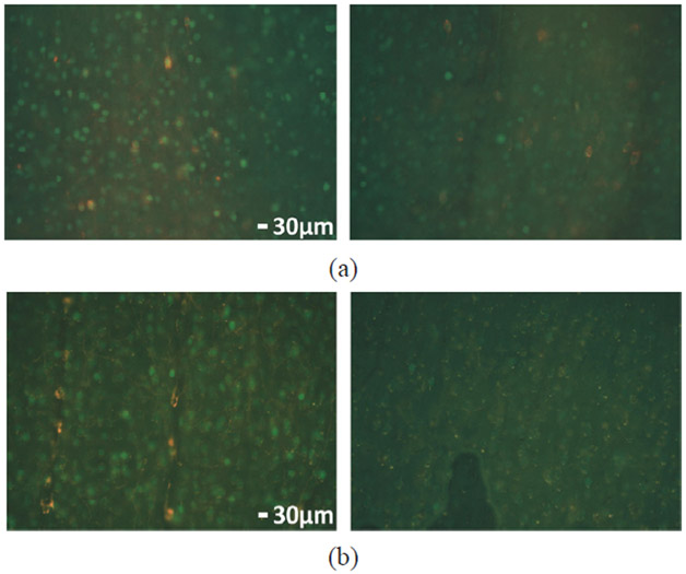
In addition to LFPs, immunochemical analysis was performed to identify the increased expression of c-Fos as an indirect measure of light-evoked neuronal activity induced by optical stimulation [10], [46]. In this experiment, the left V1 lobes of both rat #1 and #2 were stimulated optically for 45 mins, with 2 ms pulse width, 2.5 Hz pulse rate, and 10 mA stimulation current, while the right V1 was untouched as a control. Fig. 16 shows the fluorescent microscope images of the post-processed brain tissue with a thickness of 50 μm. Green fluorescence spots indicate cells expressing c-Fos, while orange spots are m-cherry stained cells that are expressing optogenetic opsins (ChR2). The tissue analysis results show a significant increase in the c-Fos expression under 10 mA stimulation, implying elevated neural activity. In contrast, only a slight increase in the c-Fos expression was observed at the 2.5 mA current, most likely representative of background activity since both of the rats’ eyes were open during testing [10]. Moreover, the overlapping of the cells expressing both m-cherry and c-Fos reveals that the same transfected cells express increased activities induced by the above-threshold optical stimulation.
Fig. 16.
C-Fos expression in left and right V1 lobes of (a) rat #1 and (b) rat #2.
D. Miniature FF-WIOS Prototype and In Vitro Experiment
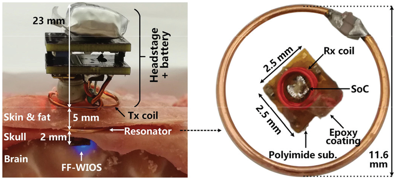
Fig. 17 shows the in vitro setup using tissue layers in a cube cut out of a sheep head, including brain, skull, fat, and skin for preliminary evaluation of the system operation. The headstage, powered by a 100 mAh rechargeable LiPo battery, weights 4.2 g. The assembled FF-WIOS and LRes are encapsulated with 5 μm Parylene-C and ~50 μm PDMS before implantation. The FF-WIOS implant, with dimensions and weight of 2.5×2.5×1.5 mm3 and 15 mg, respectively, is placed on the surface of the brain, while LRes is placed above the skull but under the scalp, well aligned with and 2 mm away from the FF-WIOS implant. Between LTx and LRes is the skin and fat layers of scalp with a total thickness of 5 mm. The headstage is placed above the skin and concentrically aligned with LRES. In this setup, the headstage delivered sufficient power to operate the FF-WIOS by driving a selected μLED (blue color), while the MCU established BLE link with PC and OOK modulated the power carrier, resulting in 97.6 mW drawn from the 3.7 V battery.
Fig. 17.
In vitro measurement setup using the sheep model with a close-up view of the FF-WIOS and the resonator.
VI. Conclusion and Future Steps
We have presented a wirelessly-powered free-floating implantable optical stimulation device. With its compact size and light weight, the FF-WIOS is expected to minimize tissue damage and therefore enable efficient chronic wireless optical stimulation. Thanks to the 3-coil inductive link design, the FF-WIOS is efficiently powered, while staying well below the SAR limit. Wireless data transmission between the headstage and FF-WIOS is established with OOK modulation of the power carrier. The CLPC mechanism is also utilized to ensure stable power delivery to the FF-WIOS. The SCS architecture implemented in the FF-WIOS SoC provides high instantaneous current for effective optical stimulation without putting too much burden on the inductive link. The circuit topology for each block is chosen for power/area efficiency and design simplicity to achieve a compact and reliable SoC design. It is possible to further reduce power consumption using ultra-low power circuit designs, e.g. the relaxation oscillator design in [47]. We have verified the functionality of the entire system in vitro and in vivo on sheep head and rat models, respectively. We targeted the left V1 of two anesthetized rats with wireless optical stimulation, while observing light-evoked LFPs and immunostained tissue responses. Table III benchmarks the FF-WIOS against state-of-art optical implants in the literature. The FF-WIOS is competitive in terms of implant size, weight, and stimulation capability. The near-field 3-coil link combined with SCS charge storage is a safe and efficient strategy that can offer sufficient PDL for optical stimulation. Moreover, CLPC can handle misalignments much better than ultrasound and focused EM field at high frequencies. The FF-WIOS also benefits from high-level integration of 16-ch stimulation and provides the end user with full control over the stimulation parameters.
Table III.
Benchmarking of mm-Sized. Wirelessly Powered Optogenetic Interfaces
| Publication | [17] | [18] | [19] | [20] | [21] | This work | |
|---|---|---|---|---|---|---|---|
| Technology | COTS | COTS | COTS | 0.35-μ CMOS | 0.18-μ HV BCD | 0.35-μ CMOS | |
| Wireless power, operating Freq. | RF, 1.5 GHz | RF, 2.9 GHz | RF, 13.56 MHz | Photovoltaic | Ultrasound, 1.314 MHz | RF, 60 MHz | |
| Number of stim. channels | 1 | 4 | 1 | 1 | 4 | 16 | |
| Max. ILED (mA) | - | - | 20 | 5 | 5 | 10 | |
| Light intensity (mW/mm2) | 1-60 | 30 | 1-50 | 15 | 1.4-23 | Up to 10 | |
| Stimulation Power eff.** % | 19* | - | - | 10.7* | 50.3** | 37.5** | |
| efficiency * Optical eff.*** % | - | - | 30.7*** | 62.5*** | |||
| Device size (mm3) | 10-25 | 125 | 9.8 mm diameter, 1.3 mm thickness | 1.3×1.3 ×(0.6-1.0) | 2×3×6.5 | 2.5×2.5×1.5 (in vivo) | 8×14×2 (in vivo) |
| Device weight | 20-50 | 220 | 30 | 2.3 | 78 | 15 mg (in vitro) | 0.5 g (in vivo) |
| Stim. proper Ctrl | No | No | No | No | Yes | Yes | |
| In vivo experiments | Yes | Yes | Yes | No | Yes | Yes | |
Stim. eff. = power eff. × optical eff.
Power eff. = rectifier eff. × LDO eff.
Optical eff: output light power divided by input power.
The FF-WIOS prototype used for in vitro experiments is the miniaturized version of the FF-WIOS prototype used in vivo. By the miniaturized version of FF-WIOS, we are referring to the prototype built on polyimide substrate. We are now working towards testing this miniaturized version in vivo, first on an anesthetized rats and then on freely behaving subjects within the EnerCage-HC environment [33], [34]. Since the miniaturized version has smaller Cree μLEDs assembled, the resolution of optical stimulation applied using this prototype can be improved. It is also possible to couple a fiber onto the μLED to further focalize LED light onto a specific brain area at the cost of being more invasive [48]. This miniaturized version of the FF-WIOS is built on polyimide substrate, which is flexible and biocompatible. It is an important step towards the free-floating distributed neural interface concept.
From the neuroscience perspective of alignment with a particular target in the brain, a combination of multiple FF-WIOS distributed within the region of interest, and each FF-WIOS being capable of driving a 4×4 μLED array with 700 μm pitch, give the neuroscientist sufficient flexibility, redundancy, and leeway to try multiple adjacent channels or nearby devices to find the optimal target. In rodents, surgery procedure involves creating small holes in the skull that match the size of FF-WIOS at the target locations. After placing the device, the hole will be sealed by dental cement. This approach would preserve key feature of the FF-WIOS to be free-floating with no anchor onto the skull or brain tissues, and minimize damage to the surrounding tissue. Due to small intracranial space and thinness of the skull bone, LRes will be placed above the skull but under the scalp to power the FF-WIOS devices underneath through the bone. LRes is stationary and covers the target brain area. Therefore, no accurate alignment is needed when one or more FF-WIOS are to be located within LRes, and as we have demonstrated before [38], every one of them can receive sufficient power regardless of their position.
Acknowledgments
This work is supported in part by NSF awards ECCS-1407880 and ECCS-1408318, and NIH award 1R21EB018561.
Contributor Information
Yaoyao Jia, School of Electrical and Computer Engineering, Georgia Institute of Technology, Atlanta, GA 30308, USA..
S. Abdollah Mirbozorgi, Department of Electrical and Computer Engineering, University of Alabama at Birmingham, AL 35294, USA..
Byunghun Lee, Department of Electrical and Computer Engineering, Incheon National University, Incheon, South Korea.
Wasif Khan, Department of Electrical and Computer Engineering, Michigan State University, East Lansing, MI 48824, USA.
Fatma Madi, Department of Physiology, Michigan State University, East Lansing, MI 48824, USA.
Omer T. Inan, School of Electrical and Computer Engineering, Georgia Institute of Technology, Atlanta, GA 30308, USA.
Arthur Weber, Department of Physiology, Michigan State University, East Lansing, MI 48824, USA.
Wen Li, Department of Electrical and Computer Engineering, Michigan State University, East Lansing, MI 48824, USA.
Maysam Ghovanloo, School of Electrical and Computer Engineering, Georgia Institute of Technology, Atlanta, GA 30308, USA.
References
- [1].Deisseroth K, “Optogenetics,” Nat. Methods, vol. 8, no. 1, pp. 11–23, January 2011. [DOI] [PMC free article] [PubMed] [Google Scholar]
- [2].Rivnay J et al. , “Next-generation probes, particles, and proteins for neural interfacing,” Science Advances, vol. 3, no. 6, p. 1601649, June 2017. [DOI] [PMC free article] [PubMed] [Google Scholar]
- [3].Goncalves SB et al. , “Design and manufacturing challenges of optogenetic neural interfaces: a review,” J. Neural Eng, vol. 14, no. 4, p. 041001, May 2017. [DOI] [PubMed] [Google Scholar]
- [4].Fan B and Li W, “Miniaturized optogenetic neural implants: a review,” Lab Chip, vol. 15, no. 19, pp. 3838–3855, August 2015. [DOI] [PubMed] [Google Scholar]
- [5].LeChasseur Y et al. , “A microprobe for parallel optical and electrical recordings from single neurons in vivo,” Nat. Methods, vol. 8, no. 4, pp. 319–325, April 2011. [DOI] [PubMed] [Google Scholar]
- [6].Dufour S et al. , “A multimodal micro-optrode combining field and single unit recording, multispectral detection and photolabeling capabilities,” PloS One, vol. 8, no. 2, p. e57703, February 2013. [DOI] [PMC free article] [PubMed] [Google Scholar]
- [7].Wang J et al. , “Integrated device for combined optical neuromodulation and electrical recording for chronic in vivo applications,” J. Neural Eng., vol. 9, no. 1, p. 016001, December 2011. [DOI] [PubMed] [Google Scholar]
- [8].Tamura K et al. , “A glass-coated tungsten microelectrode enclosing optical fibers for optogenetic exploration in primate deep brain structures,” J. Neurosci. Methods, vol. 211, no. 1, pp. 49–57, October 2012. [DOI] [PubMed] [Google Scholar]
- [9].Kwon KY et al. , “Opto-μECoG array: a hybrid neural interface with transparent μECoG electrode array and integrated LEDs for optogenetics,” IEEE Trans. Biomed. Circuits Syst, vol. 7, no. 5, pp. 593–600, October 2013. [DOI] [PubMed] [Google Scholar]
- [10].Jia Y et al. , “Wireless opto-electro neural interface for experiments with small freely behaving animals,” J. Neural Eng, vol. 15, no. 4, p. 046032, June 2018. [DOI] [PMC free article] [PubMed] [Google Scholar]
- [11].Jia Y, et al. , “A closed-loop wireless homecage for optogenetic stimulation experiments,” IEEE Biomed. Circuits Syst. Conf Atlanta, FL, USA, 2015, pp. 1–4. [Google Scholar]
- [12].Hashimoto M et al. , “Programmable wireless light-emitting diode stimulator for chronic stimulation of optogenetic molecules in freely moving mice,” Neurophotonics, vol. 1, no. 1, p. 011002, May 2014. [DOI] [PMC free article] [PubMed] [Google Scholar]
- [13].Jeong JW et al. , “Wireless optofluidic systems for programmable in vivo pharmacology and optogenetics,” Cell, vol. 162, no. 3, pp. 662–674, July 2015. [DOI] [PMC free article] [PubMed] [Google Scholar]
- [14].Gagnon-Turcotte G et al. , “A wireless headstage for combined optogenetics and multichannel electrophysiological recording,” IEEE Trans. Biomed. Circuits Syst, vol. 11, no. 1, pp. 1–14, February 2017. [DOI] [PubMed] [Google Scholar]
- [15].Lee ST et al. , “A miniature, fiber-coupled, wireless, deep-brain optogenetic stimulator,” IEEE Trans. Neural Syst. Rehabilitation. Eng, vol. 23, no. 4, pp. 655–664, July 2015. [DOI] [PubMed] [Google Scholar]
- [16].McConnell GC et al. , “Implanted neural electrodes cause chronic, local inflammation that is correlated with local neurodegeneration,” J. Neural Eng, vol. 6, no. 5, p. 056003, August 2009. [DOI] [PubMed] [Google Scholar]
- [17].Montgomery KL et al. , “Wirelessly powered, fully internal optogenetics for brain, spinal and peripheral circuits in mice,” Nat. Methods, vol. 12, no. 10, pp. 969–974, August 2015. [DOI] [PMC free article] [PubMed] [Google Scholar]
- [18].Noh KN et al. , “Miniaturized, battery-free optofluidic systems with potential for wireless pharmacology and optogeneticstics,” Small, vol. 14, no. 4, p. 1702479, January 2018. [DOI] [PMC free article] [PubMed] [Google Scholar]
- [19].Shin G et al. , “Flexible near-field wireless optoelectronics as subdermal implants for broad applications in optogenetics,” Neuron, vol. 93, no. 3, pp. 509–521, February 2017. [DOI] [PMC free article] [PubMed] [Google Scholar]
- [20].Tokuda T et al. , “1 mm3-sized optical neural stimulator based on CMOS integrated photovoltaic power receiver,” AIP Advances, vol. 8, no. 4, p. 045018, April 2018. [Google Scholar]
- [21].Charthad J et al. , “A mm-sized wireless implantable device for electrical stimulation of peripheral nerves,” IEEE Trans. Biomed. Circuits Syst, vol. 12, no. 2, pp. 257–270, April 2018. [DOI] [PubMed] [Google Scholar]
- [22].IEEE Standard for Safety Levels with Respect to Human Exposure to Radio Frequency Electromagnetic Fields, 3 kHz to 300 GHz, IEEE Standard C95.1–2005. 2005.
- [23].Amar AB, Kouki AB, and Cao H, “Power approaches for implantable medical devices,” Sensors, vol. 15, no. 11, pp. 28889–28914, November 2015. [DOI] [PMC free article] [PubMed] [Google Scholar]
- [24].Jia Y et al. , “A mm-sized free-floating wirelessly powered implantable optical stimulating system-on-a-chip,” IEEE International Solid-State Circuits Conf, San Francisco, CA, USA, 2018, pp. 468–470. [Google Scholar]
- [25].Jia Y et al. , “Towards a free-floating wireless implantable optogenetic stimulating system,” IEEE International Midwest Symp. Circuits Syst. Conf, Boston, MA, USA, 2017, pp. 381–384. [Google Scholar]
- [26].Khan W et al. , “A miniaturized, wirelessly-powered, reflector-coupled single channel opto neurostimulator,” IEEE Micro Mech. Syst, Belfast, Northern Ireland, 2018, pp. 174–177. [Google Scholar]
- [27].Stark E, Koos T, and Buzsaki G, “Diode probes for spatiotemporal optical control of multiple neurons in freely moving animals,” J. Neurophysiol, vol. 108, no. 2, pp. 349–363, July 2012. [DOI] [PMC free article] [PubMed] [Google Scholar]
- [28].Lee H et al. , “A power-efficient switched-capacitor stimulating system for electrical/optical deep brain stimulation,” IEEE J. Solid-State Circuits, vol. 50, no. 1, pp. 360–374, January 2015. [Google Scholar]
- [29].Baker RJ, “Special purpose CMOS circuits,” in CMOS circuit design, layout, and simulation, 3nd ed. Hoboken, NJ, U.S.: John Wiley & Sons, Inc., 2010, pp. 523–529. [Google Scholar]
- [30].Lee B et al. , “An implantable peripheral nerve recording and stimulation system for experiments on freely moving animal subjects,” Scientific Reports, vol. 8, no. 1, p. 6115, April 2018. [DOI] [PMC free article] [PubMed] [Google Scholar]
- [31].Kiani M and Ghovanloo M, “An RFID-based closed-loop wireless power transmission system for biomedical applications,” IEEE Trans. Circuits Syst. II, vol. 57, no. 4, pp. 260–264, April 2010. [DOI] [PMC free article] [PubMed] [Google Scholar]
- [32].Lee B, Kiani M, and Ghovanloo M, “A triple-loop inductive power transmission system for biomedical applications,” IEEE Trans. Biomed. Circuits Syst, vol. 10, no. 1, pp. 138–148, February 2016. [DOI] [PubMed] [Google Scholar]
- [33].Mirbozorgi SA et al. , “A wirelessly-powered homecage with segmented copper foils and closed-loop power control,” IEEE Trans. Biomed. Circuits Syst, vol. 10, no. 5, pp. 979–989, October 2016. [DOI] [PMC free article] [PubMed] [Google Scholar]
- [34].Jia Y et al. , “Position and orientation insensitive wireless power transmission for EnerCage-Homecage system,” IEEE Trans. Biomed. Eng, vol. 64, no. 10, pp. 2439–2449, October 2017. [DOI] [PMC free article] [PubMed] [Google Scholar]
- [35].Ghovanloo M and Najafi K, “Fully integrated wideband high-current rectifiers for inductively powered devices,” IEEE J. Solid-State Circuits, vol. 39, no. 11, pp. 1976–1984, November 2004. [Google Scholar]
- [36].Lee H and Ghovanloo M, “A high frequency active voltage doubler in standard CMOS using offset-controlled comparators for inductive power transmission,” IEEE Trans. Biomed. Circuits Syst, vol. 7, no. 3, pp. 213–224, June 2013. [DOI] [PMC free article] [PubMed] [Google Scholar]
- [37].Ahn D and Ghovanloo M, “Optimal design of wireless power transmission links for millimeter-sized biomedical implants,” IEEE Trans. Biomed Circuits Syst, vol. 10, no. 1, pp. 125–137, February 2016. [DOI] [PubMed] [Google Scholar]
- [38].Mirbozorgi SA, Yeon P, and Ghovanloo M, “Robust wireless power transmission to mm-sized free-floating distributed implants,” IEEE Trans. Biomed. Circuits Syst, vol. 11, no. 3, pp. 692–702, June 2017. [DOI] [PubMed] [Google Scholar]
- [39].Yeon P et al. , “Feasibility study on active back telemetry and power transmission through an inductive link for millimeter-sized biomedical implants,” IEEE Trans. Biomed. Circuits Syst, vol. 11, no. 6, pp. 1366–1376, December 2017. [DOI] [PubMed] [Google Scholar]
- [40].Kiani M, Jow UM, and Ghovanloo M, “Design and optimization of a 3-coil inductive link for efficient wireless power transmission,” IEEE Trans. Biomed. Circuits Syst, vol. 5, no. 6, pp. 579–591, December 2011. [DOI] [PMC free article] [PubMed] [Google Scholar]
- [41].Gias C et al. , “Retinotopy within rat primary visual cortex using optical imaging,” NeuroImage, vol. 24, no. 1, pp. 200–206, January 2005. [DOI] [PubMed] [Google Scholar]
- [42].Jia Y, Mirbozorgi SA, Zhang P, Inan OT, Li W, and Ghovanloo M, “A dual-band wireless power transmission system for evaluating mm-sized implants,” IEEE Trans. Biomed. Circuits Syst, under review, 2019. [DOI] [PMC free article] [PubMed] [Google Scholar]
- [43].“CHIPLED 0402 Datasheet,” Osram. Munich, Germany. Version 1.2 LT QH9G, September 2005. [Online] Available: https://www.osram.com/media/resource/hires/osram/LT%20QH9G.pdf
- [44].Quyen MLV et al. , “Comparison of Hilbert transform and wavelet methods for the analysis of neuronal synchrony,” J. Neurosci. Methods, vol. 111, no. 2, pp. 83–98, October 2004. [DOI] [PubMed] [Google Scholar]
- [45].Leuthardt EC et al. , “A brain-computer interface using electrocorticographic signals in humans,” J. Neural Eng, vol. 1, no. 2, pp. 63–71, June 2004. [DOI] [PubMed] [Google Scholar]
- [46].Kawashima T, Okuno H, and Bito H, “A new era for functional labeling of neurons: activity-dependent promoters have come of age,” Front. Neural Circuits, vol. 8, no. 37, April 2014. [DOI] [PMC free article] [PubMed] [Google Scholar]
- [47].Dai S and Rosenstein JK, “A 14.4nW 122KHz dual-phase current-mode relaxation oscillator for near-zero-power sensors,” IEEE Custom Integrated Circuits Conference (CICC), San Jose, CA, 2015, pp. 1–4. [Google Scholar]
- [48].Kwon KY, Lee H, Ghovanloo M, Weber A, and Li W, “Design, fabrication, and packaging of an integrated, wirelessly-powered optrode array for optogenetics application,” Front. Syst. Neurosci, vol. 9, no. 69, May 2015. [DOI] [PMC free article] [PubMed] [Google Scholar]


