Abstract
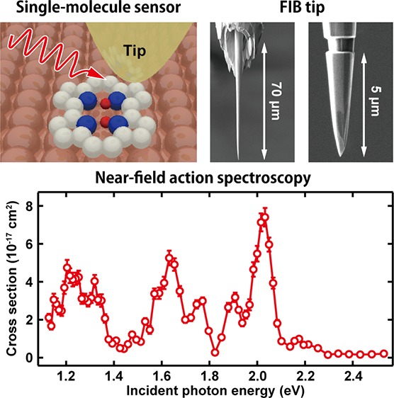
The near-field spectral response of metallic nanocavities is a key characteristic in plasmon-assisted photophysical and photochemical processes. Here, we show that the near-field spectral response of an optically excited plasmonic scanning tunneling microscope (STM) junction can be probed by single-molecule reactions that serve as a nanoscale sensor detecting the local field intensity. Near-field action spectroscopy for the cis ↔ cis tautomerization of porphycene on a Cu(110) surface reveals that the field enhancement in the STM junction largely depends on microscopic structures not only on the tip apex, but also on its shaft. Using nanofabrication of Au tips with focused ion beam, we show that the spectral response is strongly modulated through the interference between the localized surface plasmon in the junction and propagating surface plasmon polariton generated on the shaft. Furthermore, it is demonstrated that the near-field spectral response can be manipulated by precisely shaping the tip shaft.
Nanostructures made of coinage metals strongly interact with visible light through excitation of localized surface plasmon resonance (LSPR) and nanocavities are of particular interest due to extreme confinement and enhancement of an electromagnetic field.1 The LSPR excitation also leads to the (re)emission of a photon, the generation of hot carriers, and local heating.2 These consequences contribute to plasmon-mediated photochemical processes such as surface enhanced spectroscopy,3 near-field-induced charge transfer and separation,4,5 and photochemical reactions.6 The hot-carrier generation plays a crucial role in plasmon-induced processes such as enhanced photocurrent generation and photocatalysis.7 The energy distribution and dynamics of the plasmon-induced hot carriers govern the subsequent processes, which are determined by material, size, and shape of nanostructures8 and theoretical studies have provided valuable insights into the microscopic mechanisms.9 However, the underlying mechanisms of plasmon-induced carrier formation remain poorly understood because it is difficult to directly observe such a nonradiative decay due to the lack of appropriate experimental methods.
For plasmon-induced photochemical reactions, the hot-carrier mediated mechanism is considered to be dominant in many cases.10−12 A more-recent study also addresses quantifying the relative contribution between plasmon-induced hot carriers and thermal activation.13 In plasmonic catalysis, the microscopic reaction mechanism also depends on the local adsorption structure and electronic state of molecules as well as the local field enhancement over plasmonic nanostructures. However, the direct observation of plasmon-induced reactions is still a challenging task. Low-temperature scanning tunneling microscopy (STM) combined with optical excitation has recently demonstrated its unique capability to investigate plasmon-induced reactions at the single-molecule level.14,15 Our previous study shows that the single-molecule tautomerization of porphycene can be largely enhanced by the plasmon-induced hot-carrier generation, and the wavelength-dependent reaction cross-section, what we call near-field action spectroscopy, can reveal the near-field spectral response in a plasmonic STM junction.14 We also found that the near-field action spectrum, corresponding to the spectral response of the gap plasmon, is sensitive to the tip.14 Although it has been well-known from both experiment and theory that the spectral response of gap plasmons in STM junctions is susceptive to the tip shape,16−19 the correlation between the microscopic tip shape and the local field enhancement remains imperfectly understood. Here we examine the role of the microscopic tip structure in great detail using near-field action spectroscopy in combination with nanoscale tip fabrication by using a focused ion beam (FIB). It is revealed that microscopic structures not only on the tip apex but also on its shaft largely affect the local field enhancement in the optically excited junction. Our results demonstrate that single-molecule reactions in a plasmonic STM junction serve as a nanoscale sensor to detect the localized field and that the interference between the LSP in the junction and propagating surface plasmon polaritons (SPPs) generated on the tip shaft strongly modulates the near-field spectral response in the junction.
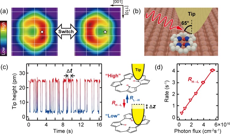
Figure 1a shows STM images of a single porphycene molecule on the Cu(110) surface at 5 K, where the molecule adsorbs in the cis configuration and flips between two mirror-reflected states via the cis ↔ cis tautomerization.20Figure 1b displays the schematic of the experiment. The lateral tip position was fixed over the molecule at the location indicated in Figure 1a. The bias voltage was set below the threshold of tunneling electron-induced tautomerization (<|150| mV), and thermal excitation is negligible at 5 K.21 The junction was then illuminated by a wavelength-tunable laser to induce the tautomerization. Although thermal expansion of the tip (and sample) occurred upon illumination, the feedback control of the STM ensured avoiding destruction of the junction. This thermal expansion equilibrated in about 10–20 min after starting the illumination. All subsequent measurements were conducted under stationary conditions. We used a ∼2 mm beam spot with a homogeneous top-hat profile to minimize possible systematic errors arising from the beam alignment with respect to the STM junction.22 The tautomerization under the tip can be monitored by a change in the tip height, manifested as a random telegraph signal between two states (Figure 1c). The tautomerization rate was obtained by statistical analysis of the dwell time of the “high” and “low” states. Note that the transition of “high”→ “low” and “low”→ “high” is not equivalent due to the presence of the tip that breaks the symmetry of the system and each tautomerization rate is denoted by RH→L and RL→H, respectively. The near-field induced process shows a linear dependence on the incident laser power (Figure 1d), indicating that the reaction occurs via a single-photon process.
Figure 1.
(a) STM images of porphycene on Cu(110) at 5 K. (b) Schematic of the experiment. (c) Tip height trace under 690 nm illumination (6 K, Vt = 50 mV, and It = 10 pA). The lateral tip position during the measurement is indicated by stars in panel a. On the right, “high” and “low” states are illustrated. (d) Photon flux dependence of the tautomerization rate (RH→L) obtained with 690 nm excitation (6 K, Vt = 50 mV, and It = 10 pA).
Figure 2 shows the lateral tip position dependence of the tautomerization rate by near-field excitation and by injection of tunneling electrons from the STM. In both cases, the rate rapidly decreases as the tip moves laterally away from the molecule. The distribution of the tautomerization rate appears to correlate with the STM appearance of the molecule, i.e., the local density of states. This result indicates that the hot-carrier transfer between the molecule and the tip apex via tunneling plays a dominant role in the near-field induced process, which is consistent with our previous study on Cu(111).14
Figure 2.
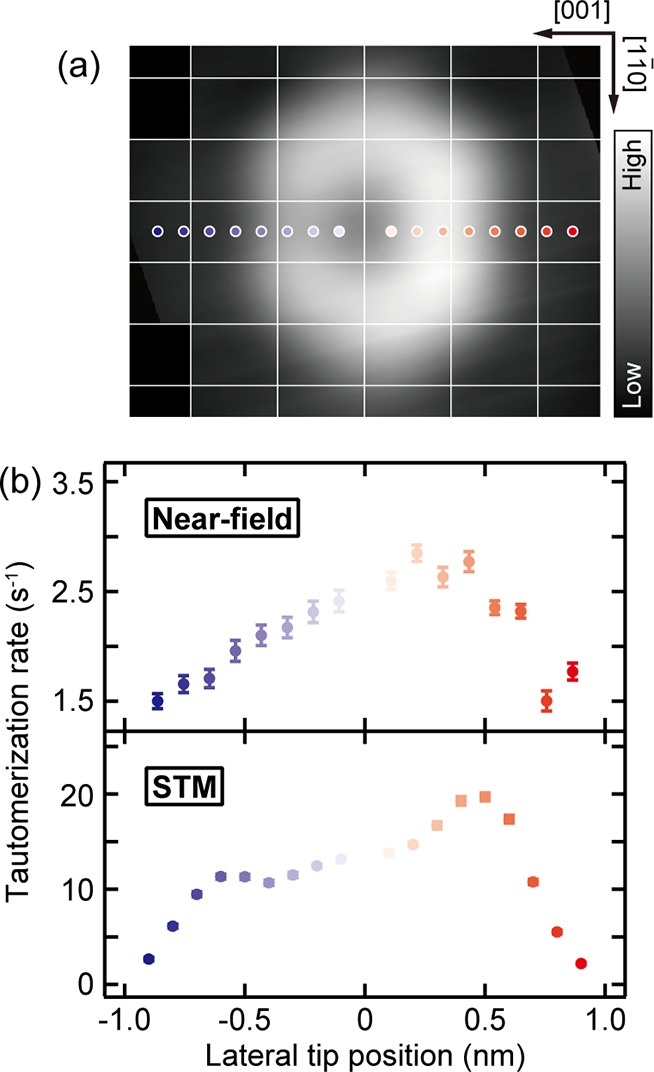
(a) STM image of porphycene. (b) Lateral position dependence of the near-field (top) and STM-induced (bottom) tautomerization rate. The former is measured under 690 nm illumination (6 K, Vt = 50 mV, and It = 10 pA), while the latter is measured at Vt = 350 mV and It = 10 pA. The measurement points are indicated in panel a.
We recorded the near-field action spectra, and the reaction cross-section was obtained by:
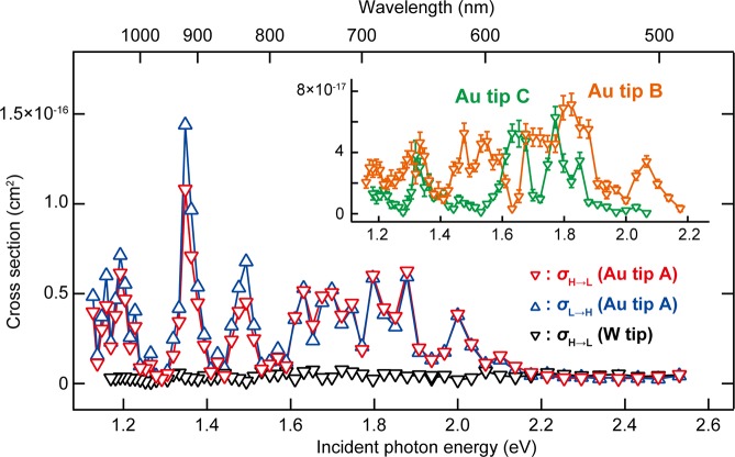
where till is the illumination duration and nph the incident photon fluence. Figure 3 shows the action spectra measured with electrochemically etched Au and W tips. The cross-section for the Au tip is much larger than for W because of the strong field enhancement arising from surface plasmon excitation of an Au tip.23 The decrease of the cross-section above ∼2 eV results from quenching of surface plasmon excitation at the onset of the interband transition of the Cu substrate (2.03 eV).14 Remarkably, the near-field action spectra exhibit many narrow peaks and a qualitatively similar spectral feature is observed for all tips prepared by standard electrochemical etching.24 The inset of Figure 3 shows the action spectra obtained with other Au tips that also exhibit multiple peaks, but their position and intensity differ for each tip. The spectral feature is reproducible unless the tip conditions (shape) are changed by a strong tip forming procedure. A multiple-peak feature has been observed in previous STM-induced luminescence (STML) experiments, and the energy intervals between the adjacent peaks were in the range between 0.1–0.5 eV (e.g., ref (18)), which are assigned to the resonant LSP modes in the junction with a different order. However, this mechanism cannot explain the multiple peaks in our near-field action spectra because the peak intervals are much smaller.
Figure 3.
Near-field action spectra of the cis ↔ cis tautomerization measured with an Au and a W tip. The inset shows the results obtained with other Au tips (6 K, Vt = 50 mV, and It = 10 pA). The incident beam is polarized parallel to the tip (p-polarization).
We also carried out near-field action spectroscopy for a totally different molecular species, namely a hydroxyl dimer (OH)2 on Cu(110) (Figure 4a). The hydroxyl dimer flips between two orientations and the threshold voltage of ∼170 mV25 is comparable to that of the cis ↔ cis tautomerization of porphycene on Cu(110).21Figure 4b shows the action spectra recorded for porphycene and (OH)2 coadsorbed nearby. The cross-section in the near-field action spectroscopy (except for Figure 3) represents the total cross-section that is obtained by analyzing the dwell time without distinguishing the “high” → “low” and “low” → “high” processes. This procedure provides smaller statistical errors but does not change significantly change the spectral features. Both species were measured one after the other under identical tip conditions. The spectra exhibit very similar peak positions for porphycene and (OH)2, thus indicating that the multiple peaks cannot be attributed to molecular properties but to near-field properties of the junction. A difference in the relative intensity between the respective peaks presumably arises from the different electronic structure of porphycene and (OH)2. This result also corroborates that the direct excitation mechanism plays a negligible role because the transition dipole moment of porphycene and (OH)2 should be considerably different.
Figure 4.
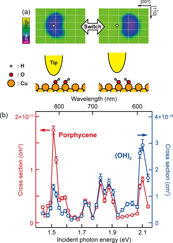
(a) STM images and schematic structure of (OH)2 on Cu(110). (b) Near-field action spectroscopy for porphycene tautomerization (red circles) and (OH)2 flipping (blue circles) with an electrochemically etched Au tip (6 K, Vt = 50 mV, and It = 8 pA). The incident beam is polarized parallel to the tip (p-polarization).
As seen in Figure 3, the near-field action spectra are different from tip to tip, which implies that the tip structure governs the spectral response of the local field enhancement in the junction. Figure 5a,b displays high-resolution scanning electron microscope (SEM) images of an Au tip electrochemically etched from a polycrystalline wire, revealing microscopic structures (surface roughness) on the tip shaft. We speculate that this surface roughness is the cause of the observed spectral fingerprint (multiple-peak feature) in the near-field action spectra. Light can couple to surface plasmons through surface roughness.27,28 Given the experimental setup (the tip is homogeneously illuminated by a laser beam with a spot size of ∼2 mm), surface plasmons can be excited not only in the junction but also on the tip shaft. The SPPs launched on the shaft will undergo random multiple scattering due to the surface roughness and yield a near-field speckle pattern (strong intensity fluctuation), which sensitively depends on the excitation wavelength. Such near-field fluctuations have been observed on disordered (rough) surfaces by SNOM29−31 and have been analyzed theoretically.32 We assume that the SPPs generated on the shaft travel toward the apex and interfere with the LSP in the junction, resulting in the strong spectral fluctuation (Figure 3).
Figure 5.
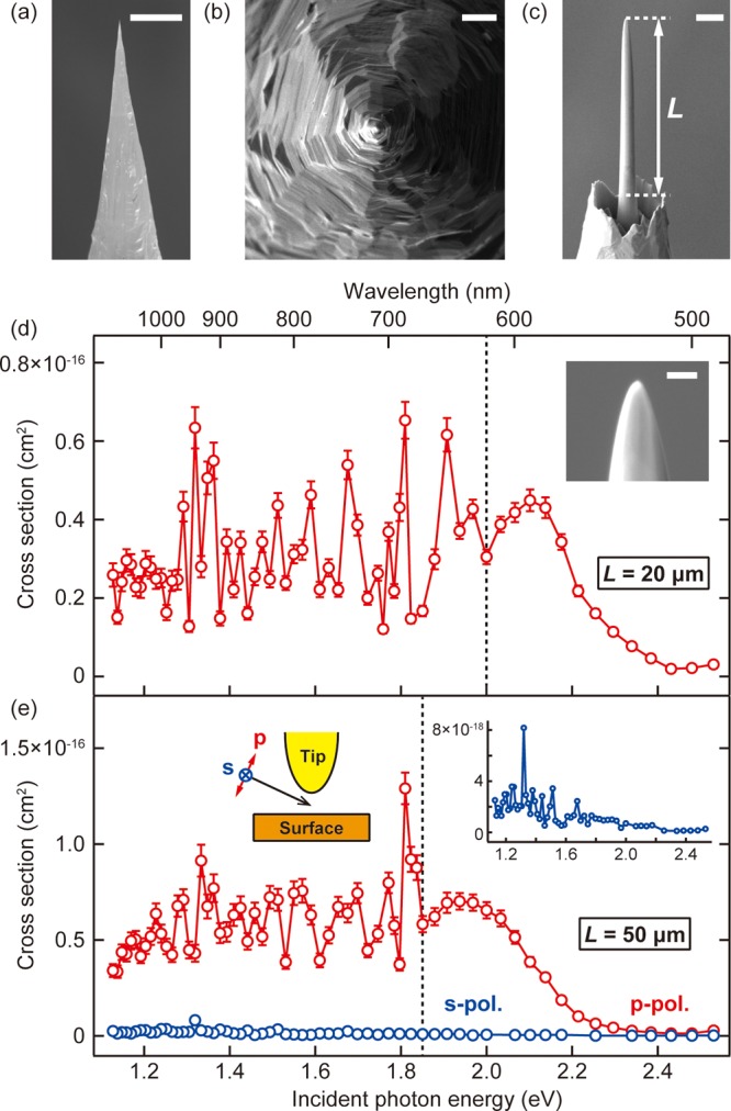
(a, b) SEM images of an electrochemically etched Au tip. The scale bars are 10 and 1 μm in panels a and b, respectively. (c) SEM image of a fabricated Au tip with L = 20 μm. The scale bar is 2 μm. (d) Near-field action spectrum obtained with the fabricated tip in (c) (6 K, Vt = 50 mV, and It = 10 pA). The inset shows the magnified SEM micrograph of the tip apex of panel c, and the scale bar is 200 nm. (e) Near-field action spectrum obtained with a fabricated tip with L = 50 μm. The spectra are measured with a p- (red) and s-polarized (blue) beam (6 K, Vt = 50 mV, and It = 10 pA). The inset shows the vertically magnified spectrum for s-polarization.
To systematically examine the impact of the surface roughness of the tip, we exploited FIB milling to fabricate Au tips with a sharp apex and an extremely smooth shaft (surface roughness of <5 nm), as shown in Figure 5c (denoted hereafter as FIB-tip). Surface plasmon excitation by optical irradiation should be suppressed on this smooth shaft. Figure 5d,e shows the near-field action spectra obtained by the FIB-tips with a smoothed shaft length (L) of about 20 and 50 μm, respectively. The action spectra reveal two distinct regimes: a broad single peak around 2 eV and multiple peaks in the near-infrared (NIR) range (the boundary is indicated by the dashed line in the figures). We explain the emergence of these two regimes as a consequence of the relative contributions from the LSP in the junction and propagating SPPs from the shaft. The broad peak can be assigned to the unperturbed LSP, and its spectral profile is consistent with the STML spectrum.33 However, the near-field speckle has not been observed in STML. This can be explained by the fact that in STML, the LSP is exclusively excited in the junction via inelastic electron tunneling,34 and therefore, it is free from the interference with the propagating SPPs from the shaft, as opposed to spatially extended illumination of the tip in near-field action spectroscopy. At lower photon energies, the multiple peaks occur due to interference of the LSP with propagating SPPs excited at the unprocessed part of the FIB-tip. The resulting SPPs can travel along the smoothed shaft and eventually interfere with the LSP. The propagation length of SPPs is inversely proportional to the excitation photon energy.35 Therefore, at a relatively large photon energy (∼2 eV), the SPPs excited at the unprocessed part substantially decay before reaching the tip apex and the LSP mode dominates the spectral response of the action spectrum. When the smoothed shaft length becomes longer, the SPPs need to travel a larger distance to interfere with the LSP in the junction and, thus, the contribution from the SPPs shifts to a lower photon energy, as seen in Figure 5d,e. We anticipate that the near-field speckle will disappear when the incident beam spot is reduced so that it becomes smaller than the polished shaft length of the FIB-tips.
We also measured the dependence of the action spectrum on the incident light polarization for the 50-μm polished FIB-tip (Figure 5e). The cross-section is much smaller when the incident beam was polarized perpendicular to the tip axis (s-polarization) than that for parallel polarization (p-polarization), indicating weak coupling of the s-polarized light with the surface plasmons. In addition, for s-polarized light, the LSP feature around 2 eV is absent, whereas the speckle feature appears at the lower photon energy range (see the inset of Figure 5e). This indicates that the LSP mode does not contribute to the field enhancement in the junction and the spectral response is governed by the SPPs.
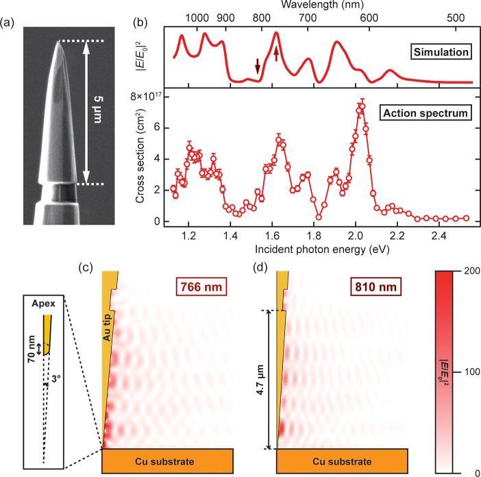
Finally, we examine controlling modulation of the near-field response in the junction by fabricating a single groove on the smoothed shaft, which acts as both coupler and scatterer for SPPs. Figure 6a displays an SEM image of an Au tip with a groove (width of ∼735 nm and depth of ∼200 nm) located at a ∼5 μm distance from the apex (the total polished length is ∼70 μm). Figure 6b shows the near-field action spectrum obtained with this tip, and the spectral response differs either from the unprocessed tips (Figure 3) or from the polished FIB-tips (Figure 5d,e). In particular, the sharpness of multiple peaks is more moderate for the grooved tip than for the others (see the Supporting Information).
Figure 6.
(a) SEM micrograph of a grooved Au tip. The polished length is 75 μm. A 200 nm deep and 735 nm wide groove is milled on the tip shaft at a distance of 5 μm away from the apex. (b) Near-field action spectrum (bottom) and simulated field enhancement in the junction (top) as a function of incident photon energy (6 K, Vt = 50 mV, and It = 10 pA). The incident beam is polarized parallel to the tip (p-polarization). (c, d) Two-dimensional maps of the field enhancement at 765 and 810 nm for the grooved tip. Geometry of the simulation is shown in the inset of panel c.
The well-defined geometry of the grooved tip allows us to simulate the field enhancement in the junction. To gain insights into the interference mechanism, we numerically calculated the spectral response for a simple two-dimensional model using a finite element method, implemented with COMSOL 5.3, RF module. The experimental geometry was approximated by a radially symmetric, spatially extended plane wave excitation (p-polarized) of an Au tip located at 0.6 nm distance from a Cu surface. The structural parameters of the tip were approximated from the SEM micrograph (Figure 5c). We found that a taper angle of 3°, apex diameter of 70 nm, groove position of 4.7 μm from the apex, and incident illumination angle of 61.5° show good agreement with the experimental result (the top panel in Figure 6b). The difference between the experimental and simulated spectra as well as the deviation of the tip structure and incident beam angle (nominally 65° in the experiment) will be acceptable for the simple model here. Figure 6c,d displays a two-dimensional map of the electric field intensity calculated for 766 and 810 nm incident wavelength, corresponding to a local maximum and minimum of the field enhancement, respectively. The simulations show that surface plasmon standing waves are formed on the tip shaft through the excitation and reflection of the SPPs by the groove. As a consequence, depending on the incident photon energy, either constructive or destructive interference occurs in the junction and yields a specific modulation of the local field enhancement. A similar surface plasmon standing wave has been observed for nanowires36−40 and a nanotip.41
In summary, we demonstrated that single-molecule tautomerization of porphycene acts as a nanoscale sensor to detect the near field in the optically excited STM junction. Near-field action spectroscopy revealed the strongly modulated spectral response for electrochemically etched Au tips. Controlled experiments using nanofabrication of Au tips with FIB elucidated that the localized field in the junction sensitively depends on nanoscale structures not only on the tip apex, but also on its shaft. It was also shown that the spectral modulation can be controlled by precisely shaping the tip shaft. As an example, we produced a single groove on a smooth tip shaft to yield a standing wave formation of the SPPs on the shaft and a specific interference with the LSP in the junction. The local field enhancement in (sub)nanometric cavities is of particular interest in ultrasensitive near-field spectroscopy,42 which exhibits an extremely high spatial resolution, even at the submolecular level.43,44 Single-molecule near-field sensor will be useful to examine the nature of extremely confined light.
Methods
All experiments were performed in an ultrahigh-vacuum chamber (base pressure of <10–10 mbar), equipped with a low-temperature STM. The near-field action spectroscopy was conducted with a modified Omicron LT-STM combined with a wavelength tunable laser (Supercontinuum source from NKT Photonics) that provides a spectral bandwidth of 6–8 nm in the visible and <5 nm in the red to NIR range. The bias voltage was applied to the tip (denoted as Vt). The Cu(110) surface was cleaned by repeated cycles of argon ion sputtering and annealing to 700–800 K. Porphycene molecules were deposited from a Knudsen cell (at an evaporation temperature of 450–500 K). The STM tips were made from polycrystalline Au and W wires by electrochemical etching. We used an FEI Helios NanoLab G3 FIB-SEM DualBeam system for the FIB milling of the Au tips (see the Supporting Information for details).
Acknowledgments
The authors thank M. B. Raschke for valuable discussion. T.K. acknowledges support by JST-PRESTO (grant no. JPMJPR16S6). T.K. and M.W. acknowledge support by the Deutsche Forschungsgemeinschaft through Sfb951. J.W. acknowledges a grant from the Polish National Science Centre (grant no. 2017/26/M/ST4/00872).
Supporting Information Available
The Supporting Information is available free of charge on the ACS Publications website at DOI: 10.1021/acs.jpclett.9b00822.
Analysis of peak sharpness in the near-field action spectra and details of nanofabrication of Au tips using FIB milling (PDF)
The authors declare no competing financial interest.
Supplementary Material
References
- Eustis S.; El-Sayed M. A. Why gold nanoparticles are more precious than pretty gold: Noble metal surface plasmon resonance and its enhancement of the radiative and nonradiative properties of nanocrystals of different shapes. Chem. Soc. Rev. 2006, 35, 209–217. 10.1039/B514191E. [DOI] [PubMed] [Google Scholar]
- Hartland G. V. Optical Studies of Dynamics in Noble Metal Nanostructures. Chem. Rev. 2011, 111, 3858–3887. 10.1021/cr1002547. [DOI] [PubMed] [Google Scholar]
- Mun J.; Lee D.; So S.; Badloe T.; Rho J. Surface-enhanced spectroscopy: Toward practical analysis probe. Appl. Spectrosc. Rev. 2018, 53, 1–34. 10.1080/05704928.2018.1467438. [DOI] [Google Scholar]
- Furube A.; Hashimoto S. Insight into plasmonic hot-electron transfer and plasmon molecular drive: New dimensions in energy conversion and nanofabrication. NPG Asia Mater. 2017, 9, e454 10.1038/am.2017.191. [DOI] [Google Scholar]
- Tatsuma T.; Nishi H.; Ishida T. Plasmon-induced charge separation: Chemistry and wide applications. Chem. Sci. 2017, 8, 3325–3337. 10.1039/C7SC00031F. [DOI] [PMC free article] [PubMed] [Google Scholar]
- Zhang Y.; He S.; Guo W.; Hu Y.; Huang J.; Mulcahy J. R.; Wei W. D. Surface-Plasmon-Driven Hot Electron Photochemistry. Chem. Rev. 2018, 118, 2927–2954. 10.1021/acs.chemrev.7b00430. [DOI] [PubMed] [Google Scholar]
- Brongersma M. L.; Halas N. J.; Nordlander P. Plasmon-induced hot carrier science and technology. Nat. Nanotechnol. 2015, 10, 25–34. 10.1038/nnano.2014.311. [DOI] [PubMed] [Google Scholar]
- Zhang H.; Govorov A. O. Optical Generation of Hot Plasmonic Carriers in Metal Nanocrystals: The Effects of Shape and Field Enhancement. J. Phys. Chem. C 2014, 118, 7606–7614. 10.1021/jp500009k. [DOI] [Google Scholar]
- Brown A. M.; Sundararaman R.; Narang P.; Goddard W. A. III; Atwater H. A. Nonradiative Plasmon Decay and Hot Carrier Dynamics: Effects of Phonons, Surfaces, and Geometry. ACS Nano 2016, 10, 957–966. 10.1021/acsnano.5b06199. [DOI] [PubMed] [Google Scholar]
- Christopher P.; Xin H.; Linic S. Visible-light-enhanced catalytic oxidation reactions on plasmonic silver nanostructures. Nat. Chem. 2011, 3, 467–472. 10.1038/nchem.1032. [DOI] [PubMed] [Google Scholar]
- Mukherjee S.; Libisch F.; Large N.; Neumann O.; Brown L. V.; Cheng J.; Lassiter J. B.; Carter E. A.; Nordlander P.; Halas N. J. Hot Electrons Do the Impossible: Plasmon-Induced Dissociation of H2 on Au. Nano Lett. 2013, 13, 240–247. 10.1021/nl303940z. [DOI] [PubMed] [Google Scholar]
- Christopher P.; Xin H.; Marimuthu A.; Linic S. Singular characteristics and unique chemical bond activation mechanisms of photocatalytic reactions on plasmonic nanostructures. Nat. Mater. 2012, 11, 1044–1050. 10.1038/nmat3454. [DOI] [PubMed] [Google Scholar]
- Zhou L.; Swearer D. F.; Zhang C.; Robatjazi H.; Zhao H.; Henderson L.; Dong L.; Christopher P.; Carter E. A.; Nordlander P.; et al. Quantifying hot carrier and thermal contributions in plasmonic photocatalysis. Science 2018, 362, 69–72. 10.1126/science.aat6967. [DOI] [PubMed] [Google Scholar]
- Böckmann H.; Gawinkowski S.; Waluk J.; Raschke M. B.; Wolf M.; Kumagai T. Near-Field Enhanced Photochemistry of Single Molecules in a Scanning Tunneling Microscope Junction. Nano Lett. 2018, 18, 152–157. 10.1021/acs.nanolett.7b03720. [DOI] [PubMed] [Google Scholar]
- Kazuma E.; Jung J.; Ueba H.; Trenary M.; Kim Y. Real-space and real-time observation of a plasmon-induced chemical reaction of a single molecule. Science 2018, 360, 521–526. 10.1126/science.aao0872. [DOI] [PubMed] [Google Scholar]
- Aizpurua J.; Apell S. P.; Berndt R. Role of tip shape in light emission from the scanning tunneling microscope. Phys. Rev. B: Condens. Matter Mater. Phys. 2000, 62, 2065–2073. 10.1103/PhysRevB.62.2065. [DOI] [Google Scholar]
- Hoffmann G.; Aizpurua J.; Apell P.; Berndt R. Influence of tip geometry in light emission from the scanning tunnelling microscope. Surf. Sci. 2001, 482–485, 1159–1162. 10.1016/S0039-6028(00)01079-7. [DOI] [Google Scholar]
- Meguro K.; Sakamoto K.; Arafune R.; Satoh M.; Ushioda S. Origin of multiple peaks in the light emission spectra of a Au(111) surface induced by the scanning tunneling microscope. Phys. Rev. B: Condens. Matter Mater. Phys. 2002, 65, 165405. 10.1103/PhysRevB.65.165405. [DOI] [Google Scholar]
- Behr N.; Raschke M. B. Optical antenna properties of scanning probe tips: Plasmonic light scattering, tip-sample coupling, and near-field enhancement. J. Phys. Chem. C 2008, 112, 3766–3773. 10.1021/jp7098009. [DOI] [Google Scholar]
- Kumagai T.; Hanke F.; Gawinkowski S.; Sharp J.; Kotsis K.; Waluk J.; Persson M.; Grill L. Controlling intramolecular hydrogen transfer in a porphycene molecule with single atoms or molecules located nearby. Nat. Chem. 2014, 6, 41–46. 10.1038/nchem.1804. [DOI] [PubMed] [Google Scholar]
- Kumagai T.; Hanke F.; Gawinkowski S.; Sharp J.; Kotsis K.; Waluk J.; Persson M.; Grill L. Thermally and vibrationally induced tautomerization of single porphycene molecules on a Cu(110) surface. Phys. Rev. Lett. 2013, 111, 246101. 10.1103/PhysRevLett.111.246101. [DOI] [PubMed] [Google Scholar]
- Böckmann H.; Liu S.; Mielke J.; Gawinkowski S.; Waluk J.; Grill L.; Wolf M.; Kumagai T. Direct Observation of Photoinduced Tautomerization in Single Molecules at a Metal Surface. Nano Lett. 2016, 16, 1034–1041. 10.1021/acs.nanolett.5b04092. [DOI] [PubMed] [Google Scholar]
- Berndt R.; Gimzewski J. K.; Johansson P. Electromagnetic interactions of metallic objects in nanometer proximity. Phys. Rev. Lett. 1993, 71, 3493–3496. 10.1103/PhysRevLett.71.3493. [DOI] [PubMed] [Google Scholar]
- Ren B.; Picardi G.; Pettinger B. Preparation of gold tips suitable for tip-enhanced Raman spectroscopy and light emission by electrochemical etching. Rev. Sci. Instrum. 2004, 75, 837–841. 10.1063/1.1688442. [DOI] [Google Scholar]
- Kumagai T.; Kaizu M.; Okuyama H.; Hatta S.; Aruga T.; Hamada I.; Morikawa Y. Tunneling dynamics of a hydroxyl group adsorbed on Cu(110). Phys. Rev. B: Condens. Matter Mater. Phys. 2009, 79, 035423. 10.1103/PhysRevB.79.035423. [DOI] [Google Scholar]
- Endriz J. G.; Spicer W. E. Study of Aluminum Films. I. Optical Studies of Reflectance Drops and Surface Oscillations on Controlled-Roughness Films. Phys. Rev. B 1971, 4, 4144–4159. 10.1103/PhysRevB.4.4144. [DOI] [Google Scholar]
- Mills D. L.; Maradudin A. A. Surface roughness and the optical properties of a semi-infinite material; the effect of a dielectric overlayer. Phys. Rev. B 1975, 12, 2943–2958. 10.1103/PhysRevB.12.2943. [DOI] [Google Scholar]
- Grésillon S.; Aigouy L.; Boccara A. C.; Rivoal J. C.; Quelin X.; Desmarest C.; Gadenne P.; Shubin V. A.; Sarychev A. K.; Shalaev V. M. Experimental Observation of Localized Optical Excitations in Random Metal-Dielectric Films. Phys. Rev. Lett. 1999, 82, 4520–4523. 10.1103/PhysRevLett.82.4520. [DOI] [Google Scholar]
- Emiliani V.; Intonti F.; Cazayous M.; Wiersma D. S.; Colocci M.; Aliev F.; Lagendijk A. Near-Field Short Range Correlation in Optical Waves Transmitted through Random Media. Phys. Rev. Lett. 2003, 90, 250801. 10.1103/PhysRevLett.90.250801. [DOI] [PubMed] [Google Scholar]
- Caselli N.; Intonti F.; La China F.; Biccari F.; Riboli F.; Gerardino A.; Li L.; Linfield E. H.; Pagliano F.; Fiore A.; et al. Near-field speckle imaging of light localization in disordered photonic systems. Appl. Phys. Lett. 2017, 110, 081102. 10.1063/1.4976747. [DOI] [Google Scholar]
- Greffet J.-J.; Carminati R. Relationship between the near-field speckle pattern and the statistical properties of a surface. Ultramicroscopy 1995, 61, 43–50. 10.1016/0304-3991(95)00101-8. [DOI] [Google Scholar]
- Liu S.; Wolf M.; Kumagai T. Plasmon-Assisted Resonant Electron Tunneling in a Scanning Tunneling Microscope Junction. Phys. Rev. Lett. 2018, 121, 226802. 10.1103/PhysRevLett.121.226802. [DOI] [PubMed] [Google Scholar]
- Berndt R.; Gimzewski J. K.; Johansson P. Inelastic tunneling excitation of tip-induced plasmon modes on noble-metal surfaces. Phys. Rev. Lett. 1991, 67, 3796–3799. 10.1103/PhysRevLett.67.3796. [DOI] [PubMed] [Google Scholar]
- Lamprecht B.; Krenn J. R.; Schider G.; Ditlbacher H.; Salerno M.; Felidj N.; Leitner A.; Aussenegg F. R.; Weeber J. C. Surface plasmon propagation in microscale metal stripes. Appl. Phys. Lett. 2001, 79, 51–53. 10.1063/1.1380236. [DOI] [Google Scholar]
- Ditlbacher H.; Hohenau A.; Wagner D.; Kreibig U.; Rogers M.; Hofer F.; Aussenegg F. R.; Krenn J. R. Silver Nanowires as Surface Plasmon Resonators. Phys. Rev. Lett. 2005, 95, 257403. 10.1103/PhysRevLett.95.257403. [DOI] [PubMed] [Google Scholar]
- Allione M.; Temnov V. V.; Fedutik Y.; Woggon U.; Artemyev M. V. Surface Plasmon Mediated Interference Phenomena in Low-Q Silver Nanowire Cavities. Nano Lett. 2008, 8, 31–35. 10.1021/nl071763o. [DOI] [PubMed] [Google Scholar]
- Dorfmüller J.; Vogelgesang R.; Weitz R. T.; Rockstuhl C.; Etrich C.; Pertsch T.; Lederer F.; Kern K. Fabry-Pérot Resonances in One-Dimensional Plasmonic Nanostructures. Nano Lett. 2009, 9, 2372–2377. 10.1021/nl900900r. [DOI] [PubMed] [Google Scholar]
- Rossouw D.; Botton G. A. Plasmonic Response of Bent Silver Nanowires for Nanophotonic Subwavelength Waveguiding. Phys. Rev. Lett. 2013, 110, 066801. 10.1103/PhysRevLett.110.066801. [DOI] [PubMed] [Google Scholar]
- Schoen D. T.; Atre A. C.; García-Etxarri A.; Dionne J. A.; Brongersma M. L. Probing Complex Reflection Coefficients in One-Dimensional Surface Plasmon Polariton Waveguides and Cavities Using STEM EELS. Nano Lett. 2015, 15, 120–126. 10.1021/nl503179j. [DOI] [PubMed] [Google Scholar]
- Schröder B.; Weber T.; Yalunin S. V.; Kiel T.; Matyssek C.; Sivis M.; Schäfer S.; von Cube F.; Irsen S.; Busch K.; et al. Real-space imaging of nanotip plasmons using electron energy loss spectroscopy. Phys. Rev. B: Condens. Matter Mater. Phys. 2015, 92, 085411. 10.1103/PhysRevB.92.085411. [DOI] [Google Scholar]
- Benz F.; Schmidt M. K.; Dreismann A.; Chikkaraddy R.; Zhang Y.; Demetriadou A.; Carnegie C.; Ohadi H.; de Nijs B.; Esteban R.; et al. Single-molecule optomechanics in “picocavities. Science 2016, 354, 726–729. 10.1126/science.aah5243. [DOI] [PubMed] [Google Scholar]
- Zhang R.; Zhang Y.; Dong Z. C.; Jiang S.; Zhang C.; Chen L. G.; Zhang L.; Liao Y.; Aizpurua J.; Luo Y.; et al. Chemical mapping of a single molecule by plasmon-enhanced Raman scattering. Nature 2013, 498, 82–86. 10.1038/nature12151. [DOI] [PubMed] [Google Scholar]
- Lee J.; Crampton K. T.; Tallarida N.; Apkarian V. A. Visualizing vibrational normal modes of a single molecule with atomically confined light. Nature 2019, 568, 78–82. 10.1038/s41586-019-1059-9. [DOI] [PubMed] [Google Scholar]
Associated Data
This section collects any data citations, data availability statements, or supplementary materials included in this article.


