Abstract
The introduction of optoelectrokinetics (OEK) into lab-on-a-chip systems has facilitated a new cutting-edge technique—the OEK-based micro/nanoscale manipulation, separation, and assembly processes—for the microfluidics community. This technique offers a variety of extraordinary advantages such as programmability, flexibility, high biocompatibility, low-cost mass production, ultralow optical power requirement, reconfigurability, rapidness, and ease of integration with other microfluidic units. This paper reviews the physical mechanisms that govern the manipulation of micro/nano-objects in microfluidic environments as well as applications related to OEK-based micro/nanoscale manipulation—applications that span from single-cell manipulation to single-molecular behavior determination. This paper wraps up with a discussion of the current challenges and future prospects for the OEK-based microfluidics technique. The conclusion is that this technique will allow more opportunities for biomedical and bioengineering researchers to improve lab-on-a-chip technologies and will have far-reaching implications for biorelated researches and applications in the future.
I. INTRODUCTION
The past three decades have witnessed the increasing role of miniaturized lab-on-a-chip systems in the development of biomedical,1 bioengineering,2 biosensor,3 biophysical,4 materials science,5 medicine discovery,6 and clinical diagnostics7 fields. Hence, a variety of micro/nanomanipulation technologies have been developed to enable higher levels of functionality, versatility, programmability, automation, and miniaturization for lab-on-a-chip systems. Examples include microfluidics,8,9 magnetic,10,11 thermal,12,13 acoustic,14,15 mechanical,16,17 optical,18,19 and electrical20,21 methods.
A recent active research topic for lab-on-a-chip systems focuses on building more versatile and valuable manipulation platforms and techniques by incorporating various novel physical mechanisms for micro/nanomanipulation into microfluidic devices. For instance, microfluidic chips integrating surface acoustic waves, termed as “acoustofluidics tweezers,” have proved effective in high-throughput and label-free separation of nanoparticles, at a recovery rate of up to 90%.22 Also, by integrating the magnetic field into a microfluidic platform, a magnetic force gradient based microfluidics chip can be built to separate circulating tumor cells (CTCs) efficiently.23 In addition, by incorporating an optical module into a microfluidics chip, namely, “optofluidics,” a high-throughput device can be built for quantifying particles across three orders of magnitude and identifying particles of different sizes in a mixed population.24 Furthermore, a new hybrid dielectrophoresis (DEP)-inertial microfluidic chip has been proposed to combine the DEP mechanism and inertial force into one device—this chip is capable of tuning the separation performance and resolution without redesigning the microchannel dimension and structure.25
A novel manipulation technique, called optoelectronics (OET) or optoelectrokinetics (OEK), has drawn much attention from researchers in the micro/nanomanipulation field.26–28 This technique combines the best of optical, electrical, and microfluidics mechanisms to help create more advanced and multifunctional lab-on-a-chip devices. First, optically-projected light is utilized to redistribute the externally applied AC bias potential in the hydrogenated amorphous silicon (a-Si:H) layer, which generates a nonuniform electric field across the liquid layer. Then, several AC electrokinetics-based phenomena occur in the microfluidic platform. This is essentially how the optical-electrical-microfluidics combination works. To date, OEK-based microfluidics chips have been widely used in the manipulation, assembly, and synthesis of micro/nanomaterials as well as molecular engineering.29–37 OEK has also been found to be efficient for applications in immunology sciences,38–40 nanosensors,41,42 blood analysis and detection,43,44 and biomedical and bioengineering.45,46 Allowing direct optical addressing of micro/nano-objects by optically-projected images that act as virtual electrodes, the OEK-based microfluidics technique offers the following advantages over other competing techniques:
-
•
Low-cost mass production of nondisposable chips: OEK chips are typically fabricated by microelectromechanical-systems (MEMS) techniques,47 such as plasma-enhanced chemical vapor deposition (PECVD) and sputtering. However, instead of using a conventional lithographic method to make custom-designed, static, and stable metal electrodes, OEK chips are fabricated based on the low-cost a-Si:H by using PECVD. Hence, they are suitable for mass production and can be reused after being washed by alcohol and de-ionized (DI) water at room temperature.48
-
•
Ultralow-power, reconfigurable, real-time, and single-level manipulation: It generally consumes 5-order-magenitue less optical power to activate an OEK chip than to activate an optical tweezer. This represents an ultralow level of power consumption for micro/nanomanipulation.49 Moreover, real-time and reconfigurable virtual electrodes can be easily produced on a computer by using the incident light, so OEK chips permit single-level manipulation of various gas bubbles at a velocity no less than 1.5 mm/s.50
-
•
Rapid, dynamic, programmable, and parallel assembly: Conventionally, to achieve parallel manipulation of micro/nano-objects, it is generally required to fabricate metal-based microelectrode array using MEMS techniques. For example, acoustic tweezers can realize dynamic, programmable, and parallel manipulation of micro/nano-objects using conventional photolithography to custom-designed and fabricate microelectrodes.51–54 However, OEK enables dynamic and simultaneous manipulation of cells and microparticles in massively parallel schemes by simply controlling programmable light patterns.55,56 OEK chips allow rapid and parallel manipulation and stimulation of single cells without the aid of any other tools.57 In addition, OEK has been experimentally demonstrated to act as “NanoPen” to rapidly and dynamically pattern gold nanoparticles58 and carbon nanoparticles.59 OEK also permits rapid, parallel, and dynamic fabrication of microelectrodes using various micro/nanomaterials60,61 through a mask-free process.
-
•
High biocompatibility and no contact to cells: The liquid solution employed in OEK chip to suspend cells is isosmotic solution; it usually consists of sucrose and DI water and is biocompatible to cells,62–65 i.e., similar to liquid solutions used in DEP methods.25 Typically, cells in these solutions can keep their bioactivity as long as two hours.62–65 The purpose of using isosmotic solution is to meet the requirement of producing optically-induced dielectrophoresis (ODEP) force in OEK chip. Cancer cells, as opposed to the way they rotate in a traditional microfluidics chip, have been found to undergo self-rotation in an OEK chip.62 Due to its high biocompatibility and contact-free properties, OEK chips can also be used for high-purity separation of cancer cells at high recovery rates,63,64 which promises their applicability in tissue engineering.65
-
•
Versatility for multiscale manipulations in larger populations: Several forces are generated across an OEK chip, including ODEP, AC electroosmosis (ACEO), and AC electrothermal (ACET). This means that an OEK chip can offer exceptional versatility for various manipulation needs,66 including precise control of droplets67,68 and nanoentities69–71 in larger populations, sperm diagnostic manipulation,72 single-cell electroporation and lysis of interest,73,74 as well as embryo selection and assessment.75
-
•
Flexibility and versatility in selecting candidate materials for fabricating chips: To eliminate the need for liquid conductivity in OEK chips, a phototransistor-based OEK device was developed. This device incorporates a pixelated phototransistor array into the bottom layer to enable dynamic and direct manipulation of cells in cell culture media.76 P3HT/PCBM bulk-heterojunction polymer, a new, flexible photo-sensitive material, was proposed as an alternative to a-Si:H for OEK chip fabrication. In an OEK chip made from this material, a nonuniform electric field is produced to allow manipulation of microparticles with a high magnitude of ODEP force.77,78 With a polymer layer that can be flexed up and down, this type of chip features higher efficiency in separating and collecting microparticles.79 Another type of OEK chip was developed based on TiOPc, an organic photoconductive material. This chip can be easily fabricated within 40 min using the spinning-coating technology.80 It is suitable for manipulating magnetic beads,81 picoliter gas bubbles,82 and cell patterning83 as well as droplets.84
-
•
Convenient on-chip integration with other microfluidic systems: By tailoring the externally applied frequency, OEK can be easily integrated with electrowetting to manipulate both droplets and micro/nanoentities. This represents a great stride toward individual cell studies and many other biorelated applications.85,86 Inspired by the fabrication of single-wall carbon nanotube (SWCNT) thin film electrodes, a method that incorporates conventional microfluidic components into an OEK chip was reported to allow for much easier manipulation of target cells from a large population.87 An enhanced field-of-view OEK system that integrates a lens-free holographic microscope was demonstrated to allow real-time and interactive manipulation of thousands of cells and microparticles across an area of up to 240 mm2.88 Sample pretreatment is required in OEK chips. To address this issue, a continuous on-chip medium exchange module was integrated into the OEK-based microfluidics system, which is uniquely suited for handling small or rare cell populations.89
These distinct advantages discussed above have made OEK-based microfluidics technology a promising tool for lab-on-a-chip applications. We note here that, unlike previous review studies that focus on only certain aspects of OEK-based microfluidics,90,91 this paper offers a comprehensive review, covering the technology’s theoretical bases, its applications in biorelated areas, and its possible developments in the future.
II. OEK-BASED MICROFLUIDICS SYSTEM AND HOW IT WORKS
A. Experimental platform
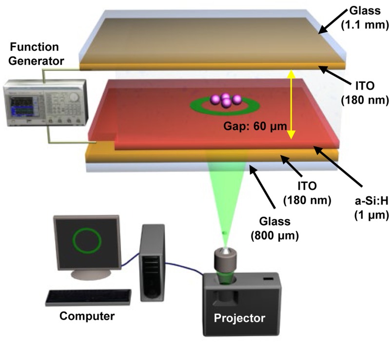
Figure 1 is a schematic illustration of a general OEK chip,92 which typically consists of four layers: a top glass layer coated with a transparent and conductive indiumtin oxide (ITO) film that is used as the top electrode for wiring the AC bias potential; a bottom glass layer with an ITO film that functions as the bottom electrode for connecting the other end of the AC bias potential; a thin film of photosensitive hydrogenated amorphous silicon (a-Si:H) deposited onto the bottom ITO glass layer; and a liquid layer fabricated by double-side adhesive tape between the a-Si:H layer and the top electrode to behave as a “gap” for the chip.
FIG. 1.
Schematic illustration of the OEK-based microfluidics system and experimental platform. Reproduced with permission from Liang et al., Sens. Actuators A Phys. 193, 103 (2013). Copyright 2013 Elsevier Publishing.
A commercial graphics software package (Adobe PremierePro CC2018, Adobe, USA) was used to produce the virtual electrodes, which illuminate the OEK chip via an LCD projector (VPL-F400X, Sony, Japan). To focus the optically-defined patterns, a condenser lens (MS plan, 50×, Nikon, Japan) was fixed between the LCD projector and the OEK chip. A high-speed and colorized CCD camera mounted on a microscope (Zoom 160, OPTEM, USA) was custom-designed to monitor the motion of suspended objects in real time. In addition, a function generator (Agilent 33522A, USA) was applied to provide a trigger voltage for exciting the OEK chip. The experimental setup was also described in detail with an actual photo.92
B. Fabrication of the OEK chip
The OEK chip was fabricated using a method that combines computer numerical control, CO2 laser microfabrication and the thin film technology and is hence suitable for mass fabrication at low costs.92 First, a 180 nm ± 10 nm ITO film was sputtered onto an 800-μm-thick glass substrate, and then a glass driller was used to form two through-holes with a diameter of approximately 1 mm. This type of ITO glass would serve as the top layer of the whole chip. Then, a 1-μm-thick a-Si:H was deposited onto the ITO glass surface without holes by plasma-enhanced chemical vapor deposition. The custom-designed microfluidic channel was mask-free and fabricated on double-sided adhesive tape (3M 9009, China) by a CO2 laser engraving machine (FL-570, Hengchunyuan Machinery Equipment Co. Ltd., China). To well wire the chip to the function generator, part of the a-Si:H layer must be uncovered. Thus, a 5 × 8 mm2 area of a-Si:H was etched to the ITO layer via standard photolithography and dry-etching enabled by the Oxford Plasma Lab 80 plasma etching system, with 2% oxygen, 12.5% CF4 gas, a 30 mTorr evacuated etching chamber, and 6-min plasma exposure.92 The chip was finally rinsed and cleaned with acetone and DI water and blown dry by N2 gas to keep its surface clean and dry for subsequent experiments.
C. Physical mechanism of OEK
Initially, no voltage is applied across the liquid layer without the incident light illuminating the chip. This is because nearly all the voltage is exerted onto the a-Si:H layer, which has a dark conductivity as low as 1 × 10⁻¹¹ S/m, about six-order lower than the most commonly used liquid solution in OEK chips. However, when the visible light image pattern with a power of 0.2 mW/cm2 is employed to illuminate the OEK chip and the photoconductivity of a-Si:H increases to 4 × 10⁻⁵ S/m, most of the voltage will shift to the liquid layer around the illumination area. Therefore, a nonuniform electric field is generated around the illumination area. The micro/nanoparticles and cells suspended in the OEK chip will be polarized by this optically-induced nonuniform electric field. Then, the interaction between the polarized objects and the nonuniform electric field will produce a DEP force exerted onto the objects, known as the optically-induced DEP (ODEP) force, which is defined as93
| (1) |
where R is the radius of the object, ɛ is the permittivity of the liquid, E is the electric field, rms means the root-mean-square value, the subscript m denotes the liquid, ω is the angular frequency, and K(ω) is the Clausius-Mossotti (CM) factor, which is further expressed as
| (2) |
In the above equation, ɛ* = ɛ–jσ/ω, where σ is the conductivity; ω = 2πf, where f is the applied voltage frequency across the liquid medium. The subscript p denotes the properties of the particle. The direction of the ODEP force, either positive or negative, is completely dictated by the real part of the CM factor. When the real part of the CM factor shows a sign higher than zero, a positive ODEP force will be generated and the objects will then be attracted to the illumination area. Otherwise, the objects will be pushed away from the illumination area. The theoretical finite element model (FEA) on this matter was discussed and described in 3D pictures.92,94
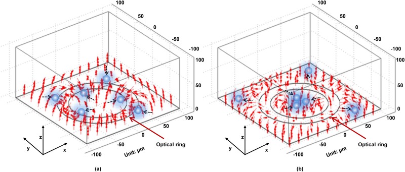
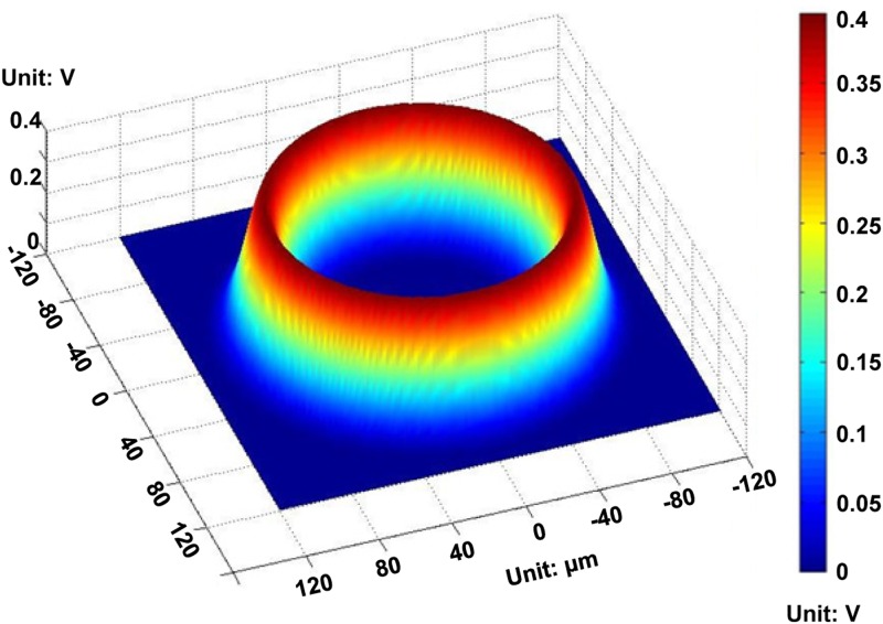
Figures 2(a) and 2(b) present the positive and negative ODEP forces generated by a ring pattern, respectively.92 The FEA results show how the two ODEP forces work and how the changed AC frequency leads objects of the same property to different locations. This establishes the theoretical basis that the method can be used to separate micro/nanoscaled particles and identify cells. In addition, the voltage distribution of the a-Si:H surface was obtained by using a ring pattern that acts as a virtual electrode,94 as shown in Fig. 3. The potential in the illumination area was much higher than that in other areas and its distribution can be described as a “trapping-potential well.”
FIG. 2.
Distribution of positive (a) and negative (b) ODEP forces by an optically-projected ring pattern. Reproduced with permission from Liang et al., Sens. Actuators A Phys. 193, 103 (2013). Copyright 2013 Elsevier Publishing.
FIG. 3.
Electric potential distribution of the a-Si:H surface. Reproduced with permission from Liang et al., Micromachines 3, 492 (2012). Copyright 2012 MDPI Publishing.
In addition, there indeed exist other forces in OEK chip, mainly including AC electroosmotic (ACEO) and AC electrothermal forces (ACET).66,92 Typically, when the applied AC frequency is lower than 10 kHz, then the optically-induced tangential electric field at the interface between the a-Si:H layer and the liquid chamber interacts with the double layer and produces a stable electrostatic force to act the boundary liquid and hence form a fluid flow at a slip velocity, which holds a same principle and revealed by utilizing the Helmholtz-Smoluchowski equation:95
| (3) |
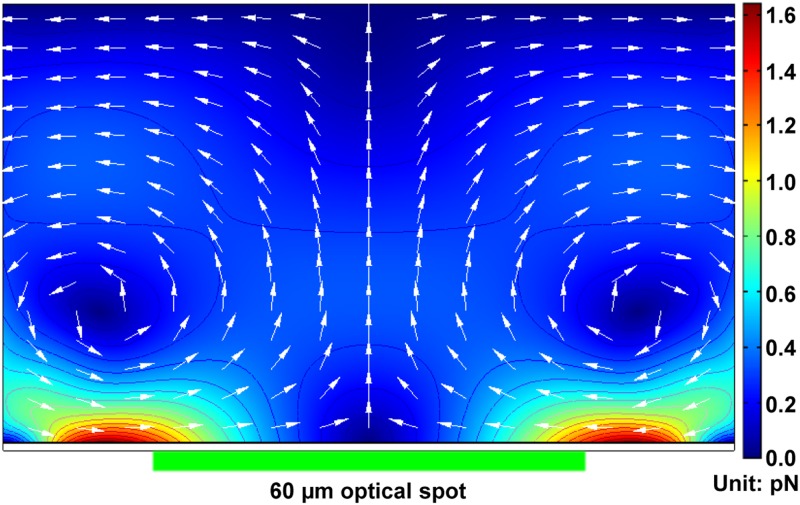
where ζ is the zeta potential of the electrical double layer, Et denotes the tangential electric field, and η is the dynamic viscosity of the liquid solution. The 2D spatial FEA results of the ACEO flow for various types of nanoscaled manipulations are shown in Fig. 4.96 The ACEO flow could push the suspended objects in the liquid chamber into the illumination center. Furthermore, the ACEO magnitude would decrease along the vertical direction from the a-Si:H surface and hence the manipulated and assembled objects would finally be concentrated and located at the a-Si:H surface.
FIG. 4.
FEA results of how the ACEO flow is spatially distributed in the OEK chip. The arrows and the surface color indicate the direction and magnitude of the ACEO force (unit: pN), respectively; the magnitude of the ACEO between any two adjacent isolines is 0.1 pN. Reproduced with permission from Liang et al., Opt. Mater. Express 4, 2368 (2014). Copyright 2014 OSA Publishing.
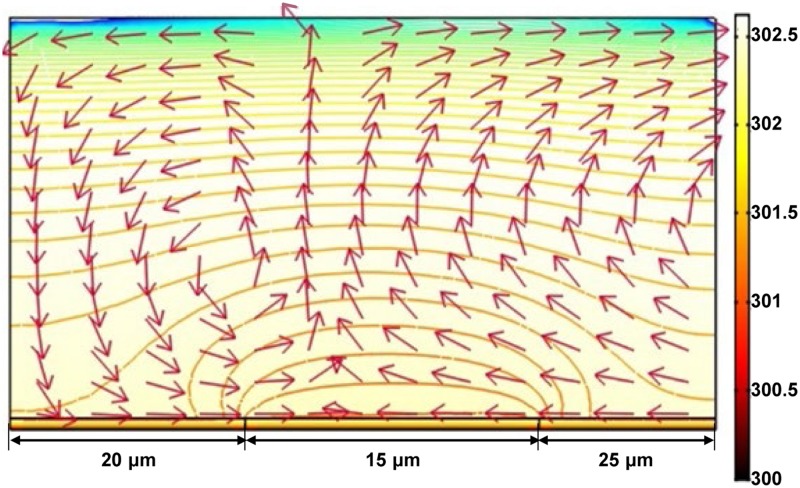
When the joule heating resulting from the optically-induced nonuniform electric field is exerted onto the liquid solution, a temperature gradient will occur and hence result in an electrothermal phenomenon called ACET in the OEK chip. The governing equations of ACET are expressed as95
| (4) |
where ρ is the density, the subscript f means the liquid solution, T is the temperature of the liquid solution, p is the pressure, V is the AC bias potential, and τ = ɛm/σm. For DI water at room temperature, approximately, k = 0.6 J m−1 s−1 K−1, ρm = 1 g⋅cm−3, α = −0.4% K−1, β = 2% K−1, ∂ρm/∂T/ρm = 10−4 K−1, and Cp = 4.184 kJ/kg/K.95
To get the numerical solution of ACET, we used a multiphysics FEA method to solve Eq. (4).97 Figure 5 shows the spatial distribution and magnitude of ACET. The temperature increased by ∼3 K, which was insignificant, and the temperature gradient was also rather low across the whole liquid chamber. In addition, the ACET flow could facilitate the positive ODEP-based manipulation from arrows in Fig. 5.
FIG. 5.
FEA results of how the ACET flow is spatially distributed in the OEK chip. The arrow and the surface color represent the direction of the ACET flow and the temperature distribution (unit: K) in the vertical direction of the OEK chip. The isolines represent the logarithmic distribution of the temperature gradient, with an interval value of 0.15 between any two adjacent isolines. Reproduced with permission from Liang et al., in 2011 IEEE International Conference on Nano/Micro Engineered and Molecular Systems (NEMS) (IEEE, 2011), p. 825. Copyright 2011 IEEE Publishing.
In addition, we experimentally and theoretically demonstrated that among the above-mentioned three different kinds of forces, ODEP was the dominant one when microscaled separation and manipulation was performed.92,94 However, when the OEK chip was utilized to manipulate gold nanoparticles, both of ACEO and ODEP assembled gold nanoparticles into microstructures and microelectrodes, which was also proved theoretically, respectively.96
D. Effects of the optical spectrum and electric field waveform on ODEP
As ODEP force is playing an increasingly important role in OEK-based manipulation, factors affecting the magnitude of ODEP force have become a focus of interest among researchers. Two major factors have been covered in related studies: optical spectrum and electric field waveform.94
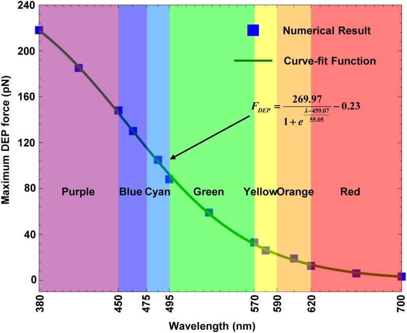
First, the absorption coefficient of a-Si:H increases nonlinearly as the wavelength of the visible light decreases.98,99 Based on this theory, the relationship between the optical spectrum’s wavelength and the magnitude of ODEP force was obtained when 10-μm-diameter polystyrene beads were selected as targets of interest. By using some typical values for each of the seven colors of visible light and referring to curve-fitting function, the solution of ODEP force and the wavelength was obtained, which was very close to the “numerical solution” and expressed as94
| (5) |
where λ is the wavelength of the light colors (unit: nm). Equation (5) is plotted in Fig. 6, from which we see that the magnitude of ODEP force decreases with increasing wavelength, and the purple light generates a higher ODEP force than all the other six colors of light. In addition, Eq. (5) satisfies the “Fermi-Dirac” function, which further proves that the electron-hole carrier generation phenomena exist in a-Si:H and the magnitude of ODEP force is highly dependent on the ability to excite the electron-hole. This theoretical result also offers a solid basis on how to select the projected optical color to optimize the experimental results using ODEP force.
FIG. 6.
Fitting results for maximum DEP force acting on a 10 μm polystyrene bead as a function of a different optical wavelength. Reproduced with permission from Liang et al., Micromachines 3, 492 (2012). Copyright 2012 MDPI Publishing.
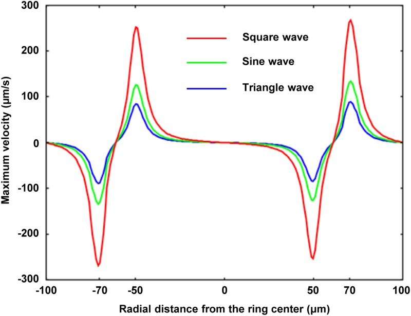
A sine wave function of AC bias potential is widely used in OEK-based applications and other electrorelated fields. We investigated which waveform could generate the maximum magnitude of ODEP force without changing the other input parameters.94 Specifically, a comparison was made between the sine function waveforms and the square and triangle waveforms that could be supplied by a conventional function generator with the same peak-to-peak voltage and frequency.94 Theoretically, the ratio of the magnitude of maximum velocity generated by the three waveforms was 6:3:2 based on the root-mean-square value of any periodical signal. Accordingly, a square waveform AC bias potential powering an OEK chip could produce twice and triple the magnitude of ODEP force than sine and triangle waveform AC bias potentials, respectively. The theoretical results were obtained by the FEA method, as shown in Fig. 7,94 and were experimentally validated.
FIG. 7.
FEA results of the maximum velocity induced by the ODEP force acting on a 10 μm polystyrene bead with respect to the square, sine, and triangle waveforms. Reproduced with permission from Liang et al., Micromachines 3, 492 (2012). Copyright 2012 MDPI Publishing.
III. OEK-BASED CELL AND MOLECULAR MANIPULATION AND APPLICATION
A. Cancer cell manipulation and separation
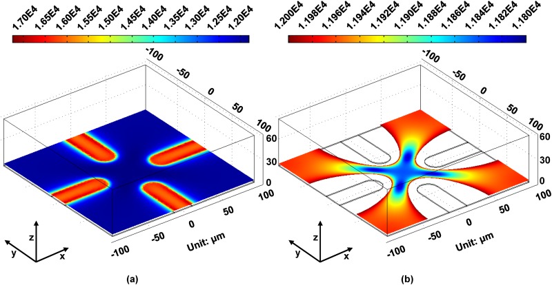
Noninvasive, cell-friendly, automatic, and rapid manipulation and separation of cells is the target of researchers. In our previous work, we presented an investigation on the self-rotational behavior of some types of cancer cells and red blood cells (RBCs) in an optically-induced nonuniform and nonrotational electric field.100–102 For instance, when the optical spot was defined and served as the virtual electrode driving the OEK chip, a nonuniform and axisymmetric electric field would be generated.101 Under this condition, Raji cells suspending in the OEK chip exhibited a self-rotational phenomenon, which was repeatable and controllable by the frequency and voltage of an externally applied AC bias potential. In addition, the self-rotation speed of Raji cells reached its maximum at a frequency of 60 kHz. The curve-fitting function of the self-rotation speed of Raji cells demonstrated a Gaussian distribution with the frequency and a quadratic relationship with the applied voltage, respectively. To experimentally observe the areas where the Raji cells could self-rotate, four orthogonal electrodes were custom-designed to manipulate the cells, followed by FEA modeling of the spatial distribution of the optically-induced electric field (Fig. 8). Figure 8(a) shows the distribution of the optically-induced electric field, and Fig. 8(b) clearly presents the local electric field distribution of Fig. 8(a), which elucidated the nonuniform electric field distribution in the central area of the four orthogonal optical patterns. The experimental and theoretical results validated that the nonuniform electric field would play a pivotal role in the self-rotation of the cells.
FIG. 8.
FEA results of the distribution of the optically-induced electric field. (a) Distribution of the electric field induced by four orthogonal optical patterns; (b) the local electric field distribution at the central areas, showing the uniform electric field in blue. Reproduced with permission from Liang et al., Biomicrofluidics 9, 014121 (2015). Copyright 2015 AIP Publishing LLC.
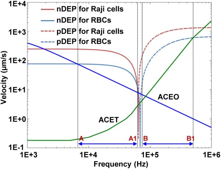
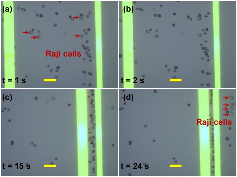
Label-free separation of cells has long been a focus of interest in biorelated researches and applications. A noninvasion approach was proposed to characterize label-free separation of Raji cells from RBCs.103 Typically, there are many RBCs in an extracted sample of Raji cells. Thus, it is required to identify and purify the Raji cells in a mixed cell population that may affect subsequent detection and research protocols. For this purpose, we investigated the possibility of discriminating Raji cells from RBCs using ODEP. The shell-core polarization models of Raji cells and RBCs were employed to characterize the electrical properties of the optically-induced nonuniform field. This established the theoretical basis that Raji cells could be separated from RBCs using the ODEP force of different magnitudes due to their different dielectric properties and sizes. An FEA simulation of the OEK forces acting on the two types of cells was carried out to get the frequency range of the dominant ODEP force as shown in Fig. 9. The results showed that a frequency in the range of ∼7–60 kHz, which includes a negative ODEP force, is more suitable for conducting the separation experiments. This is because the ACET force in this frequency range is much lower, which means a lower heat effect and thus less impacts on the cellular properties. Figure 10 shows an example of the separation of Raji cells from RBCs with a concentration ratio of 1:10, proving that these two types of cells could be successfully separated with an experimental process.
FIG. 9.
OEK forces on the velocities for Raji cells and RBCs vs the applied frequency. Reproduced with permission from Liang et al., PloS One 9, e90827 (2014). Copyright 2014 PLoS Publishing.
FIG. 10.
Separation of Raji cells from RBCs with a concentration ratio of 1:10. (a) Initially, when the optical patterns were projected onto the a-Si:H surface without externally applied voltage, both of Raji cells and RBCs were suspended in the liquid solution; (b) when the voltage was switched on, the two types of cells were repelled; (c) the 25 μm-wide optical line was set with a translational velocity of 12 μm/s from left to right and the 15 μm-optical line was kept static. After 15-s movement of 25 μm-wide optical line, the two types of cells were aligned between the gap of the two lines; (d) the Raji cells were separated from RBCs. Reproduced with permission from Liang et al., PloS One 9, e90827 (2014). Copyright 2014 PLoS Publishing.
Moreover, a dynamic response-based cell separation scheme was proposed.104 Raji cells and RBCs were experimentally found to show different initial velocities when an AC bias potential was switched on and the optically-projected line illuminated the chip. This finding was theoretically validated by exploring the first-order transit movement response of cells under an ODEP force field. This transit motion was described with an analysis of time dependent acceleration and velocity. In general, the Stoke drag force was considered to balance the ODEP force. However, if the time domain for the velocity and acceleration of cell transit were not neglected, then the acceleration factor should be considered. The following formula was derived to reflect this dynamic response:104
| (6) |
where m is the cell mass, τ and U0 are the time constant parameters, and η is the dynamic viscosity of cells in the fluidic medium. Equation (6) shows that the dynamic response of cells is independent of their position, but associated with their intrinsic properties. This explains why they show different initial velocities and accelerations. This theory was further proven by an experimental process, which involved a computer-vision based analysis of the dynamic motion of Raji cells and RBCs.
B. Isolation of circulating tumor cells
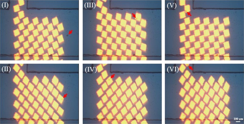
CTCs in larger populations or clusters play a more critical role in cancer metastasis than individual CTCs. Wu et al. utilized ODEP to isolate CTC clusters from leukocytes with a cell purity as high as 91.5 ± 5.6%.105 They proposed a two-step ODEP-based cell manipulation: CTCs were primitively isolated and concentrated by a dynamic array of rotational square light patterns in a T-shaped microchannel, as shown in Fig. 11.
FIG. 11.
ODEP-based isolation of CTC clusters. (I) and (II) A dynamic square light image trapped a cell cluster (red arrow) passing through the incident optical pattern; (II) and (III) the trapped cell cluster moved to one side of main microchannel; (III)–(V) the cell cluster was trapped again at the entrance of side microchannel; (V) and (VI) the trapped cancer cell cluster was pushed into the side microchannel for collection. Reproduced with permission from Chiu et al., Sens. Actuators B Chem. 258, 1161 (2018). Copyright 2018 Elsevier Publishing.
The separation scheme was based on the significant diameter difference between CTCs and leukocytes. Subsequently, CTCs were located at the junction areas in the microchannel and the leukocytes were flushed and directed toward the waste outlet. Furthermore, the isolated CTCs were moved and delivered into the side microchannel for secondary purification. Above all, the resulting recovery rate reached 70.5 ± 5.2% without compromising the CTCs’ integrity and bioproperties. They also experimentally optimized ODEP operating parameters, including electrical conditions, microfluidic elements, and optical geometries. This study has enabled new applications of ODEP for concentrating and isolating CTCs and other kinds of cells.
C. Manipulation of single DNA molecules
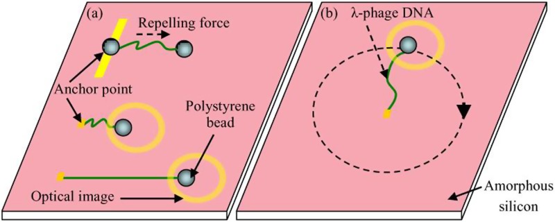
Manipulation of single DNA molecules has received attention from researchers in biological and nanotechnological fields. It is envisioned that the ability to stretch a single DNA molecule will yield intrinsically the mechanical properties of DNA. Indirect and real-time elongation and rotation of a single DNA molecule was investigated with the aid of microbeads utilizing an ODEP force.106 One end of the DNA molecule was chemically modified and anchored onto the substrate of an OEK chip, and the other end was attached onto a microbead. Then, by moving the optically-projected pattern away from the anchor point of the DNA molecule, the DNA molecule was stretched, as schematically shown in Fig. 12(a). If the virtual electrode was set to rotate around the anchor point of the DNA molecule, then the DNA molecule would correspondingly follow a consistent rotational action, which is depicted in Fig. 12(b). By using a fluorescent dye and an oxygen scavenging buffer, real-time observation of how a single DNA molecule is elongated was achieved, as shown in Fig. 13. Characterization results showed that a maximum of 61.3 pN ODEP force could be exerted onto the DNA molecule.
FIG. 12.
Manipulation of a single DNA molecule. (a) Stretching and (b) rotation of a single DNA molecule. Reproduced with permission from Lin et al., Opt. Express 17, 15318 (2009). Copyright 2009 OSA Publishing.
FIG. 13.
Elongation of a single DNA molecule through the interaction between the microbead and the optical image. (a) A DNA molecule was treated with one end bound to a microbead and the other end with the substrate; (b) the generated negative ODEP force was employed to trap the microbead; (c) and (d) by moving the trapped microbead with the aid of computer software, a single DNA molecule was successfully stretched to a programmed position. Reproduced with permission from Lin et al., Opt. Express 17, 15318 (2009). Copyright 2009 OSA Publishing.
IV. OEK-BASED BIOMEDICAL AND BIOENGINEERING APPLICATIONS
A. Patterning hydrogels for cell patterning and tissue engineering
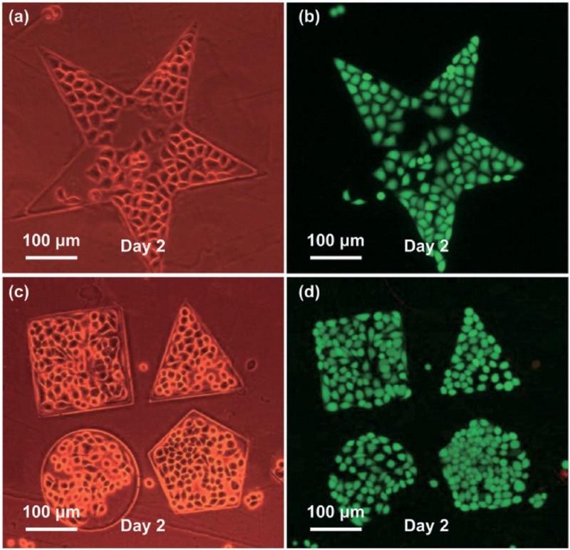
The extracellular microenvironment has both positive and negative impacts on cell growth and other cellular behaviors. A novel non-UV-based method was, therefore, developed by our group to pattern cancer cells.107 First, we fabricated poly(ethylene glycol) diacrylate (PEGDA)-based hydrogel microstructures using optically-projected images in an OEK chip. Then, we patterned lines, circles, pentagons, and other complex shapes in the hydrogel with a line resolution of lower than 3 μm and a thickness of up to 6 μm within 8 s. Without using any masks, the whole experimental process was completed by simply tuning the computer-controlled digital light images. Afterwards, the upper ITO layer was removed to expose the fabricated hydrogel microstructures, and then, the subsequent OEK chip was loaded into the culture medium to culture MCF-7 cells on an OEK chip for two days. Results showed that cells adhered to the bare a-Si:H areas but not to the hydrogel areas. Five different cell patterns are presented in Fig. 14. The fluorescent images after culturing for two days validated that this method can culture cells with good viability while being noninvasive to the cells.
FIG. 14.
(a) and (c) show the microscope images of patterning MCF-7 cells in confined PEGDA microstructures by a phase difference mode; (b) and (d) are the fluorescent images of (a) and (c), respectively, where viable cells are stained in green and the dead ones in red. Reproduced with permission from Liu et al., Lab Chip 14, 1367 (2014). Copyright 2014 RSC Publishing.
In addition, our group went beyond 2D views to pattern cells in 3D views.108 A layer-by-layer approach to forming 3D PEGDA-based microstructures was successfully demonstrated.109 A theoretical explanation of the mechanism of this approach was provided to explain the polymerization reaction and the formation process of 3D hydrogel structures. After that, a large area of hydrogels was created by a series of dynamically modified images, including a stereoscopic meshlike microstructure network with intersecting hydrogel microbelts and tunable pores and gaps of the network. By further cell culturing and tissue engineering, these microstructures have been demonstrated to be capable of functioning as 3D biomodels.
B. Determination of cell dielectric parameters
A cell’s intrinsic properties can be an indicator of its function and state. Cell membrane capacitance and conductance are two key types of cellular biophysical properties that have been used as electrophysiological biomarkers to assess cellular phenotype and state. These parameters have many associated clinical applications. A method that uses an OEK chip to determine cell membrane capacitance and conductance was proposed.110 The changed frequency applied into the OEK chip could generate a positive or negative ODEP force to be experienced by the cells, which resulted in two different cell directions relative to the illumination area. The critical frequency that led the ODEP force motion to shift from positive to negative or vice versa (i.e., Re[K(ω)] = 0) was defined as the crossover frequency of cells. In this case, the relationship between cell membrane and conductance and external parameters that could be measured experimentally (liquid conductivity, crossover frequency of cells and curve-fitting information) was derived and expressed as110
| (7) |
where Cmem and Gmem are cell membrane capacitance and conductance, respectively. It was clearly seen that the crossover frequency of cells would increase linearly with respect to the liquid conductivity with a slope and a fcrossover-axis intercept. Hence, cell membrane and conductance could be further derived and expressed as106
| (8) |
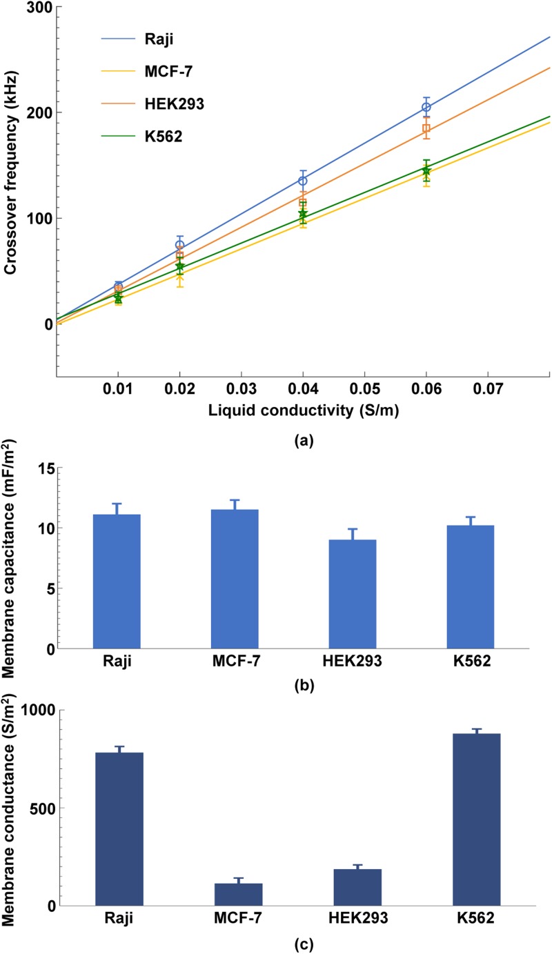
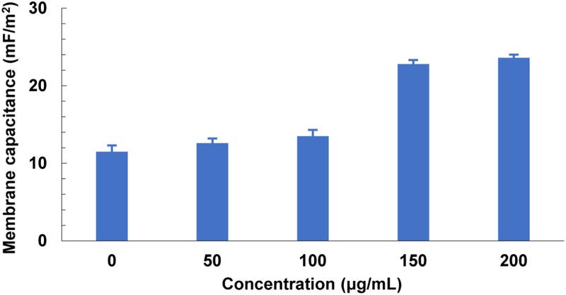
Using a self-developed image matching algorithm, our group conducted a series of experiments to extract the membrane capacitance and conductance of four types of cancer cells and thereby to identify cellular translational motions rapidly and accurately.111 Figure 15 shows the determination process and results of cellular membrane capacitance and conductance of four different kinds of cells. Results in Fig. 15(a) revealed that the measured crossover frequencies of four different kinds of cells vs liquid conductivities held a linear relationship. By referring to Eq. (8), cell membrane capacitance and conductance were extracted, as shown in Figs. 15(b) and 15(c), respectively. The effectiveness of this method was demonstrated by a comparison between the cell parameters between the method proposed in Ref. 110 and those presented in other works. In addition, the concentration of resveratrol applied to MCF-7 cells was investigated by extracting the cell membrane capacitance. Results in Fig. 16 indicated that the membrane capacitance of MCF-7 cells in a drug-free medium was always lower than that of MCF-7 cells treated by drug solutions. Furthermore, an increase in the drug concentration also resulted in an increase in the cell membrane capacitance.
FIG. 15.
(a) Experimentally-obtained crossover frequencies for four different kinds of cells as a function of liquid conductivities; extracted membrane capacitance (b) and conductance (c) of four different kinds of cells. Reproduced with permission from Liang et al., Biophys. J. 113, 1531 (2017). Copyright 2017 Elsevier Publishing.
FIG. 16.
Extracted membrane capacitance of MCF-7 cells with respect to drugs of four different concentrations. Reproduced with permission from Liang et al., Biophys. J. 113, 1531 (2017). Copyright 2017 Elsevier Publishing.
C. Determination of cell mass and density
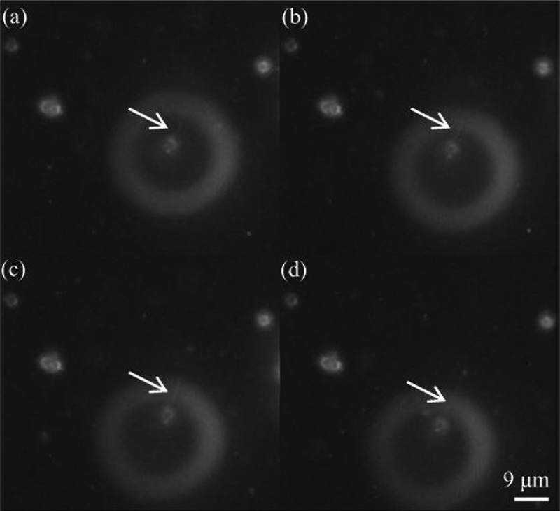
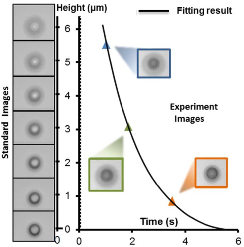
A technique that combines sedimentation theory and computer vision in an OEK chip was proposed to determine the mass and density of single cells.112,113 Basically, a negative ODEP force allowed the micro/nano-objects to be lifted from the a-Si:H surface up to a certain height. Then, as the height increased, the magnitude of the negative ODEP force would decrease sharply to approximately zero, and the manipulated objects will “free fall” down to the a-Si:H surface under the competing buoyant, gravitational, and Stoke’s drag forces. In theory, the density and mass of micro/nano-objects can be indirectly determined by cell force and trajectory analysis. By using the computer-vision technique, the trajectory of the micro/nano objects was extracted from the captured experimental image sequences to accurately reflect the motion of these objects in the liquid solution. A polystyrene bead with a known mass and density was first tested to validate the accuracy and validity of the proposed method, as shown in Fig. 17. After that, the mass and density of yeast112 and leukemic cells113 were determined successfully.
FIG. 17.
Comparison between the standard images of a polystyrene bead and a dynamically moving bead at different heights to extract their motion with time. Reproduced with permission from Zhao et al., Lab Chip 14, 4426 (2014). Copyright 2014 RSC Publishing.
Moreover, a precise, safe, and user-friendly method that uses ODEP-facilitated electroporation in an OEK chip to transfect multiple DNA transfection was developed.114 A low AC voltage (13 Vpp) was enabled to selectively allow cells of interest to be electroporated without killing the cells and hence facilitate the subsequent DNA transfection. The optically-induced nonuniform electric field generated a potential exerted onto the cell membrane, thereby producing transit pores in the cell membrane. Accordingly, the entry path of exogenous DNA plasmids could be created. Fluorescent DNA plasmids were successfully transfected into a variety of mammalian cells. Then, the gene transfection efficiency was theoretically and experimentally optimized based on the exposure time and optically-projected patterns. Fluorescent proteins were also observed in live transfected cells to further prove the viability of this method.
D. ODEP-based cell fusion and drug resistance research
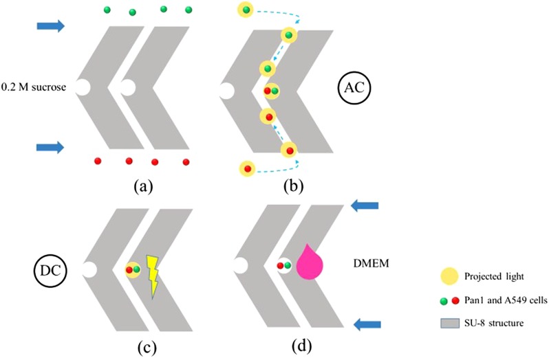
To enable cell pairing at high efficiencies and yields, a method featuring the use of ODEP and an optically-activated electric field on a custom-designed microfluidic microstructure was developed for accurate and automatic cell pairing.115,116 Figure 18 is a schematic illustration of the cell manipulation process. SU-8 chevron-shaped microstructures were designed to facilitate cell paring and prevent the cells from diffusing before entering into reservoirs (“notches” in the center of the microstructures). First, two different types of cells were injected into the chip via two different inlets, as shown in Fig. 18(a). Then, the cells were moved into reservoirs [Fig. 18(b)] by ODEP with an AC bias potential. After cell pairing, DC pulses were utilized to produce a transmembrane potential across the cellular membrane without killing the cells [Fig. 18(c)]. In this way, the cells were electroporated and a cell fusion process was finally triggered. Furthermore, a cell culture medium was added for on-chip cellular culture, as shown in Fig. 18(d). This has demonstrated that OEK can be a promising technology for the automatic fusion of different types of cells and other biomedical applications.
FIG. 18.
Schematic illustration of experimental procedures of cell fusion. (a) Cells were loaded into the inlets and moved into the upper and lower microchannels due to hydraulic pressure differences; (b) cells were paired by the projected white light; (c) electric pulses were applied to trigger cell fusion; (d) after fusion, culture media were injected into each outlet chamber for on-chip cell culture. Reproduced with permission from Hsiao et al., Biomicrofluidics 12, 034108 (2018). Copyright 2018 AIP Publishing LLC.
The heterogeneity of cancer cells in a tumor is a key cause of drug resistance and thereby failure in clinical diagnosis and treatment. An ODEP-based technique was proposed to explore the drug resistance of cancer cells.117 This technique operates on a principle that different levels of viability and drug resistance of cancer cells lead to diversity in conductivity and thus ODEP forces of varying magnitude and direction. By exerting different ODEP forces onto the cells, both different types of cancer cells and the same type of cell with different levels of viability and anticancer drug resistance gene expression were successfully separated. This technique has offered a new angle to understand the heterogeneity of cancer cells with respect to their anticancer drug resistance and further facilitate fundamental studies in the biomedical field.
V. CHALLENGES AND PROSPECTS
As reviewed in this paper, the OEK technique has offered tremendous research benefits to the microfluidics community, while playing an increasing role in material/biorelated applications. Most OEK-based studies to date focused on (1) the manipulation, assembly, and synthesis of micro/nanoscaled materials, (2) the manipulation, separation, and identification of single cells/molecules, and (3) the acquisition of the intrinsic bioinformation of cells. These works have clearly demonstrated the unique versatility and flexibility of the OEK technique. However, if technology has little potential for real-world applications, it will be of limited value and ultimately become neglected. Consequently, a list of challenges must be addressed for this technique to mature from the lab experiments to real-world applications. Below is a brief discussion of the major challenges facing the OEK technique and a few prospects about making it more applicable and useful.
Integration with other microfluidic elements and micro/nanorobotics will be the first thing to consider. OEK allows us to flexibly and automatically manipulate, assemble, and separate micro/nanomaterials/cells without using any metal electrode or high-power optical input. In the early days of OEK, 2D manipulation brought great convenience to researchers. Although a two-layer photoconductive material-based OEK chip was demonstrated to be potentially able to realize 3D manipulation of beads,118 its applications were limited due to the relatively low light transmission and poor fusion performance generated by conventional microfluidic components. As this method evolves over time, researchers have recognized the importance of integrating OEK with other devices/tools to detect, analyze, and measure micro/nano-objects for biomedical and tissue engineering applications. This requires systematically combining OEK chips with other predominant micro/nanorobotic-based techniques, such as atomic force microscopy,119 acoustics tweezers,120 and scanning ion conductance microscopy,121 to achieve efficient 3D manipulation and multiparameter simultaneous acquisition, detection, and analysis of single cells.
In addition, more studies need to be carried out to explore the underlying mechanisms of cellular motion under various conditions. Currently, our group has shown the self-rotation of certain types of single cancer cells and individual RBCs in an OEK chip.100–102 However, there has yet to be any theoretical model explaining why only some types of cells have this special self-rotation phenomenon in an optically-induced nonrotational electric field. Recently, a model for the self-rotation of cells in a DEP field was reported and experimentally validated.122–124 Nevertheless, it did not reveal the correlation between the intrinsic properties of cells and nonuniform and nonrotational fields. Also, although both a DEP and an ODEP field rely on a nonuniform electric field, an ODEP field generally relies on a much more nonuniform electric field than a DEP field, which can be seen from our previous simulation results.101–104 Hence, an ODEP field exhibits a higher cell polarization level, which warrants a more complex self-rotation model for theoretically analyzing the observed experimental phenomenon. Main OEK forces including ODEP, ACEO, and ACET as well as the buoyant force and Brownian motion have been extensively studied and reported. Optically-induced electrodeposition was also demonstrated. However, a more complex and accurate model that combines all forces and mechanisms and can describe the behaviors of micro/nano-objects and fluid flows is still absent. Therefore, current OEK-based manipulation techniques are still highly limited in terms of resolution and automation.
New candidate materials and manipulation schemes should also be explored. The effectiveness of the OEK-based manipulation technique is highly dependent on the photoconductive material used on fabricating the OEK chip. To date, a-Si:H is one of the mostly used materials for fabricating OEK chips26,77,80 due to its high stability, ease of fabrication, good light transmittance and adsorption, and reusability. Lithium niobate crystal was recently demonstrated to behave as a photoconductive material for generating an optically-induced nonuniform field that can easily bond with PDMS.125,126 Most importantly, this nonuniform field can remain permanent even when the optically-projected images are removed. However, this technique offers limited manipulation resolution and an OEK chip based on this material can only be used as a 2D manipulation method. In addition, the key capabilities of an OEK chip have already been demonstrated to include assembly, separation, trapping, concentration, fabrication, translation, self-rotation, and synthesis of micro/nano-objects. It is, therefore, possible to explore the simultaneous combination of two or more of these capabilities to allow new applications in materials science and biorelated fields.
Finally, even more efforts should be put to extend the applicability of the OEK technique. Validating its real benefits and practical applications should be a long-term goal. The past decade has witnessed the evolvement of the OEK technique from manipulation and synthesis of micro/nanomaterials to biomedical and bioengineering applications. Compared to other micro/nanomanipulation technologies such as optical tweezers, an OEK-based technique can manipulate micro/nano-objects with a much smaller optical power and requires no fabrication of metal electrodes. However, these advantages do not make the OEK-based microfluidic technology a complete replacement for other technologies. One example of expanding the application of OEK technology is in the currently popular 3D tissue engineering field.127–129 OEK-based technology has already demonstrated 3D fabrication of hydrogel-based bioscaffolds;108 however, the scaffolds have limited applicability in tissue engineering due to the limited geometries of microstructures that can be fabricated using OEK due to the lack of precise control of OEK phenomena in a microfluidic environment.
Since its advent in 2005, the OEK technique has been explored by world-wide researchers in various fields. However, the current results suggest that OEK-based lab-on-a-chip systems can only benefit laboratory research and are far away from being accepted by end users and industries for commercialization. Hence, if the above-mentioned challenges can be overcome, OEK-based devices will be able to move away from being lab-oriented technologies and become widely used in real-world applications.
ACKNOWLEDGMENTS
This work was supported by the National Natural Science Foundation of China (Project Nos. 61973224 and 61803088), the Natural Science Foundation of Liaoning Province (Project No. 2019-KF-01-15), and the Scientific Research Innovation Cultivation Project of Shenyang Jianzhu University (Project No. CXPY2017012). Wen Jung Li would also thank the support from the Hong Kong Research Grants Council (Project Nos. 9042639 and 907002) and the Joint NSFC/RGC Scheme (Project No. CityU132/14).
Contributor Information
Lianqing Liu, Email: .
Wen Jung Li, Email: .
REFERENCES
- 1.Kolluri N., Klapperich C. M., and Cabodi M., Lab Chip 18, 75 (2018). 10.1039/C7LC00758B [DOI] [PubMed] [Google Scholar]
- 2.Mobini S., Song Y. H., McCrary M. W., and Schmidt C. E., Biomaterials 198, 146 (2019). 10.1016/j.biomaterials.2018.05.012 [DOI] [PMC free article] [PubMed] [Google Scholar]
- 3.Li X., Soler M., Özdemir C. I., Belushkin A., Yesilköy F., and Altug H., Lab Chip 17, 2208 (2017). 10.1039/C7LC00277G [DOI] [PubMed] [Google Scholar]
- 4.Ouyang M., Cheung W. K., Liang W., Mai J. D., Liu W. K., and Li W. J., Biomicrofluidics 7, 054112 (2013). 10.1063/1.4821169 [DOI] [PMC free article] [PubMed] [Google Scholar]
- 5.Chung J., Hwang H. Y., Chen Y., and Lee T. Y., Sens. Actuators B Chem. 254, 542 (2018). 10.1016/j.snb.2017.07.122 [DOI] [Google Scholar]
- 6.Dittrich P. S. and Manz A., Nat. Rev. Drug Discov. 5, 210 (2006). 10.1038/nrd1985 [DOI] [PubMed] [Google Scholar]
- 7.Rodriguez N. M., Wong W. S., Liu L., Dewar R., and Klapperich C. M., Lab Chip 16, 753 (2016). 10.1039/C5LC01392E [DOI] [PMC free article] [PubMed] [Google Scholar]
- 8.Hur S. C., Henderson-MacLennan N. K., McCabe E. R. B., and Carlo D. D., Lab Chip 11, 912 (2011). 10.1039/c0lc00595a [DOI] [PubMed] [Google Scholar]
- 9.Ni M., Tresset G., and Iliescu C., Sens. Actuators B Chem. 252, 458 (2017). 10.1016/j.snb.2017.06.028 [DOI] [Google Scholar]
- 10.Chen W. T., Lin G. B., Lin S. H., Lu C.-H., Hsieh C.-H., Ma B.-L., and Chao C.-Y., PLoS One 13, e0191078 (2018). 10.1371/journal.pone.0191078 [DOI] [PMC free article] [PubMed] [Google Scholar]
- 11.Snezhko A. and Aranson I. S., Nat. Mater. 10, 698 (2011). 10.1038/nmat3083 [DOI] [PubMed] [Google Scholar]
- 12.Liu H. L., Shi Y., Liang L., Li L., Guo S. S., Yin L., and Yang Y., Lab Chip 17, 1280 (2017). 10.1039/C7LC00078B [DOI] [PubMed] [Google Scholar]
- 13.Lee W. K., Dai Z., King W. P., and Sheehan P. E., Nano Lett. 10, 129 (2009). 10.1021/nl9030456 [DOI] [PubMed] [Google Scholar]
- 14.Wang K., Zhou W., Lin Z., Cai F., Li F., Wu J., Meng L., Niu L., and Zheng H., Sens. Actuators B Chem. 258, 1174 (2018). 10.1016/j.snb.2017.12.013 [DOI] [Google Scholar]
- 15.Mao Z., Li P., Wu M., Bachman H., Mesyngier N., Guo X., Liu S., Costanzo F., and Huang T. J., ACS Nano 11, 603 (2017). 10.1021/acsnano.6b06784 [DOI] [PMC free article] [PubMed] [Google Scholar]
- 16.Cross S. E., Jin Y. S., Rao J., and Gimzewski J. K., Nat. Nanotechnol. 2, 780 (2007). 10.1038/nnano.2007.388 [DOI] [PubMed] [Google Scholar]
- 17.Kim S., Shafiei F., Ratchford D., and Li X., Nanotechnology 22, 115301 (2011). 10.1088/0957-4484/22/11/115301 [DOI] [PubMed] [Google Scholar]
- 18.Li X., Liu C., Chen S., Wang Y., Cheng S. H., and Sun D., IEEE Trans. Robot. 33, 1200 (2017). 10.1109/TRO.2017.2718554 [DOI] [Google Scholar]
- 19.Kirch J., Schneider A., Abou B., Hopf A., Schaefer U. F., Schneider M., Schall C., Wagner C., and Lehr C.-M., Proc. Natl. Acad. Sci. U.S.A. 109, 18355 (2012). 10.1073/pnas.1214066109 [DOI] [PMC free article] [PubMed] [Google Scholar]
- 20.Ouyang M., Hill W., Lee J. H., and Hur S. C., Sci. Rep. 7, 44757 (2017). 10.1038/srep44757 [DOI] [PMC free article] [PubMed] [Google Scholar]
- 21.Fung C. K. M., Wong V. T. S., Chan R. H. M., and Li W. J., IEEE Trans. Nanotechnol. 3, 395 (2004). 10.1109/TNANO.2004.834156 [DOI] [Google Scholar]
- 22.Wu M., Mao Z., Chen K., Bachman H., Chen Y., Rufo J., Ren L., Li P., Wang L., and Huang T. J., Adv. Funct. Mater. 27, 1606039 (2017). 10.1002/adfm.201606039 [DOI] [PMC free article] [PubMed] [Google Scholar]
- 23.Kwak B., Lee J., Lee D., Lee K., Kwon O., Kang S., and Kim Y., Biosens. Bioelectron. 88, 153 (2017). 10.1016/j.bios.2016.08.002 [DOI] [PubMed] [Google Scholar]
- 24.Hampson S. M., Rowe W., Christie S. D. R., and Platt M., Sens. Actuators B Chem. 256, 1030 (2018). 10.1016/j.snb.2017.10.041 [DOI] [Google Scholar]
- 25.Zhang J., Yuan D., Zhao Q., Yan S., Tang S.-Y., Tan S. H., Guo J., Xia H., Nguyen N.-T., and Li W., Sens. Actuators B Chem. 267, 14 (2018). 10.1016/j.snb.2018.04.020 [DOI] [Google Scholar]
- 26.Chiou P.-Y., Ohta A. T., and Wu M. C., Nature 436, 370 (2005). 10.1038/nature03831 [DOI] [PubMed] [Google Scholar]
- 27.Jamshidi A., Pauzauskie P. J., Schuck P. J., Ohta A. T., Chiou P.-Y., Chou J., Yang P., and Wu M. C., Nat. Photonics 2, 86 (2008). 10.1038/nphoton.2007.277 [DOI] [PMC free article] [PubMed] [Google Scholar]
- 28.Wu M. C., Nat. Photonics 5, 322 (2011). 10.1038/nphoton.2011.98 [DOI] [Google Scholar]
- 29.Choi W., Kim S. H., Jang J., and Park J.-K., Microfluid. Nanofluid. 3, 217 (2007). 10.1007/s10404-006-0124-5 [DOI] [Google Scholar]
- 30.Pauzauskie P. J., Jamshidi A., Valley J. K., J. H. Satcher, Jr., and Wu M. C., Appl. Phys. Lett. 95, 113104 (2009). 10.1063/1.3212725 [DOI] [PMC free article] [PubMed] [Google Scholar]
- 31.Lee M. W., Lin Y. H., and Lee G.-B., Microfluid. Nanofluid. 8, 609 (2010). 10.1007/s10404-009-0492-8 [DOI] [Google Scholar]
- 32.Hwang H. and Park J. K., Anal. Chem. 81, 5865 (2009). 10.1021/ac901047v [DOI] [PubMed] [Google Scholar]
- 33.Hwang H., Han D., Oh Y. J., Cho Y.-K., Jeong K.-H., and Park J.-K., Lab Chip 11, 2518 (2011). 10.1039/c1lc20277d [DOI] [PubMed] [Google Scholar]
- 34.Hu W., Ishii K. S., Fan Q., and Ohta A. T., Lab Chip 12, 3821 (2012). 10.1039/c2lc40483d [DOI] [PubMed] [Google Scholar]
- 35.Han D., Hwang H., and Park J. K., Appl. Phys. Lett. 102, 054105 (2013). 10.1063/1.4790622 [DOI] [Google Scholar]
- 36.Hwang H. and Park J. K., Anal. Chem. 81, 9163 (2009). 10.1021/ac9021709 [DOI] [PubMed] [Google Scholar]
- 37.Zhang S., Juvert J., Cooper J. M., and Neale S. L., Sci. Rep. 6, 32840 (2016). 10.1038/srep32840 [DOI] [PMC free article] [PubMed] [Google Scholar]
- 38.Han D. and Park J. K., Lab Chip 16, 1189 (2016). 10.1039/C6LC00110F [DOI] [PubMed] [Google Scholar]
- 39.Han D. and Park J. K., Biomicrofluidics 10, 034106 (2016). 10.1063/1.4950787 [DOI] [PMC free article] [PubMed] [Google Scholar]
- 40.Ke L. Y., Kuo Z. K., Chen Y. S., Yeh T.-Y., Dong M., Tseng H.-W., and Liu C.-H., Lab Chip 18, 106 (2018). 10.1039/C7LC00963A [DOI] [PubMed] [Google Scholar]
- 41.Kamata M., Taguchi Y., and Nagasaka Y., Opt. Express 26, 16970 (2018). 10.1364/OE.26.016970 [DOI] [PubMed] [Google Scholar]
- 42.Lim M. B., Felsted R. G., Zhou X., Smith B. E., and Pauzauskie P. J., Appl. Phys. Lett. 113, 031106 (2018). 10.1063/1.5025225 [DOI] [Google Scholar]
- 43.Kremer C., Witte C., Neale S. L., Reboud J., Barrett M. P., and Cooper J. M., Angew. Chem. 126, 861 (2014). 10.1002/ange.201307751 [DOI] [PMC free article] [PubMed] [Google Scholar]
- 44.Witte C., Kremer C., Chanasakulniyom M., Reboud J., Wilson R., Cooper J. M., and Neale S. L., Small 10, 3026 (2014). 10.1002/smll.201400247 [DOI] [PubMed] [Google Scholar]
- 45.Gi H. J., Han D., and Park J. K., Biofabrication 9, 015011 (2017). 10.1088/1758-5090/aa564c [DOI] [PubMed] [Google Scholar]
- 46.Huang S. H., Hung L. Y., and Lee G.-B., Lab Chip 16, 1447 (2016). 10.1039/C5LC01284H [DOI] [PubMed] [Google Scholar]
- 47.Ohta A. T., Chiou P. Y., Phan H. L., Sherwood S. W., Yang J. M., Lau A. N. K., Hsu H., Jamshidi A., and Wu M. C., IEEE J. Sel. Top. Quant. Electron. 13, 235 (2007). 10.1109/JSTQE.2007.893558 [DOI] [Google Scholar]
- 48.Lau A. N. K., Ohta A. T., Phan H. L., Hsu H.-Y., Jamshidi A., Chiou P.-Y., and Wu M. C., Lab Chip 9, 2952 (2009). 10.1039/b907840a [DOI] [PubMed] [Google Scholar]
- 49.Wang S., Liang W., Dong Z., Lee G.-B., and Li W. J., Micromachines 2, 431 (2011). 10.3390/mi2040431 [DOI] [Google Scholar]
- 50.Ohta A. T., Jamshidi A., Valley J. K., Hsu H.-Y., and Wu M. C., Appl. Phys. Lett. 91, 074103 (2007). 10.1063/1.2771091 [DOI] [PMC free article] [PubMed] [Google Scholar]
- 51.Baudoin M., Gerbedoen J.-C., Riaud A., Matar O. B., Smagin N., and Thomas J.-L., Sci. Adv. 5, eaav1967 (2019). 10.1126/sciadv.aav1967 [DOI] [PMC free article] [PubMed] [Google Scholar]
- 52.Zhang S. P., Lata J., Chen C., Mai J., Guo F., Tian Z., Ren L., Mao Z., Huang P.-H., Li P., Yang S., and Huang T. J., Nat. Commun. 9, 2928 (2018). 10.1038/s41467-018-05297-z [DOI] [PMC free article] [PubMed] [Google Scholar]
- 53.Marzo A. and Drinkwater B. W., Proc. Natl. Acad. Sci. U.S.A. 116, 84 (2019). 10.1073/pnas.1813047115 [DOI] [PMC free article] [PubMed] [Google Scholar]
- 54.Tian Z., Yang S., Huang P.-H., Wang Z., Zhang P., Gu Y., Bachman H., Chen C., Wu M., Xie Y., and Huang T. J., Sci. Adv. 5, eaau6062 (2019). 10.1126/sciadv.aau6062 [DOI] [PMC free article] [PubMed] [Google Scholar]
- 55.Ohta A. T., Chiou P. Y., Han T. H., Liao J. C., Bhardwaj U., McCabe E. R. B., Yu F., Sun R., and Wu M. C., J. Microelectromechan. Syst. 16, 491 (2007). 10.1109/JMEMS.2007.896717 [DOI] [Google Scholar]
- 56.Choi W., Nam S. W., Hwang H., Park S., and Park J.-K., Appl. Phys. Lett. 93, 143901 (2008). 10.1063/1.2996277 [DOI] [Google Scholar]
- 57.Valley J. K., Ohta A. T., Hsu H. Y., Neale S. L., Jamshidi A., and Wu M. C., IEEE Trans. Biomed. Circ. Syst. 3, 424 (2009). 10.1109/TBCAS.2009.2031329 [DOI] [PMC free article] [PubMed] [Google Scholar]
- 58.Jamshidi A., Neale S. L., Yu K., Pauzauskie P. J., Schuck P. J., Valley J. K., Hsu H.-Y., Ohta A. T., and Wu M. C., Nano Lett. 9, 2921 (2009). 10.1021/nl901239a [DOI] [PMC free article] [PubMed] [Google Scholar]
- 59.Liang W., Liu L., Wang Y., Lee G.-B., and Li W. J., IEEE Trans. Nanotechnol. 17, 1045 (2018). 10.1109/TNANO.2018.2856880 [DOI] [Google Scholar]
- 60.Liu N., Liang W., Mai J. D., Liu L., Lee G.-B., and Li W. J., IEEE Trans. Nanotechnol. 13, 245 (2014). 10.1109/TNANO.2014.2298400 [DOI] [Google Scholar]
- 61.Liu N., Wei F., Liu L., Lai H. S. S., Yu H., Wang Y., Lee G.-B., and Li W. J., Opt. Mater. Express 5, 838 (2015). 10.1364/OME.5.000838 [DOI] [Google Scholar]
- 62.Liang Y. L., Huang Y. P., Lu Y. S., Hou M. T., and Yeh J. A., Biomicrofluidics 4, 043003 (2010). 10.1063/1.3496357 [DOI] [Google Scholar]
- 63.Huang S. B., Wu M. H., Lin Y. H., Hsieh C.-H., Yang C.-L., Lin H.-C., Tseng C.-P., and Lee G.-B., Lab Chip 13, 1371 (2013). 10.1039/c3lc41256c [DOI] [PubMed] [Google Scholar]
- 64.Chou W. P., Wang H. M., Chang J. H., Chiu T.-K., Hsieh C.-H., Liao C.-J., and Wu M.-H., Sens. Actuators B Chem. 241, 245 (2017). 10.1016/j.snb.2016.10.075 [DOI] [Google Scholar]
- 65.Lin Y. H., Yang Y. W., Chen Y. D., Wang S.-S., Chang Y.-H., and Wu M.-H., Lab Chip 12, 1164 (2012). 10.1039/c2lc21097e [DOI] [PubMed] [Google Scholar]
- 66.Valley J. K., Jamshidi A., Ohta A. T., Hsu H.-Y., and Wu M. C., J. Microelectromech. Syst. 17, 342 (2008). 10.1109/JMEMS.2008.916335 [DOI] [PMC free article] [PubMed] [Google Scholar]
- 67.Park S. Y., Kalim S., Callahan C., Teitell M. A., and Chiou E. P. Y., Lab Chip 9, 3228 (2009). 10.1039/b909158k [DOI] [PubMed] [Google Scholar]
- 68.Park S., Pan C., Wu T. H., Kloss C., Kalim S., Callahan C. E., Teitell M., and Chiou E. P. Y., Appl. Phys. Lett. 92, 151101 (2008). 10.1063/1.2906362 [DOI] [PMC free article] [PubMed] [Google Scholar]
- 69.Huang J. Y., Lu Y. S., and Yeh J. A., Opt. Express 14, 10779 (2006). 10.1364/OE.14.010779 [DOI] [PubMed] [Google Scholar]
- 70.Chiou P. Y., Ohta A. T., Jamshidi A., Hsu H.-Y., and Wu M. C., J. Microelectromech. Syst. 17, 525 (2008). 10.1109/JMEMS.2008.916342 [DOI] [PMC free article] [PubMed] [Google Scholar]
- 71.Hoeb M., Rädler J. O., Klein S., Stutzmann M., and Brandt M. S., Biophys. J. 93, 1032 (2007). 10.1529/biophysj.106.101188 [DOI] [PMC free article] [PubMed] [Google Scholar]
- 72.Ohta A. T., Garcia M., Valley J. K., Banie L., Hsu H.-Y., Jamshidi A., Neale S. L., Lue T., and Wu M. C., Lab Chip 10, 3213 (2010). 10.1039/c0lc00072h [DOI] [PubMed] [Google Scholar]
- 73.Valley J. K., Neale S., Hsu H. Y., Ohta A. T., Jamshidi A., and Wu M. C., Lab Chip 9, 1714 (2009). 10.1039/b821678a [DOI] [PMC free article] [PubMed] [Google Scholar]
- 74.Lin Y. H. and Lee G.-B., Appl. Phys. Lett. 94, 033901 (2009). 10.1063/1.3072593 [DOI] [Google Scholar]
- 75.Valley J. K., Swinton P., Boscardin W. J., Lue T. F., Rinaudo P. F., Wu M. C., and Garcia M. M., PloS One 5, e10160 (2010). 10.1371/journal.pone.0010160 [DOI] [PMC free article] [PubMed] [Google Scholar]
- 76.Hsu H., Ohta A. T., Chiou P. Y., Jamshidi A., Neale S. L., and Wu M. C., Lab Chip 10, 165 (2010). 10.1039/B906593H [DOI] [PubMed] [Google Scholar]
- 77.Wang W., Lin Y. H., Guan R. S., Wen T.-C., Guo T.-F., and Lee G.-B., Opt. Express 17, 17603 (2009). 10.1364/OE.17.017603 [DOI] [PubMed] [Google Scholar]
- 78.Wang W., Lin Y. H., Wen T. C., Guo T.-F., and Lee G.-B., Appl. Phys. Lett. 96, 113302 (2010). 10.1063/1.3358193 [DOI] [Google Scholar]
- 79.Lin S. J., Hung S. H., Jeng J. Y., Guo T.-F., and Lee G.-B., Opt. Express 20, 583 (2012). 10.1364/OE.20.000583 [DOI] [PubMed] [Google Scholar]
- 80.Yang S. M., Yu T. M., Huang H. P., Ku M.-Y., Hsu L., and Liu C.-H., Opt. Lett. 35, 1959 (2010). 10.1364/OL.35.001959 [DOI] [PubMed] [Google Scholar]
- 81.Yang S. M., Harishchandra P. T., Yu T. M., Liu M.-H., Hsu L., and Liu C.-H., IEEE Trans. Magn. 47, 2418 (2011). 10.1109/TMAG.2011.2158194 [DOI] [Google Scholar]
- 82.Yang S. M., Yu T. M., Huang H. P., Ku M.-Y., Tseng S.-Y., Tsai C.-L., Chen H.-P., Hsu L., and Liu C.-H., Appl. Phys. Lett. 98, 153512 (2011). 10.1063/1.3580760 [DOI] [Google Scholar]
- 83.Yang S. M., Tseng S. Y., Chen H. P., Hsu L., and Liu C.-H., Lab Chip 13, 3893 (2013). 10.1039/c3lc50351h [DOI] [PubMed] [Google Scholar]
- 84.Yu T. M., Yang S. M., Fu C. Y., Fu C.-Y., Liu M.-H., Hsu L., Chang H.-Y., and Liu C.-H., Sens. Actuators B Chem. 180, 35 (2013). 10.1016/j.snb.2011.12.059 [DOI] [Google Scholar]
- 85.Shah G. J., Ohta A. T., Chiou E. P. Y., Wu M. C., and Kim C.-J., Lab Chip 9, 1732 (2009). 10.1039/b821508a [DOI] [PubMed] [Google Scholar]
- 86.Valley J. K., NingPei S., Jamshidi A., Hsu H.-Y., and Wu M. C., Lab Chip 11, 1292 (2011). 10.1039/c0lc00568a [DOI] [PubMed] [Google Scholar]
- 87.Huang K. W., Wu Y. C., Lee J. A., and Chiou P.-Y., Lab Chip 13, 3721 (2013). 10.1039/c3lc50607j [DOI] [PubMed] [Google Scholar]
- 88.Huang K. W., Su T. W., Ozcan A., and Chiou P.-Y., Lab Chip 13, 2278 (2013). 10.1039/c3lc50168j [DOI] [PMC free article] [PubMed] [Google Scholar]
- 89.Lee G.-B., Chang C. J., Wang C. H., Lu M.-Y., and Luo Y.-Y., Microsyst. Nanoeng. 1, 15007 (2015). 10.1038/micronano.2015.7 [DOI] [Google Scholar]
- 90.Hwang H. and Park J. K., Lab Chip 11, 33 (2011). 10.1039/C0LC00117A [DOI] [PubMed] [Google Scholar]
- 91.Hwang H. and Park J. K., Adv. OptoElectron. 2011, 482483 (2011). 10.1155/2011/482483 [DOI] [Google Scholar]
- 92.Liang W., Liu N., Dong Z., Liu L., Mai J. D., Lee G.-B., and Li W. J., Sens. Actuators A Phys. 193, 103 (2013). 10.1016/j.sna.2013.01.020 [DOI] [Google Scholar]
- 93.Jones T. B., Electromechanics of Particles (Cambridge University Press, Cambridge, UK, 1995). [Google Scholar]
- 94.Liang W., Wang S., Dong Z., Lee G.-B., and Li W. J., Micromachines 3, 492 (2012). 10.3390/mi3020492 [DOI] [Google Scholar]
- 95.Castellanos A., Ramos A., Gonzalez A., Green N. G., and Morgan H., J. Phys. D Appl. Phys. 36, 2584 (2003). 10.1088/0022-3727/36/20/023 [DOI] [Google Scholar]
- 96.Liang W., Liu L., Lai S. H. S., Wang Y., Lee G.-B., and Li W. J., Opt. Mater. Express 4, 2368 (2014). 10.1364/OME.4.002368 [DOI] [Google Scholar]
- 97.Liang W., Wang S., Qu Y., Dong Z., and Li W. J., in 2011 IEEE International Conference on Nano/Micro Engineered and Molecular Systems (NEMS) (IEEE, 2011), p. 825.
- 98.Carlson D. E. and Wronski C. R., Appl. Phys. Lett. 28, 671 (1976). 10.1063/1.88617 [DOI] [Google Scholar]
- 99.Hishikawa Y., Nakamura N., Tsuda S., Nakano S., Kishi Y., and Kuwano Y., Jpn. J. Appl. Phys. 30, 1008 (1991). 10.1143/JJAP.30.1008 [DOI] [Google Scholar]
- 100.Chau L. H., Liang W., Cheung F. W. K., Liu W. K., Li W. J., Chen S.-C., and Lee G.-B., PloS One 8, e51577 (2013). 10.1371/journal.pone.0051577 [DOI] [PMC free article] [PubMed] [Google Scholar]
- 101.Liang W., Zhang K., Yang X., Liu L., Yu H., and Zhang W., Biomicrofluidics 9, 014121 (2015). 10.1063/1.4913365 [DOI] [PMC free article] [PubMed] [Google Scholar]
- 102.Liang W., Wang Y., Zhang H., and Liu L., Opt. Lett. 41, 2763 (2016). 10.1364/OL.41.002763 [DOI] [PubMed] [Google Scholar]
- 103.Liang W., Zhao Y., Liu L., Wang Y., Dong Z., Li W. J., Lee G.-B., Xiao X., and Zhang W., PloS One 9, e90827 (2014). 10.1371/journal.pone.0090827 [DOI] [PMC free article] [PubMed] [Google Scholar]
- 104.Zhao Y., Liang W., Zhang G., Mai J. D., Liu L., Lee G.-B., and Li W. J., Appl. Phys. Lett. 103, 183702 (2013). 10.1063/1.4827300 [DOI] [Google Scholar]
- 105.Chiu T. K., Chao A. C., Chou W. P., Liao C.-J., Wang H.-M., Chang J.-H., Chen P.-H., and Wu M.-H., Sens. Actuators B Chem. 258, 1161 (2018). 10.1016/j.snb.2017.12.003 [DOI] [Google Scholar]
- 106.Lin Y. H., Chang C. M., and Lee G. B., Opt. Express 17, 15318 (2009). 10.1364/OE.17.015318 [DOI] [PubMed] [Google Scholar]
- 107.Liu N., Liang W., Liu L., Wang Y., Mai J. D., Lee G.-B., and Li W. J., Lab Chip 14, 1367 (2014). 10.1039/c3lc51247a [DOI] [PubMed] [Google Scholar]
- 108.Li P., Yu H., Liu N., Wang F., Lee G.-B., Wang Y., Liu L., and Li W. J., Biomater. Sci. 6, 1371 (2018). 10.1039/C7BM01153A [DOI] [PubMed] [Google Scholar]
- 109.Liu N., Li M., Liu L., Yang Y., Mai J., Pu H., Sun Y., and Li W. J., J. Micromechan. Microeng. 28, 025011 (2018). 10.1088/1361-6439/aaa1f8 [DOI] [Google Scholar]
- 110.Liang W., Zhao Y., Liu L., Wang Y., Li W. J., and Lee G.-B., Biophys. J. 113, 1531 (2017). 10.1016/j.bpj.2017.08.006 [DOI] [PMC free article] [PubMed] [Google Scholar]
- 111.Yang X., Niu X., Liu Z., Zhao Y., Zhang G., Liang W., and Li W. J., Micromachines 8, 282 (2017). 10.3390/mi8090282 [DOI] [PMC free article] [PubMed] [Google Scholar]
- 112.Zhao Y., Lai H. S. S., Zhang G., Lee G.-B., and Li W. J., Lab Chip 14, 4426 (2014). 10.1039/C4LC00795F [DOI] [PubMed] [Google Scholar]
- 113.Zhao Y., Lai H. S. S., Zhang G., Lee G.-B., and Li W. J., Biomicrofluidics 9, 022406 (2015). 10.1063/1.4917290 [DOI] [PMC free article] [PubMed] [Google Scholar]
- 114.Wang C. H., Lee Y. H., Kuo H. T., Liang W. F., Li W. J., and Lee G.-B., Lab Chip 14, 592 (2014). 10.1039/C3LC51102B [DOI] [PubMed] [Google Scholar]
- 115.Yang P. F., Wang C. H., and Lee G.-B., Sci. Rep. 6, 22036 (2016). 10.1038/srep22036 [DOI] [PMC free article] [PubMed] [Google Scholar]
- 116.Hsiao Y. C., Wang C. H., Lee W. B., and Lee G.-B., Biomicrofluidics 12, 034108 (2018). 10.1063/1.5028158 [DOI] [PMC free article] [PubMed] [Google Scholar]
- 117.Chu P. Y., Liao C. J., Hsieh C. H., Wang H.-M., Chou W.-P., Chen P.-H., and Wu M.-H., Sens. Actuators B Chem. 283, 621 (2019). 10.1016/j.snb.2018.12.047 [DOI] [Google Scholar]
- 118.Hwang H., Oh Y., Kim J. J., Choi W., and Park J.-K., Appl. Phys. Lett. 92, 024108 (2008). 10.1063/1.2834901 [DOI] [Google Scholar]
- 119.Yun X., Tang M., Yang Z., Wilksch J. J., Xiu P., Gao H., Zhang F., and Wang H., RSC Adv. 7, 43764 (2017). 10.1039/C7RA06233H [DOI] [Google Scholar]
- 120.Ung W. L., Mutafopulos K., Spink P., Rambach R. W., Franke T., and Weitz D. A., Lab Chip 17, 4059 (2017). 10.1039/C7LC00715A [DOI] [PubMed] [Google Scholar]
- 121.Li P., Liu L., Yang Y., Wang Y., and Li G., IEEE Trans. Ind. Electron. 62, 6508 (2015). 10.1109/TIE.2015.2417126 [DOI] [Google Scholar]
- 122.Zhao Y., Brcka J., Faguet J., and Zhang G., Biomicrofluidics 11, 024106 (2017). 10.1063/1.4979014 [DOI] [PMC free article] [PubMed] [Google Scholar]
- 123.Zhao Y., Brcka J., Faguet J., and Zhang G., Biomed. Microdevices 20, 81 (2018). 10.1007/s10544-018-0327-z [DOI] [PubMed] [Google Scholar]
- 124.Zhao Y., Brcka J., Faguet J., and Zhang G., Micromachines 9, 279 (2018). 10.3390/mi9060279 [DOI] [PMC free article] [PubMed] [Google Scholar]
- 125.Glaesener S., Esseling M., and Denz C., Opt. Lett. 37, 3744 (2012). 10.1364/OL.37.003744 [DOI] [PubMed] [Google Scholar]
- 126.Carrascosa M., García-Cabañes A., Jubera M., Ramiro J. B., and Agulló-López F., Appl. Phys. Rev. 2, 040605 (2015). 10.1063/1.4929374 [DOI] [Google Scholar]
- 127.Mondschein R. J., Kanitkar A., Williams C. B., Verbridge S. S., and Long T. E., Biomaterials 140, 170 (2017). 10.1016/j.biomaterials.2017.06.005 [DOI] [PubMed] [Google Scholar]
- 128.Tijore A., Irvine S. A., Sarig U., Mhaisalkar P., Baisane V., and Venkatraman S., Biofabrication 10, 025003 (2018). 10.1088/1758-5090/aaa15d [DOI] [PubMed] [Google Scholar]
- 129.McMillan A., Nguyen M. K., Gonzalez-Fernandez T., Ge P., Yu X., Murphy W. L., Kelly D. J., and Alsberg E., Biomaterials 161, 240 (2018). 10.1016/j.biomaterials.2018.01.006 [DOI] [PMC free article] [PubMed] [Google Scholar]


