Abstract
Self-assembled DNA nanostructures hold great promise as nanoscale templates for organizing nanoparticles (NPs) with near-atomistic resolution. However, large-scale organization of NPs with high yield is highly desirable for nanoelectronics and nanophotonic applications. Here, we design five-strand DNA tiles that can readily self-assemble into well-organized micrometer-scale DNA nanostructures. By organizing gold nanoparticles (AuNPs) on these self-assembled DNA nanostructures, we realize the fabrication of one- and two-dimensional Au nanostructures in single steps. We further demonstrate the one-pot synthesis of Au metamaterials for highly amplified surface-enhanced Raman Scattering (SERS). This single-step and high-yield strategy thus holds great potential for fabricating plasmonic metamaterials.
1. Introduction
Multiple-dimensional gold (Au) nanostructures such as one-dimensional (1D) nanowires [1–4], two-dimensional (2D) nanolattice [5–11], and three-dimensional (3D) crystalline lattices [12, 13] have attracted intense attention because of their potential applications in nanoelectronics [14], nanophotonics [4, 10, 15, 16], and nanosensors [17, 18]. Compared with top-down approaches like electron-beam lithography [19, 20] and focused-ion beam etching, DNA directed bottom-up self-assembly holds great promise to build well-organized Au nanostructures with programmable design, cost-effectiveness, and scalable synthesis [21, 22].
Structural DNA nanotechnology offers unprecedented opportunities for assembling Au nanostructures [11]. During the past two decades, numerous DNA nanostructures with various shapes in multiple dimensions were fabricated with one-pot assembly [23–25]. Particularly, the DNA origami techniques [26], which fold long single-stranded DNA into desired shapes, allow for creation of custom-designed and discrete DNA nanostructures. Because of the nanometer-scale precision and full addressability, DNA nanostructures are employed as templates [16, 27, 28] or linkers to organize Au nanoparticles (NPs) into multidimensional discrete nanostructures, lines, lattices, and crystals [29–31]. The typical procedure to create these AuNPs nanostructures usually contains two steps: assembly of DNA templates and organization of AuNPs, which would take several hours and even days [2, 9, 10]. These studies have mostly focused on studies of versatile strategies to fabricate complex plasmonic architectures with multiple functions or tailored optical response. Despite the rapid progress, a robust design strategy of DNA nanostructures together with timesaving protocols for AuNPs organization remains highly desirable [32–36]. Here, we demonstrate the realization of plasmonic Au metamaterials through one-pot assembly of AuNPs with five DNA strands and then investigate their optical applications.
2. Results
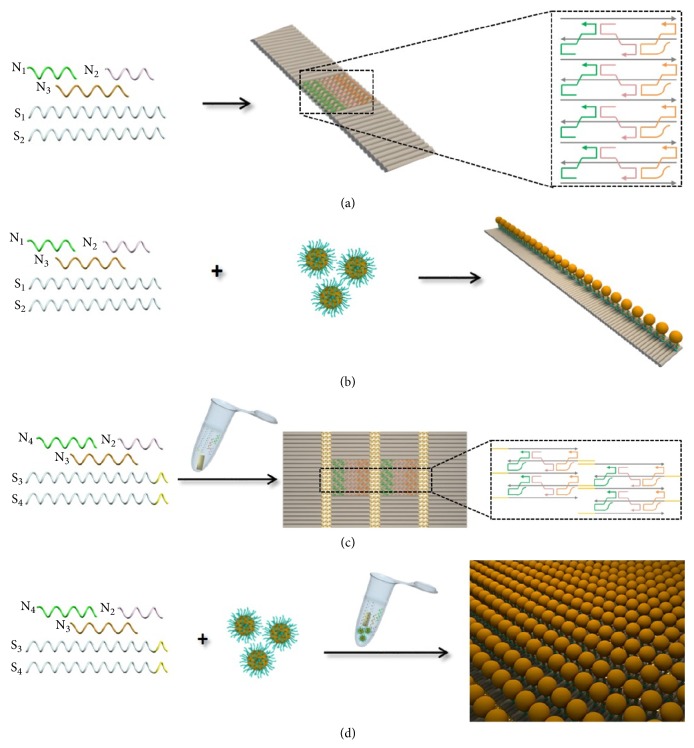
To assemble plasmonic gold metamaterials, ribbon-like DNA origami nanostructures (RDNs) were used as templates, in which three shorter DNA strands (N1, N2, and N3) not only fold two longer DNA strands (S1 and S2) into repeated rectangular units but connect neighbor units into long ribbons (Figure 1(a)). By extending N3 with a capture sequence as a binding site, AuNPs functionalized with thiol-DNA (SH-DNA-AuNPs) are mixed together with five strands in one pot to generate one-dimensional (1D) AuNPs lines. This strategy is also applied to organize gold nanorods (AuNRs) which functionalized with thiol-DNA (SH-DNA-AuNRs) into 1D AuNRs lines (Figure 1(b)). To obtain two-dimensional (2D) DNA lattices, S1 and S2 are extended with complementary overhangs of 15 bases into S3 and S4. Assisted by mica surface, five strands (N2, N3, N4, S3, and S4) are directly assembled into 2D lattices (Figure 1(c)). Using these lattices which have two binding sites on N3 and N4 as templates, 2D AuNPs lattices can be directly assembled with five strands in one pot assisted by mica (Figure 1(d)).
Figure 1.
Schematic illustration of the one-pot self-assembly of DNA nanostructures and plasmonic metamaterials. (a) RDNs. (b) AuNPs lines. (c) 2D DNA lattices assisted by mica. (d) AuNPs lattices assisted by mica.
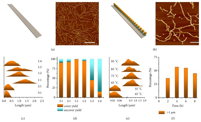
With the optimization of sequences for N1, N2, N3, S1, and S2 by SEQUIN [37], we surprisingly found that five DNA strands can self-assemble into RDNs in 20 minutes at room temperature in 1×TAE/Mg2+ buffer. AFM measurements showed that the lengths of RDNs were ranging from hundreds of nanometers to several micrometers and the width of RDNs was ~17 nm, which is in agreement with its theoretical value (Figures 2(a) and ). Using one-pot assembly strategy, we generated AuNPs lines with a high coverage rate up to 95% by simply mixing 5 nm-sized SH-DNA-AuNPs with five DNA strands (Figures 2(b) and ). To better understand the assembly process, we employed the two-step protocol to generate the AuNPs lines; that is, the RDNs templates were firstly assembled followed by anchoring of SH-DNA-AuNPs onto template surfaces. The coverage rate of thus assembled AuNPs lines was 45% (), which is significantly lower than the one obtained with the one-pot assembly strategy. In the one-pot assembly process, SH-DNA-AuNPs might hybridize with strand N3 that followed by folding with other strands into lines. While in the two-step assembly, the negative charged DNA nanoribbon may hinder the hybridization of SH-DNA-AuNPs to N3. In theory, the gap between neighboring N3 on the template is ~ 6 nm, which is big enough to anchor 5 nm-sized AuNPs.
Figure 2.
(a, b) Schematic illustrations and AFM images of 1D RDNs and 5 nm-sized AuNPs lines, scale bars: 500 nm. (c, d) Length density plots and coverage rate histogram of 5 nm-sized AuNPs lines on different ratios of AuNPs to stand N3. (e) Density plots of 5 nm-sized AuNPs lines on different initial temperature in annealing process. (f) Histogram of the percentage of micrometer-long AuNPs lines in different annealing time.
Different experimental conditions were systematically investigated. Micrometer-long AuNPs lines could be assembled with 99% coverage rate (Figures 2(c), 2(d), and ), with the optimized 1:1 concentration ratio of SH-DNA-AuNPs to N3. Considering that the RDNs can be easily assembled at room temperature, different initial temperatures for one-pot assembly were studied. When the initial temperature was equal to or higher than 65°C, micrometer-long AuNPs lines could be formed (Figures 2(e) and ). We also monitored the annealing time for one-pot assembly when the initial temperature was 65°C. After 2 h annealing, the percentage of micrometer-long AuNPs lines in the product was 36%, which was increased to 57% as prolonging the annealing time to 4 h (Figures 2(f) and ). We also examined the thermal stability of the 5 nm-sized AuNPs lines by keeping the samples in water bath with different temperature for 20 min. The AFM imaging results indicated that the structures were stable when they were heated to 40°C ().
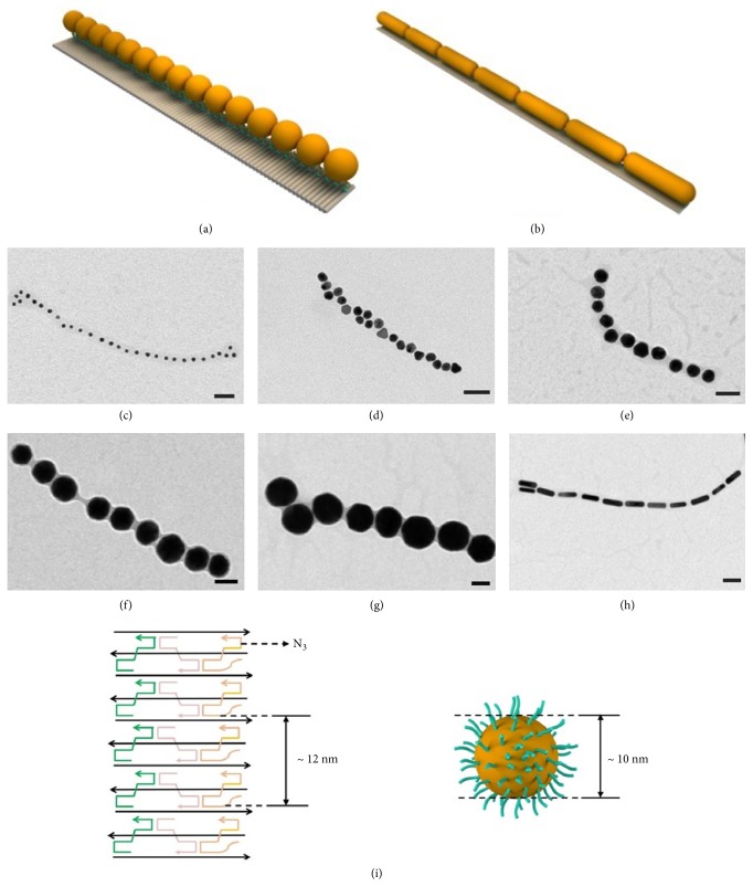
We further applied the one-pot assembly strategy to organize AuNPs of different sizes (Figure 3). TEM images validated the one-pot assembly of 10 nm-, 20 nm-, 30 nm-, 50 nm-, and 80 nm-sized AuNPs lines (Figures 3(c)–3(g) and ), which were obtained by annealing five strands with SH-DNA-AuNPs in 1×TAE/Mg2+ buffer from 65°C to 25°C in 4 h. To obtain high-quality 1D AuNPs lines, the concentration ratio of SH-DNA-AuNPs to N3 was optimized for AuNPs of different sizes. For example, 4 strands of N3 with other DNA strands form an 18 nm-long unit of nanoribbon, which are adapted to the size of 20 nm-sized AuNPs (Figure 3(i)), and the concentration ratio of 20 nm-sized AuNPs to N3 was 1:4. Correspondingly, the concentration ratio of SH-DNA-AuNPs to N3 was 1:2 and 1:6 for 10 nm- and 30 nm-sized AuNPs, 1:10 and 1:16 for 50 nm- and 80 nm-sized AuNPs, respectively.
Figure 3.
Schematic illustrations (a) and TEM images of 10 nm- (c), 20 nm- (d), 30 nm- (e), 50 nm- (f), and 80 nm-sized (g) AuNPs lines. Schematic illustrations (b) and TEM images of 20×70 nm-sized AuNRs lines (h). Scale bars: 50 nm. Four strands of N3 with other DNA strands form an 18 nm-long unit of nanoribbon which are adapted to the size of 20 nm-sized AuNPs (i).
With the increase of the size of AuNPs, the length of the AuNPs lines decreased from micrometers to hundreds of nanometers. These phenomena were adapted to the supposition we mentioned above; that is, SH-DNA-AuNPs may firstly hybridize with N3; therefore, it is more difficult for SH-DNA-AuNPs-N3 of larger sizes to further hybridize with other strands to form lines. Using the same one-pot assembly strategy, AuNRs (20×70 nm) were organized to form AuNRs lines with the concentration ratio of SH-DNA-AuNRs to N3 of 1:14, confirmed by TEM imaging results (Figures 3(h) and ).
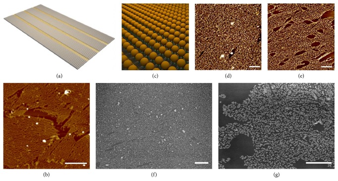
To widen the range of one-pot assembly strategy, we extended S1 and S2 with complementary 15-base overhangs. Five strands (N2, N3, N4, S3, and S4) were mixed together in 1×TAE/Mg2+ buffer and annealed from 65°C to 25°C for 12 h. Although there were some connections between RDNs, network-like DNA nanostructures other than 2D lattices were formed, demonstrated by AFM imaging results (). When mica was annealed together with five strands, the Mg2+ in buffer helped DNA strands to absorb onto mica surface and 2D DNA lattices were generated, which is validated by AFM images (Figures 4(a) and 4(b)). The growth processes of 2D lattices were proposed to be assisted by mica; that is, earlier formed RDNs could adsorb on negatively charged mica surface as nuclei and then single strands or smaller RDNs diffuse onto the surface for 2D crystallization. Using the one-pot assembly strategy, SH-DNA-AuNPs could be assembled into 2D AuNPs lattices assisted by mica (Figure 4(c)). AFM and SEM images demonstrated the formation of different-sized AuNPs 2D lattices (Figures 4(d)–4(g), , and ).
Figure 4.
Schematic illustrations (a) and AFM image (b) of 2D DNA lattices. Schematic illustrations (c) and AFM image of 5 nm- (d) and 10 nm-sized (e) AuNPs lattices, scale bars: 500 nm. SEM images of 20 nm-sized (f) and 30 nm-sized (g) AuNPs lattices, scale bars: 1 μm.
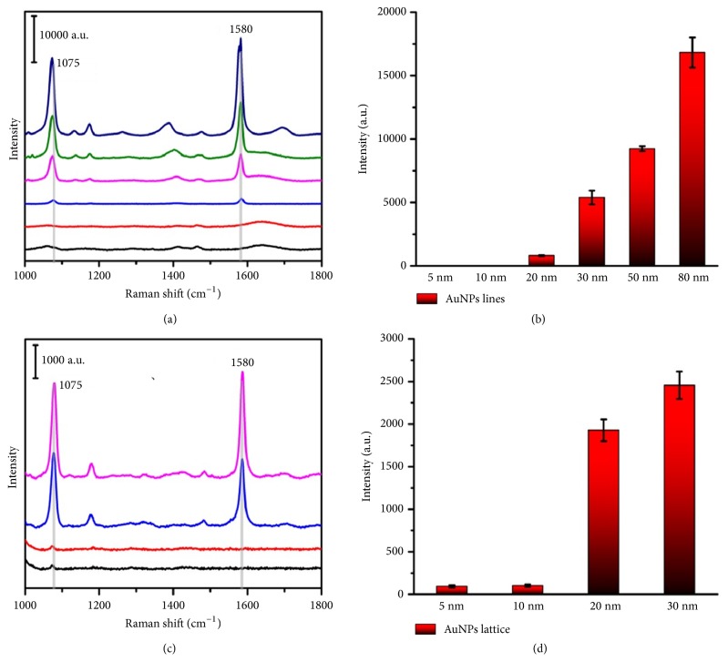
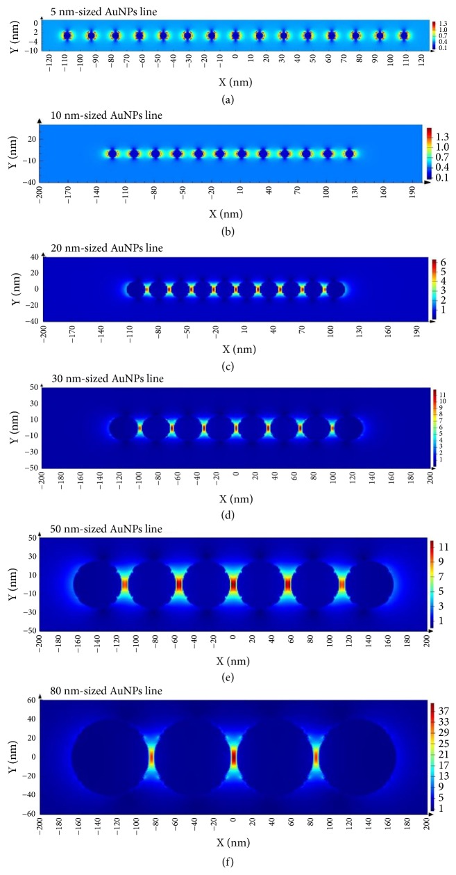
Because metal nanostructures can excite collectively coupled plasmons when in interacting with light, [15, 16] AuNPs metamaterials impelled us to consider their potential plasmonic properties [27, 38]. Previous studies showed that proper distances between individual AuNP could generate hot spots that induce stronger SERS signals. As most of the distances between the AuNPs in our 1D AuNPs lines and 2D AuNPs lattices were less than 10 nm, their coupling of the plasmons was detected by UV-vis absorption (). We used 4-MBA as a Raman-active molecule which could covalently attach to AuNPs via Au-S bond. The frequencies of 1580 cm−1 and 1075 cm−1 in the SERS spectra were attributed to 4-MBA. SERS signals were hardly observed from 5 nm- and 10 nm-sized AuNPs lines or lattices, because of the weak coupling of the larger gaps between small-sized AuNPs. However, large-sized AuNPs lines and lattices both induced enhanced SERS signals. Take the peak at 1075 cm−1 for an example; an enhanced signal generated by 80 nm-sized AuNPs lattices was twenty times higher than that of 20 nm-sized AuNPs lines (16833.93 to 804.98 a.u. at 1075 cm−1, Figure 5). Based on Maxwell's curl equations, the electrical field in different-sized AuNPs line upon illumination (Figure 6) was simulated by the comprehensive finite difference time domain (FDTD) method. On this basis, the enhancement could be naturally interpreted by the increasing of the hotspots created in the different-sized AuNPs lines. The same enhanced phenomenon was observed when comparing 20 nm- and 10 nm-sized AuNPs lattices.
Figure 5.
Typical SERS spectra of 1D AuNPs lines and 2D AuNPs lattices. (a) 5 nm- (black), 10 nm- (red), 20 nm- (blue), 30 nm- (purple), 50 nm- (green), and 80 nm-sized AuNPs lines (dark blue) with 4-MBA as the SERS reporter molecule. (b) Changes of the characteristic SERS intensity at 1075 cm−1 of different-sized AuNPs lines. (c) 5 nm- (black), 10 nm- (red), 20 nm- (blue), and 30 nm-AuNPs lattices (purple) with 4-MBA as the SERS reporter molecule. (d) Changes of the characteristic SERS intensity at 1075 cm−1 of different-sized AuNPs lattices.
Figure 6.
Finite-difference time-domain (FDTD) simulation of the electromagnetic field distributions of the different-sized AuNPs line. The gap between AuNPs is 10.6 nm (a), 12.7 nm (b), 2.7 nm (c), 2.8 nm (d), 5.9 nm (e), and 5.5 nm (f), respectively. The incident light is along x axis direction.
3. Discussion
We designed five-strand DNA tiles for the fabrication of DNA nanostructures in micrometer scale, which facilitate the realization of 1D and 2D plasmonic gold metamaterials. Using one-pot assembly strategy, AuNPs of different sizes are organized for high-quality 1D lines and 2D lattices, which could generate enhanced Raman scattering. This strategy is of great importance for single-step, rapid, and high-yield assembly of AuNPs into plasmonic metamaterials. As semiconductor and information technologies approach their physical limits, it is a great challenge to combine the functionality of biological systems and semiconductors. Our strategy would provide a potential tool to deal with interfacing biological materials with conventional semiconductors for practical applications.
4. Materials and Methods
4.1. Preparation of SH-DNA-AuNPs/AuNRs Conjugates
5 μL of 100 μM SH-DNA and 100 μL of 83.3 nM 5 nm-sized spherical AuNPs were mixed together in 0.5 × TBE buffer (89 mM Tris, 89 mM boric acid, 2 mM EDTA, pH 8.0), which was incubated at 37°C for about 4 h. 10 μL 3 M NaCl was gradually added to reach a final concentration of 0.3 M NaCl for aging. The solution was kept in 37°C overnight. To remove excess SH-DNA, the solution was centrifuged (12000 rpm, 25 min) and the supernatant was carefully removed by pipette. The SH-DNA-AuNPs conjugates were washed by 0.5 × TBE buffer for three times. For spherical AuNPs of different diameters, the protocols were identical except that the ratios of 10 nm-, 20 nm-, 30 nm-, 50 nm-, and 80 nm-sized AuNPs to DNA were approximately 1:300. For 20 × 70 nm gold nanorods (AuNRs), excess amounts of cetyltrime-thyl ammonium bromide in the AuNRs solution had to be removed by centrifugation at 4000 rpm for 10 min and the ratio of AuNPs to DNA was approximately 1:600.
4.2. One-Pot Assembly of RDNs, AuNPs, and AuNRs Lines
Stock solutions (5 μM) of DNA single strand (N1, N2, N3, S1, and S2) were mixed together (2 μL for each strand) in 20 minutes at room temperature. The RDNs were obtained with a final concentration of 500 nM in TAE buffer (40 × 10−3 M Tris, 20 × 10−3 M acetic acid, 2 × 10⁻³ M EDTA, and 12.5 × 10⁻³ M magnesium acetate, pH 8.0). For 5 nm-sized AuNPs lines, 5 μM ssDNA stock solutions (N1, N2, N3, S1, and S2, 2 μL for each) and SH-DNA-AuNPs (the ratio of SH-DNA-AuNPs to strand N3 was 1:1) were mixed together and annealed from 65°C to 25°C for 4 h. The protocols for AuNPs lines of different diameters were identical except that the ratios of 10 nm-, 20 nm-, 30 nm-, 50 nm-, and 80 nm-sized AuNPs to N3 were 1:2, 1:4, 1:6, 1:10, and 1:16. For the AuNRs lines, the ratio of 20 × 70 nm AuNRs to N3 was 1:14.
4.3. One-Pot Assembly of Two-Dimensional (2D) DNA and AuNPs Lattices
5 μM ssDNA stock solutions (N2, N3, N4, S3, and S4, 2 μL for each) were mixed together with mica in TAE buffer. The mixture was annealed in 2L water from 65°C to 25°C for 12 h to assemble 2D DNA lattices. For 5 nm-sized AuNPs lattices, 5 μM ssDNA stock solutions (N2, N3, N4, S3, and S4, 2 μL for each) and SH-DNA-AuNPs (the ratio of SH-DNA-AuNPs to N3 was 1:1) were mixed together with mica in TAE buffer and annealed from 65°C to 25°C for 12 h. The protocols for AuNPs lattices of different sizes were identical.
4.4. AFM Characterization
5 μL of RDNs or AuNPs lines was deposited onto the fresh cleaved mica, allowing for 3-5min adsorption. The samples were rinsed with pure water, dried under nitrogen, and then scanned in tapping mode by MultiMode 8 AFM with NanoScope V Controller (Bruker, Inc.).
4.5. TEM Characterization
For TEM imaging, 10 μL of the sample was dropped on a carbon-coated grid (400 mesh; Ted Pella, Inc.). After 15 min deposition, the excess amounts of solution drop on the grid were wicked by a drop of water and then adsorbed into a filter paper. TEM images were obtained by a Tecnai G2-20S TWIN system, which was operated at 100 kV in a bright-field mode.
4.6. SEM Characterization
2D AuNPs lattices on the mica were washed by pure water and dried under nitrogen. The samples were rinsed with positively charged nanogold solution for 15 s to increase the conductivity. Then the mica was stuck to the sample table by conductive tape. SEM imaging was performed using a HITACHI S4800 at 80 kV in dark field mode.
4.7. SERS Characterization
Samples of AuNPs lines were incubated in 1 mM 4-MBA ethanolic solution for 2-3 h. 25 mL of the sample was deposited on a silicon substrate and performed in solution for SERS characterization. 10 μL 10 mM 4-MBA ethanolic solution was deposited onto the mica surfaces with 2D AuNPs lattices for over 3 h, followed by a thorough rinse with pure ethanol. The SERS characterization was performed on mica surface. For all measurements, the confocal Raman microscope (Invia, Renishaw, England) was employed with a 633 nm He-Ne laser at the power of 0.08 mW. Other experimental parameters were as follows: objective 20×, acquisition time 10 s, slit of 100 μm, resolution grating of 1800 grooves, and spectra ranged from 1000 to 1800 cm −1.
Acknowledgments
This work was supported by the Ministry of Science and Technology of China (2017YFA0205302), the NSFC (61771253, 61671250, and 61871236), the Program for Changjiang Scholars and Innovative Research Team in University (IRT 15R37), and the Priority Academic Program Development of Jiangsu Higher Education Institutions (PAPD, YX03001).
Contributor Information
Jie Chao, Email: iamjchao@njupt.edu.cn.
Lianhui Wang, Email: iamlhwang@njupt.edu.cn.
Chunhai Fan, Email: fanchunhai@sjtu.edu.cn.
Data Availability
All data is available in the main text or the Supplementary Materials.
Conflicts of Interest
The authors declare no conflicts of interest.
Authors' Contributions
Jie Chao, Lianhui Wang, and Chunhai Fan conceived the idea and designed the experiment. Jun Wang, Shaokang Ren, Nan Teng, Dan Zhu, and Shao Su conducted the experiment and performed the AFM, TEM, and SEM measurements. Chunyuan Song, Yanjun Yang, and Qian Li performed the Raman measurements. All authors contributed equally to the writing of the manuscript. Shaokang Ren and Jun Wang contributed equally to this work.
Supplementary Materials
Supplementary Figure 1: schematic illustrations and AFM images of 1D RDNs. (a) The design of RDNs is that two 48nt sequences are folded by three staple strands into a ribbon like DNA nanostructure. (b) AFM image of RDNs. Scale bar: 500 nm. (c) AFM height and width images with corresponding line scans (inset of (b)) for bare RDNs. (d) Histogram of RDNs length counts. Supplementary Figure 2: 1D AuNPs lines. Schematics (a, b) and AFM images (c, d) are single- and two-step assembly of 5 nm-sized AuNPs lines, respectively. Scale bars: 500 nm. (e) Coverage rate histogram of single- and two-step assembly of AuNPs lines. Supplementary Figure 3: analysis and AFM images of 5 nm-sized AuNPs lines at different annealing temperatures. (a) 45°C. (b) 55°C. (c) 65°C. (d) 75°C. (e) 85°C. (f) 95°C. Scale bars: 200 nm. Supplementary Figure 4: analysis and AFM images of 5 nm-sized AuNPs lines at different ratio of AuNPs to RDNs when annealing temperature is 65°C. (a) 3:1. (b) 2:1. (c) 1:1. (d) 1:2. (e) 1:3. (f) 1:4. Scale bars: 200 nm. Supplementary Figure 5: annealing temperature is 65°C and the ratio of AuNPs to RDNs is 1:1; analysis and AFM images of 5 nm-sized AuNPs lines with annealing time. (a) 0.1 h. (b) 0.5 h. (c) 1 h. (d) 1.5 h. (e) 2 h. (f) 4 h. (g) 6 h. (h) 8 h. Scale bars: 200 nm. Supplementary Figure 6: AFM images of 5 nm-sized AuNP lines which were heated to 30°C, 40°C, 50°C, and 60°C. Scale bars: 200 nm. Supplementary Figure 7: schematic illustrations and more TEM images of organized different sizes of AuNPs lines. (a) 10 nm-sized AuNPs lines. (b) 20 nm-sized AuNPs lines. (c) 30 nm-sized AuNPs lines. (d) 50 nm-sized AuNPs lines. (e) 80 nm-sized AuNPs lines. (f) 20×70 nm-sized AuNRs lines. Scale bars: 50 nm. Supplementary Figure 8: AFM images of 2D DNA lattices without mica surface-mediated and height and width image with corresponding line scans (inset of (c)) for 2D DNA lattices. Supplementary Figure 9: AFM images of 2D DNA lattices (a) and 2D AuNPs lattices of mica surface-mediated. (b) 5 nm-sized AuNPs lattices. (c) 10 nm-sized AuNPs lattices. SEM images of 20 nm-sized (d) and 30 nm-sized (e) AuNPs lattices. Supplementary Figure 10: AFM images of 5 nm-sized SH-DNA-AuNPs (a) and 2D DNA lattices (b) and 5 nm-sized AuNPs lattices. Scale bar: 50 nm. Supplementary Figure 11: UV–Vis characterization of different-sized AuNPs lines.
References
- 1.Teschome B., Facsko S., Gothelf K. V., Keller A. Alignment of gold nanoparticle-decorated dna origami nanotubes: substrate prepatterning versus molecular combing. Langmuir. 2015;31(46):12823–12829. doi: 10.1021/acs.langmuir.5b02569. [DOI] [PubMed] [Google Scholar]
- 2.Gür F. N., Schwarz F. W., Ye J., Diez S., Schmidt T. L. Toward self-assembled plasmonic devices: high-yield arrangement of gold nanoparticles on DNA origami templates. ACS Nano. 2016;10(5):5374–5382. doi: 10.1021/acsnano.6b01537. [DOI] [PubMed] [Google Scholar]
- 3.Bayrak T., Helmi S., Ye J., et al. DNA-mold templated assembly of conductive gold nanowires. Nano Letters. 2018;18(3):2116–2123. doi: 10.1021/acs.nanolett.8b00344. [DOI] [PubMed] [Google Scholar]
- 4.Gür F. N., McPolin C. P., Raza S., et al. DNA-assembled plasmonic waveguides for nanoscale light propagation to a fluorescent nanodiamond. Nano Letters. 2018;18(11):7323–7329. doi: 10.1021/acs.nanolett.8b03524. [DOI] [PubMed] [Google Scholar]
- 5.Sharma J., Chhabra R., Liu Y., Ke Y., Yan H. DNA-templated self-assembly of two-dimensional and periodical gold nanoparticle arrays. Angewandte Chemie International Edition. 2006;45(5):730–735. doi: 10.1002/anie.200503208. [DOI] [PubMed] [Google Scholar]
- 6.Sharma J., Chhabra R., Cheng A., Brownell J., Liu Y., Yan H. Control of self-assembly of DNA tubules through integration of gold nanoparticles. Science. 2009;323(5910):112–116. doi: 10.1126/science.1165831. [DOI] [PMC free article] [PubMed] [Google Scholar]
- 7.Yao G., Li J., Chao J., et al. Gold-nanoparticle-mediated jigsaw-puzzle-like assembly of supersized plasmonic DNA origami. Angewandte Chemie International Edition. 2015;54(10):2966–2969. doi: 10.1002/anie.201410895. [DOI] [PubMed] [Google Scholar]
- 8.Liu W., Halverson J., Tian Y., Tkachenko A. V., Gang O. Self-organized architectures from assorted DNA-framed nanoparticles. Nature Chemistry. 2016;8(9):867–873. doi: 10.1038/nchem.2540. [DOI] [PubMed] [Google Scholar]
- 9.Schreiber R., Santiago I., Ardavan A., Turberfield A. J. Ordering gold nanoparticles with DNA origami nanoflowers. ACS Nano. 2016;10(8):7303–7306. doi: 10.1021/acsnano.6b03076. [DOI] [PubMed] [Google Scholar]
- 10.Wang P., Gaitanaros S., Lee S., Bathe M., Shih W. M., Ke Y. Programming self-assembly of DNA origami honeycomb two-dimensional lattices and plasmonic metamaterials. Journal of the American Chemical Society. 2016;138(24):7733–7740. doi: 10.1021/jacs.6b03966. [DOI] [PubMed] [Google Scholar]
- 11.Lin C., Liu Y., Yan H. Designer DNA nanoarchitectures. Biochemistry. 2009;48(8):1663–1674. doi: 10.1021/bi802324w. [DOI] [PMC free article] [PubMed] [Google Scholar]
- 12.Tian Y., Zhang Y., Wang T., et al. Lattice engineering via nanoparticle-DNA frameworks. Nature Materials. 2016;15(6):654–661. doi: 10.1038/nmat4571. [DOI] [PMC free article] [PubMed] [Google Scholar]
- 13.Xu X., Rosi N. L., Wang Y., Huo F., Mirkin C. A. Asymmetric functionalization of gold nanoparticles with oligonucleotides. Journal of the American Chemical Society. 2006;128(29):9286–9287. doi: 10.1021/ja061980b. [DOI] [PMC free article] [PubMed] [Google Scholar]
- 14.Chao J., Lin Y., Liu H., Wang L., Fan C. DNA-based plasmonic nanostructures. Materials Today. 2015;18(6):326–335. doi: 10.1016/j.mattod.2015.01.018. [DOI] [Google Scholar]
- 15.Lee A., Andrade G. F., Ahmed A., et al. Probing dynamic generation of hot-spots in self-assembled chains of gold nanorods by surface-enhanced raman scattering. Journal of the American Chemical Society. 2011;133(19):7563–7570. doi: 10.1021/ja2015179. [DOI] [PubMed] [Google Scholar]
- 16.Thacker V. V., Herrmann L. O., Sigle D. O., et al. DNA origami based assembly of gold nanoparticle dimers for surface-enhanced Raman scattering. Nature Communications. 2014;5(1):p. 3448. doi: 10.1038/ncomms4448. [DOI] [PubMed] [Google Scholar]
- 17.Wu X., Xu L., Liu L., et al. Unexpected chirality of nanoparticle dimers and ultrasensitive chiroplasmonic bioanalysis. Journal of the American Chemical Society. 2013;135(49):18629–18636. doi: 10.1021/ja4095445. [DOI] [PubMed] [Google Scholar]
- 18.McPeak K. M., van Engers C. D., Bianchi S., et al. Ultraviolet plasmonic chirality from colloidal aluminum nanoparticles exhibiting charge-selective protein detection. Advanced Materials. 2015;27(40):6244–6250. doi: 10.1002/adma.201503493. [DOI] [PubMed] [Google Scholar]
- 19.Deng Z., Mao C. Molecular lithography with DNA nanostructures. Angewandte Chemie International Edition. 2004;43(31):4068–4070. doi: 10.1002/anie.200460257. [DOI] [PubMed] [Google Scholar]
- 20.Hung A. M., Micheel C. M., Bozano L. D., et al. Large-area Spatially ordered arrays of gold nanoparticles directed by lithographically confined DNA origami. Nature Nanotechnology. 2010;5(2):121–126. doi: 10.1038/nnano.2009.450. [DOI] [PubMed] [Google Scholar]
- 21.Mirkin C. A., Letsinger R. L., Mucic R. C., Storhoff J. J. A DNA-based method for rationally assembling nanoparticles into macroscopic materials. Nature. 1996;382(6592):607–609. doi: 10.1038/382607a0. [DOI] [PubMed] [Google Scholar]
- 22.Alivisatos A. P., Johnsson K. P., Peng X., et al. Organization of ‘nanocrystal molecules’ using DNA. Nature. 1996;382(6592):609–611. doi: 10.1038/382609a0. [DOI] [PubMed] [Google Scholar]
- 23.Seeman N. C. DNA in a material world. Nature. 2003;421(6921):427–431. doi: 10.1038/nature01406. [DOI] [PubMed] [Google Scholar]
- 24.Ma Y., Zheng H., Wang C., et al. RCA strands as scaffolds to create nanoscale shapes by a few staple strands. Journal of the American Chemical Society. 2013;135(8):2959–2962. doi: 10.1021/ja400102s. [DOI] [PubMed] [Google Scholar]
- 25.Seeman N. C., Fan C., Wang S., et al. Forum on Translational DNA Nanotechnology. ACS Applied Materials & Interfaces. 2019;11(15):13833–13834. doi: 10.1021/acsami.9b04482. [DOI] [PubMed] [Google Scholar]
- 26.Rothemund P. W. K. Folding DNA to create nanoscale shapes and patterns. Nature. 2006;440(7082):297–302. doi: 10.1038/nature04586. [DOI] [PubMed] [Google Scholar]
- 27.Zhao M., Wang X., Xing Y., et al. DNA origami-templated assembly of plasmonic nanostructures with enhanced raman scattering. Nuclear Science and Techniques. 2017;29(1) [Google Scholar]
- 28.Liu X., Zhang F., Jing X., et al. Complex silica composite nanomaterials templated with DNA origami. Nature. 2018;559(7715):593–598. doi: 10.1038/s41586-018-0332-7. [DOI] [PubMed] [Google Scholar]
- 29.Lo P. K., Karam P., Aldaye F. A., et al. Loading and selective release of cargo in DNA nanotubes with longitudinal variation. Nature Chemistry. 2010;2(4):319–328. doi: 10.1038/nchem.575. [DOI] [PubMed] [Google Scholar]
- 30.Shen J., Tang Q., Li L., et al. Valence-engineering of quantum dots using programmable DNA scaffolds. Angewandte Chemie. 2017;129(50):16293–16297. doi: 10.1002/ange.201710309. [DOI] [PubMed] [Google Scholar]
- 31.Liu Q., Ge Z., Mao X., et al. Valency-controlled framework nucleic acid signal amplifiers. Angewandte Chemie-international Edition. 2018;57(24):7131–7135. doi: 10.1002/anie.201802701. [DOI] [PubMed] [Google Scholar]
- 32.Zhao Z., Liu Y., Yan H. Organizing DNA origami tiles into larger structures using preformed scaffold frames. Nano Letters. 2011;11(7):2997–3002. doi: 10.1021/nl201603a. [DOI] [PMC free article] [PubMed] [Google Scholar]
- 33.Hamada S., Murata S. Substrate-assisted assembly of interconnected single-duplex DNA nanostructures. Angewandte Chemie International Edition. 2009;48(37):6820–6823. doi: 10.1002/anie.200902662. [DOI] [PubMed] [Google Scholar]
- 34.Kim J., Ha T. H., Park S. H. Substrate-assisted 2D DNA lattices and algorithmic lattices from single-stranded tiles. Nanoscale. 2015;7(29):12336–12342. doi: 10.1039/C5NR03088A. [DOI] [PubMed] [Google Scholar]
- 35.Aghebat Rafat A., Pirzer T., Scheible M. B., Kostina A., Simmel F. C. Surface-assisted large-scale ordering of DNA origami tiles. Angewandte Chemie International Edition. 2014;53(29):7665–7668. doi: 10.1002/anie.201403965. [DOI] [PubMed] [Google Scholar]
- 36.Woo S., Rothemund P. W. Self-assembly of Two-dimensional DNA origami lattices using cation-controlled surface diffusion. Nature Communications. 2014;5:p. 4889. doi: 10.1038/ncomms5889. [DOI] [PubMed] [Google Scholar]
- 37.Seeman N. C. De Novo design of sequences for nucleic acid structural engineering. Journal of Biomolecular Structure and Dynamics. 1990;8(3):573–581. doi: 10.1080/07391102.1990.10507829. [DOI] [PubMed] [Google Scholar]
- 38.Liu B., Song C., Zhu D., et al. DNA-origami-based assembly of anisotropic plasmonic gold nanostructures. Small. 2017;13(23):1–8. doi: 10.1002/smll.201603991. [DOI] [PubMed] [Google Scholar]
Associated Data
This section collects any data citations, data availability statements, or supplementary materials included in this article.
Supplementary Materials
Supplementary Figure 1: schematic illustrations and AFM images of 1D RDNs. (a) The design of RDNs is that two 48nt sequences are folded by three staple strands into a ribbon like DNA nanostructure. (b) AFM image of RDNs. Scale bar: 500 nm. (c) AFM height and width images with corresponding line scans (inset of (b)) for bare RDNs. (d) Histogram of RDNs length counts. Supplementary Figure 2: 1D AuNPs lines. Schematics (a, b) and AFM images (c, d) are single- and two-step assembly of 5 nm-sized AuNPs lines, respectively. Scale bars: 500 nm. (e) Coverage rate histogram of single- and two-step assembly of AuNPs lines. Supplementary Figure 3: analysis and AFM images of 5 nm-sized AuNPs lines at different annealing temperatures. (a) 45°C. (b) 55°C. (c) 65°C. (d) 75°C. (e) 85°C. (f) 95°C. Scale bars: 200 nm. Supplementary Figure 4: analysis and AFM images of 5 nm-sized AuNPs lines at different ratio of AuNPs to RDNs when annealing temperature is 65°C. (a) 3:1. (b) 2:1. (c) 1:1. (d) 1:2. (e) 1:3. (f) 1:4. Scale bars: 200 nm. Supplementary Figure 5: annealing temperature is 65°C and the ratio of AuNPs to RDNs is 1:1; analysis and AFM images of 5 nm-sized AuNPs lines with annealing time. (a) 0.1 h. (b) 0.5 h. (c) 1 h. (d) 1.5 h. (e) 2 h. (f) 4 h. (g) 6 h. (h) 8 h. Scale bars: 200 nm. Supplementary Figure 6: AFM images of 5 nm-sized AuNP lines which were heated to 30°C, 40°C, 50°C, and 60°C. Scale bars: 200 nm. Supplementary Figure 7: schematic illustrations and more TEM images of organized different sizes of AuNPs lines. (a) 10 nm-sized AuNPs lines. (b) 20 nm-sized AuNPs lines. (c) 30 nm-sized AuNPs lines. (d) 50 nm-sized AuNPs lines. (e) 80 nm-sized AuNPs lines. (f) 20×70 nm-sized AuNRs lines. Scale bars: 50 nm. Supplementary Figure 8: AFM images of 2D DNA lattices without mica surface-mediated and height and width image with corresponding line scans (inset of (c)) for 2D DNA lattices. Supplementary Figure 9: AFM images of 2D DNA lattices (a) and 2D AuNPs lattices of mica surface-mediated. (b) 5 nm-sized AuNPs lattices. (c) 10 nm-sized AuNPs lattices. SEM images of 20 nm-sized (d) and 30 nm-sized (e) AuNPs lattices. Supplementary Figure 10: AFM images of 5 nm-sized SH-DNA-AuNPs (a) and 2D DNA lattices (b) and 5 nm-sized AuNPs lattices. Scale bar: 50 nm. Supplementary Figure 11: UV–Vis characterization of different-sized AuNPs lines.
Data Availability Statement
All data is available in the main text or the Supplementary Materials.


