Abstract
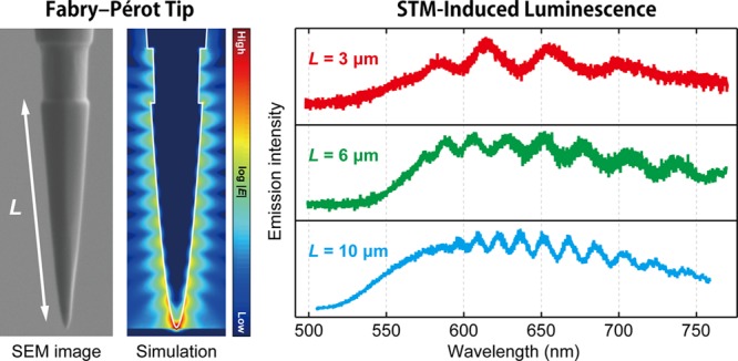
Near-field manipulation in plasmonic nanocavities can provide various applications in nanoscale science and technology. In particular, a gap plasmon in a scanning tunneling microscope (STM) junction is of key interest to nanoscale imaging and spectroscopy. Here we show that spectral features of a plasmonic STM junction can be manipulated by nanofabrication of Au tips using focused ion beam. An exemplary Fabry–Pérot type resonator of surface plasmons is demonstrated by producing the tip with a single groove on its shaft. Scanning tunneling luminescence spectra of the Fabry–Pérot tips exhibit spectral modulation resulting from interference between localized and propagating surface plasmon modes. In addition, the quality factor of the plasmonic Fabry–Pérot interference can be improved by optimizing the overall tip shape. Our approach paves the way for near-field imaging and spectroscopy with a high degree of accuracy.
Keywords: Nanooptics, plasmonic nanocavity, scanning tunneling luminescence
Manipulation of near-field properties, such as a spectral response, optical coupling to far fields, and local field enhancement, by using metallic nanostructures is a foundation of plasmonics, providing a wide range of applications in nanooptics,1 single-molecule sensing,2 and enhancement of photovoltaics,3 and photochemistry.4 Advances of nanoscale fabrication techniques have allowed one to control surface plasmons at metal–dielectric interfaces,5 leading to the discovery of exotic properties of near-field optics such as the extraordinary high transmission through subwavelength holes.6 Plasmon excitation in nanoscale cavities is of particular importance due to dramatic enhancement and extreme confinement of an electromagnetic field,7 which results in strong light–matter interactions.8
Plasmonic nanocavities formed by a sharp tip of a scanning probe microscope and a surface play a central role in nanoscale imaging and spectroscopy well below the diffraction limit and even down to the single-molecule level. Scanning near-field optical microscopy (SNOM) is today widely used to resolve surface morphologies with a typical spatial resolution of 10–20 nm.9,10 Furthermore, tip-enhanced Raman spectroscopy (TERS) has attracted increasing attention as powerful vibrational nanospectroscopy.11−14 In addition, scanning tunneling luminescence (STL) can be used to investigate localized surface plasmon resonance (LSPR) confined in nanoscale cavities15 and more recently has demonstrated highly accurate single-molecule spectroscopy.16−23 These studies open up new opportunities to elucidate fundamental aspects of near-field physics and chemistry with (sub)nanometer spatial resolution. From this perspective, active control of plasmonic properties in scanning tunneling microscope (STM) junctions is one important technical milestone but the correlation between the LSPR and the tip geometry has been examined only qualitatively.24−26 Here we report an attempt to manipulate LSPR in STM junctions by nanofabricating Au tips using focused ion beam (FIB) and demonstrate spectral modulation through a Fabry–Perot type interference of surface plasmons.
Figure 1a,b shows scanning electron microscope (SEM) images of an electrochemically etched Au tip before and after FIB fabrication (the latter is denoted as FIB-tip hereafter). A typical apex diameter of ∼20 nm is obtained (Figure 1c). The STL spectra recorded over the Ag(111) surface at 78 K (Figure 1d) show a single broad peak resulting from LSPR excitation in the junction which in good agreement with electrodynamic simulations.27 Although the FIB-tip may contain embedded Ga atoms, the STL intensity was not much different from standard tips prepared by electrochemical etching. Figure 1d also shows the bias voltage dependence of the STL spectra and the emission intensity becomes stronger at higher voltages. Quenching of light emission at short wavelengths arises from the quantum cutoff28 at low voltages and from the 5d → 6sp interband transition of Au at high voltages.29
Figure 1.
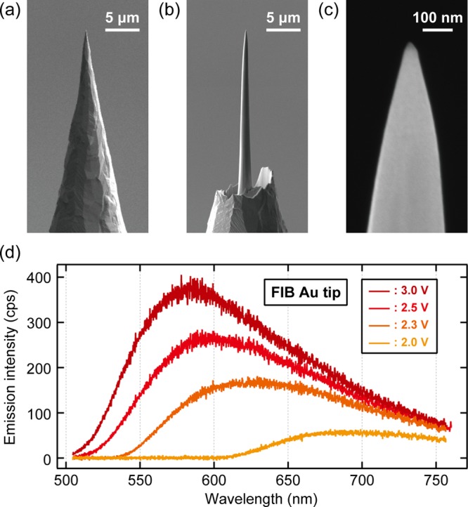
FIB fabrication of an Au tip and STL spectra. (a,b) SEM images of an Au tip before and after FIB milling. (c) Magnified SEM image of the tip apex of the FIB fabricated tip. (d) Bias voltage dependence of STL spectra measured over the Ag(111) surface with the FIB-tip (It = 9 nA, Vbias is indicated in the figure).
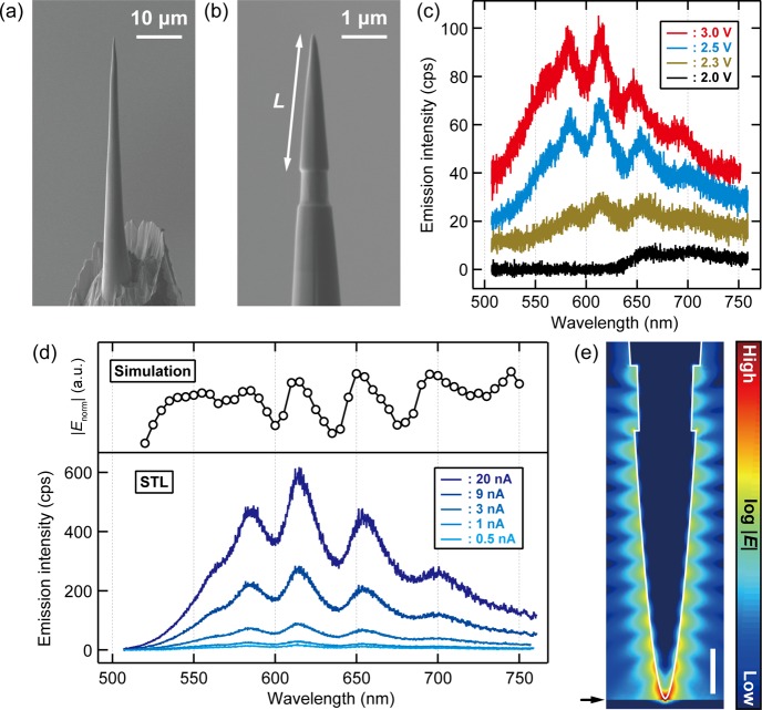
We found that the STL spectra can be modulated by plasmonic Febry–Pérot interference. Such an interference has been examined previously in several different plasmonic nanostructures such as nanowires30−33 and thin metal films with a slit/groove pair.34−36 The LSPR excitation in an STM junction occurs through inelastic electron tunneling,15 which also launches propagating surface plasmon polaritons (SPPs) on the tip shaft as well as on the sample surface.37 In order to reflect the propagating modes back to the apex, a single groove was fabricated on the smooth tip shaft at a distance L from the apex. In Figure 2b, the groove (725 nm long and 100 nm deep) is located at 3 μm away from the apex. Reflection of the SPPs at the groove results in standing wave formation on the tip shaft, which couples to the localized mode in the junction and causes spectral modulation in light emission from the junction. As shown later (Figure 4), light emission also occurs at the groove.
Figure 2.
STL spectra of a grooved tip. (a,b) SEM image of the FIB processed Au tip with a groove located 3 μm away from the tip apex. (c) Bias voltage dependence of STL spectra measured over the Ag(111) surface with the grooved tip (It = 1 nA, Vbias is indicated in the figure). (d) Tunneling current dependence of STL spectra measured over the Ag(111) surface with the grooved tip (Vbias = 2.5 V, It is indicated in the figure). The top panel shows the wavelength dependence of the numerically simulated electric field inside the junction 2 Å below the apex. (e) Normalized electric field distribution plotted on a logarithmic scale simulated for L = 3 μm and at 610 nm. The white lines indicate the tip shape and the black arrow indicates the position of the Ag surface. The scale bar is 500 nm.
Figure 4.
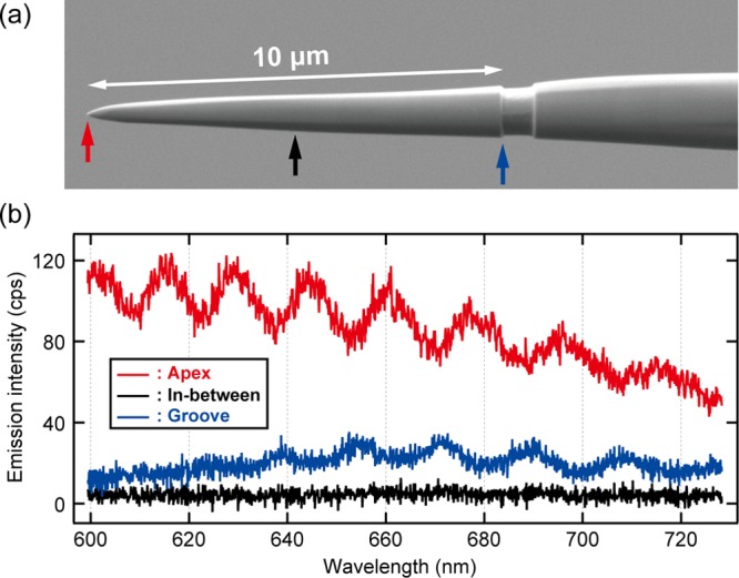
STL spectra recorded at different positions on the grooved tip. (a) SEM image of the grooved tip with L = 10 μm. (b) STML spectra obtained at the apex (red), the groove (blue), and in-between (black) (Vbias = 2.5 V, It = 9 nA).
Figure 2c shows the voltage-dependent STL spectra obtained with the grooved tip. The spectra exhibit a periodic oscillation caused by the Febry–Pérot type interference on the tip shaft. The emission intensity increases with increasing the bias voltage and the peak positions are slightly blue-shifted at long wavelengths (>650 nm, see Supporting Information). However, the peak positions are independent of the tunneling current (bottom panel of Figure 2d) and the STL intensity linearly depends on the current (see Supporting Information). The increase of the tunneling current also leads to a decrease of the tip–surface distance. A change in the current from 0.5 to 20 nA approximately corresponds to a relative displacement of 1–2 Å. The STL intensity (i.e., local field enhancement) is determined by the tip–surface distance and/or the amount of tunneling electrons that excite the LSPR in the junction via an inelastic tunneling process. The linear dependence of the STL intensity on the tunneling current suggests that the latter contribution is dominant.
To understand the plasmonic Fabry-Pérot interference observed for the grooved tip, we performed numerical simulations of the plasmonic response in the STM junction upon excitation by an oscillating point dipole located under the tip and oriented along the tip axis (see Supporting Information for details). The tip shape was taken from the SEM image (Figure 2b). Figure 2e displays the electric field distribution at 610 nm excitation simulated for a grooved tip with L = 3 μm, revealing the standing wave formation on the tip shaft. The simulated wavelength dependence of the electric field in the junction (see top panel of Figure 2d) shows that the peak positions coincide with experiment. This result corroborates that the spectral modulation of the grooved tip occurs through the plasmonic Fabry–Pérot interference. The formation of similar standing wave patterns on plasmonic nanotips (Au tapers) has been observed in real-space using electron energy loss spectroscopy (EELS).38−40 As discussed in previous studies,39,40 the taper structure can support not only the fundamental azimuthal mode (m = 0) but also higher-order modes (m ≥ 1). However, because only the radially symmetric m = 0 mode can be supported at the apex, this mode is expected to be excited predominantly by the STM excitation, whereas the m ≥ 1 modes exhibit a cutoff behavior at a distance from the apex.41,42
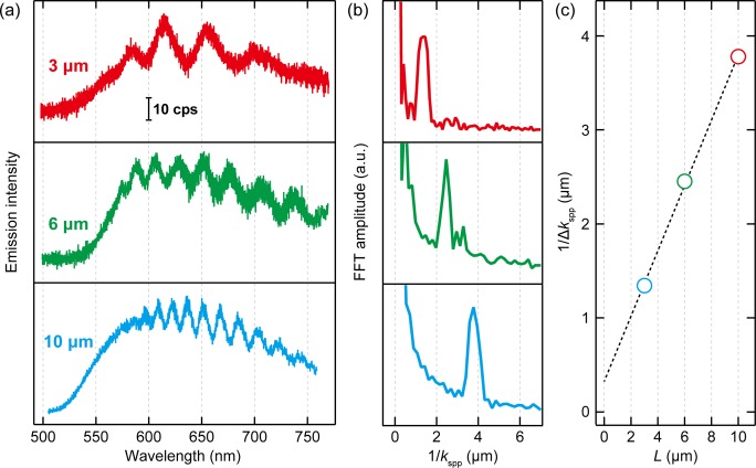
The plasmonic Fabry–Pérot resonance can be tuned by the groove position. Figure 3a shows the STL spectra obtained for tips with a groove at L = 3, 6, and 10 μm and the peak spacing decreases with distance. For the Au–vacuum interface, the propagation length of the SPP is estimated to be 30–80 μm in the wavelength range of 500–750 nm (by assuming a simple Drude model). Thus, the SPP can propagate between the apex and the groove along the tip shaft and may undergo several reflections (round trips). Figure 3b shows the Fourier spectra with the wave vector of the surface plasmon polariton (kspp) calculated by the Drude model for a planar Au–vacuum interface. The Fourier spectra exhibit a single peak but higher-order peaks are absent, indicating a significant decay (loss) of the SPPs due to damping into the metal as well as coupling to far-field radiation at the apex and the groove. Under such a low quality (Q) factor condition, the emission intensity (I) from the apex (or analogous from the groove) can be approximated by
| 1 |
where ELSP and ESPP correspond to the amplitude of the localized mode at the apex (or groove) and the propagating SPPs, whereas the third term accounts for their interference. Scattering of the SPPs to far-field radiation can be neglected on the shaft since coupling of the surface bound wave to free space does not occur in case of extremely low surface roughness43 as obtained from the FIB milling. The phase factor of the modulation due to the SPP reflection is given by
| 2 |
where kSPP is the SPP wave vector and ϕ0 accounts
for an additional (unknown) phase shift upon SPPs reflection at the
groove. Although we could not determine ϕ0, previous
studies estimated it to be on the order of π for Au thin films
with the double-slit or slit-groove pair structures.36,44 The SPP wave vector is given by kSPP = k0neff where k0 = 2π/λ is the free-space
wave vector (λ, wavelength) and neff is the effective refractive index which is, for a simple planar
metal–dielectric interface, given by  with the dielectric constant of the metal
(εm) and the surrounding dielectric (εd).
Figure 3.
STL spectra of grooved tips with different apex–groove distances. (a) STML spectra measured over the Ag(111) surface using Au tips with grooves located at L = 3, 6, and 10 μm (Vbias = 2.5 V, It = 9 nA). (b) Fourier spectra of (a) executed for the interpolated data with kspp. (c) The peak position (1/Δkspp) in (b) is plotted as a function of L.
For a tapered conical SPP waveguide like an STM tip, the effective refractive index varies with the tip radius (r): neff(r) ∝ 1/r for r ≪ λ0. The increase of neff with decreasing r leads to the reduction of the SPP wavelength and its group velocity. As a consequence of the continuous SPP mode transformation, the electric field increases toward the taper end (tip apex), so-called adiabatic nanofocusing.45,46 We analyzed this effect in our experimental data. Figure 3c plots the peak position that appears in the Fourier spectra (Figure 3b) as a function of L. This peak position corresponds to the peak spacing (Δkspp) of the emission spectra (Figure 3a). For a Fabry–Pérot resonance, eq 2 is equal to mπ (m = 0, 1, 2, ...), leading to the relation of 1/Δkspp = Leff/π. Here Leff is the effective apex–groove distance, which should be larger than L due to compression of the SPP wavelength. The experimental result (Figure 3e) shows a slope of 0.33 (±0.1) ≈ 1/π but the extrapolation reveals an offset at L = 0 with a slightly positive intercept. This offset is significant (the error bars are smaller than the makers at every data point in Figure 3e) and may be ascribed to the decreasing neff(r) toward the tip apex. A quantitative simulation of the nanofocusing effect requires a numerical solution of neff(r). However, the approximated analytical formula, for example, given in ref (46), could not be applied here as the eikonal approximation is not appropriate for the FIB-tip which has an increasing opening angle near the apex (e.g., Figure 1c).
An additional indication for the Fabry–Pérot type interference of the grooved tip can be deduced by spatially resolving the STL spectra along the apex to the groove. Figure 4a,b displays the SEM image of the grooved tip with L = 10 μm and the STL spectra obtained either from the apex, the groove, and the section in-between. Light emission occurs both from the groove and the tip apex, whereas no STL emission is observed in between. Figure 4b reveals that the intensity maxima in the emission of the apex correspond to the minima of the groove and vice versa. This observation will further support the Fabry–Pérot type interference, thus the radiation from the apex and the groove can be considered as reflection and transmission of a Fabry–Pérot resonator (etalon) composed of two reflecting elements facing each other.
The Q-factor of an optical resonator can be tuned by the reflectance of the opposed mirrors. In order to examine a similar control, we designed a different tip shape that has a 3 μm polished tip with abruptly terminated by a flat part (see the SEM image in the inset to Figure 5a). The STL spectrum (Figure 5a) reveals that the peaks becomes much sharper than those observed for the grooved tips (Figure 3a), indicating an enhancement of the Q-factor. This effect is most probably explained by a significant decrease of the radiative loss of the SPPs at the reflecting part (flat base). Figure 5b displays the Fourier spectrum which exhibits higher-order peaks, thus an enhanced Q-factor. Previous EELS studies found that the reflectance of the m = 0 mode becomes higher at smaller opening angles,40 thus the reflectance at the tip apex may also be tuned by the opening angle
Figure 5.
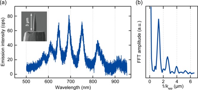
STL spectrum of a polished tip with a flat base. (a) STL spectrum obtained with the tip shown in the inset SEM image (Vbias = 2.5 V, It = 6 nA). (b) Fourier spectrum of (a) executed for the interpolated data with kspp.
In summary, we showed that near-field properties in a plasmonic STM junction can be controlled by FIB fabrication of Au tips. As an exemplary demonstration, the spectral modulation through a plasmonic Fabry–Pérot interference was examined and STL spectroscopy was used to characterize the light emission. The high degree of freedom to make nanoscale structures using FIB allows flexible control of gap plasmons in STM junctions. In addition, the STM geometry provides a unique opportunity to study remote generation of a spatially separated localized plasmon modes by tunneling electrons (as shown in Figure 4), whereby conventional diffraction-limited plasmonic couplers can be omitted. This mechanism can be incorporated in plasmonic optoelectronic devices utilizing remote excitation of surface plasmons.47−50 The control of the near-field spectral response in STM junctions also makes it possible to match the plasmonic resonance with resonances in the electronic structure of molecular systems. This is, for example, applicable to optimize resonance enhancement conditions for single-molecule spectroscopy with an optical near field.51 Moreover, near-field manipulation will also be useful to elucidate microscopic mechanisms of plasmon-assisted reactions at the single-molecule level.52 We believe that our approach paves the way for improving apertureless SNOM performance and investigating near-field physics and chemistry in (sub)nanoscale plasmonic cavities with a high degree of accuracy.
Methods
All experiments were performed in an ultrahigh vacuum (UHV) chamber (base pressure <5 × 10⁻¹⁰ mbar) equipped with a low-temperature STM (modified UNISOKU USM-1400) operated with a Nanonis SPM controller. All measurements were performed at 78 K. The bias voltage (Vbias) was applied to the sample, and the tip was grounded. The tunneling current (It) was collected from the tip. The Ag(111) surface was cleaned by repeated cycles of Ar+ sputtering and annealing up to 670 K. Light emission from the STM junction is collected by an in situ Ag-coated parabolic mirror (numerical aperture of ∼0.6) mounted on the cold STM stage and detected outside of the UHV chamber with a grating spectrometer (AndorShamrock 303i). The parabolic mirror was precisely aligned using piezo motors (Attocube GmbH), which allow three translational and two rotational motions. The focal point on the tip was adjusted by monitoring the scattering light of the incident alignment beam that is focused via the parabolic mirror. The scattered light becomes strong when the focus is either on the apex or on the groove, whereas it is significantly weaker on the smooth shaft. We further confirmed the focus at the tip apex by observing plasmon-assisted resonant tunneling,53 which is very sensitive to the local field enhancement and can be used to optimize the focus position.
The FIB fabrication of electrochemically etched Au tips was performed with an FEI Helios NanoLab G3 FIB-SEM DualBeam system and Ga ions were used for milling and the details are provided in Supporting Information.
Numerical simulations were performed to calculate the plasmonic response of the STM junction by solving the time-harmonic wave equation for the electric field within the RF-Module of COMSOL Multiphysics 5.3a. The details are provided in Supporting Information.
Acknowledgments
The authors thank M. B. Raschke, C. Ropers, and K. Busch for valuable discussions. T.K. acknowledges the support by JST-PRESTO (JPMJPR16S6). T.K. and M.W. acknowledge the support by the Deutsche Forschungsgemeinschaft through Sfb951.
Supporting Information Available
The Supporting Information is available free of charge on the ACS Publications website at DOI: 10.1021/acs.nanolett.9b00558.
FIB fabrication of the Au tips, peak position analysis in the bias voltage-dependent STML spectra, current dependence of the STML intensity for the grooved tip, numerical simulation of electromagnetic field distributions (PDF)
Author Contributions
∥ H.B. and S.L. equally contributed.
The authors declare no competing financial interest.
Supplementary Material
References
- Zayats A. V.; Smolyaninov I. I.; Maradudin A. A. Nano-optics of surface plasmon polaritons. Phys. Rep. 2005, 408, 131–314. 10.1016/j.physrep.2004.11.001. [DOI] [Google Scholar]
- Taylor A. B.; Zijlstra P. Single-Molecule Plasmon Sensing: Current Status and Future Prospects. ACS Sens. 2017, 2, 1103–1122. 10.1021/acssensors.7b00382. [DOI] [PMC free article] [PubMed] [Google Scholar]
- Atwater H. A.; Polman A. Plasmonics for improved photovoltaic devices. Nat. Mater. 2010, 9 (2010), 205–213. 10.1038/nmat2629. [DOI] [PubMed] [Google Scholar]
- Linic S.; Christopher P.; Ingram D. B. Plasmonic-metal nanostructures for efficient conversion of solar to chemical energy. Nat. Mater. 2011, 10, 911–921. 10.1038/nmat3151. [DOI] [PubMed] [Google Scholar]
- Halas N. J.; Lal S.; Chang W.-S.; Link S.; Nordlander P. Plasmons in Strongly Coupled Metallic Nanostructures. Chem. Rev. 2011, 111, 3913–3961. 10.1021/cr200061k. [DOI] [PubMed] [Google Scholar]
- Ebbesen T. W.; Lezec H. J.; Ghaemi H. F.; Thio T.; Wolff P. A. Extraordinary optical transmission through sub-wavelength hole arrays. Nature 1998, 391, 667–669. 10.1038/35570. [DOI] [Google Scholar]
- Maier S. A.Plasmonics - Fundamentals and Applications; Springer, 2007. [Google Scholar]
- Chikkaraddy R.; de Nijs B.; Benz F.; Barrow S. J.; Scherman O. A.; Rosta E.; Demetriadou A.; Fox P.; Hess O.; Baumberg J. J. Single-molecule strong coupling at room temperature in plasmonic nanocavities. Nature 2016, 535, 127–130. 10.1038/nature17974. [DOI] [PMC free article] [PubMed] [Google Scholar]
- Novotny L.; Stranick S. J. Near-field optical microscopy and spectroscopy with pointed probes. Annu. Rev. Phys. Chem. 2006, 57, 303–331. 10.1146/annurev.physchem.56.092503.141236. [DOI] [PubMed] [Google Scholar]
- Bek A.; Vogelgesang R.; Kern K. Apertureless scanning near field optical microscope with sub-10nm resolution. Rev. Sci. Instrum. 2006, 77, 043703 10.1063/1.2190211. [DOI] [PubMed] [Google Scholar]
- Pettinger B.; Schambach P.; Villagómez C. J.; Scott N. Tip-Enhanced Raman Spectroscopy: Near-Fields Acting on a Few Molecules. Annu. Rev. Phys. Chem. 2012, 63, 379–399. 10.1146/annurev-physchem-032511-143807. [DOI] [PubMed] [Google Scholar]
- Verma P. Tip-Enhanced Raman Spectroscopy: Technique and Recent Advances. Chem. Rev. 2017, 117, 6447–6466. 10.1021/acs.chemrev.6b00821. [DOI] [PubMed] [Google Scholar]
- Deckert-Gaudig T.; Taguchi A.; Kawata S.; Deckert V. Tip-enhanced Raman spectroscopy – from early developments to recent advances. Chem. Soc. Rev. 2017, 46, 4077–4110. 10.1039/C7CS00209B. [DOI] [PubMed] [Google Scholar]
- Zrimsek A. B.; Chiang N.; Mattei M.; Zaleski S.; McAnally M. O.; Chapman C. T.; Henry A.-I.; Schatz G. C.; Van Duyne R. P. Single-Molecule Chemistry with Surface- and Tip-Enhanced Raman Spectroscopy. Chem. Rev. 2017, 117, 7583–7613. 10.1021/acs.chemrev.6b00552. [DOI] [PubMed] [Google Scholar]
- Berndt R.; Gimzewski J. K.; Johansson P. Inelastic Tunneling Excitation of Tip-Induced Plasmon Modes on Noble-Metal Surfaces. Phys. Rev. Lett. 1991, 67, 3796–3799. 10.1103/PhysRevLett.67.3796. [DOI] [PubMed] [Google Scholar]
- Schneider N. L.; Berndt R. Plasmonic excitation of light emission and absorption by porphyrine molecules in a scanning tunneling microscope. Phys. Rev. B: Condens. Matter Mater. Phys. 2012, 86, 035445 10.1103/PhysRevB.86.035445. [DOI] [Google Scholar]
- Zhang Y.; Luo Y.; Zhang Y.; Yu Y.-J.; Kuang Y.-M.; Zhang L.; Meng Q.-S.; Luo Y.; Yang J.-L.; Dong Z.-C.; Hou J. G. Visualizing coherent intermolecular dipole–dipole coupling in real space. Nature 2016, 531 (2016), 623–627. 10.1038/nature17428. [DOI] [PubMed] [Google Scholar]
- Imada H.; Miwa K.; Imai-Imada M.; Kawahara S.; Kimura K.; Kim Y. Single molecule investigation of energy dynamics in a coupled plasmon-exciton system. Phys. Rev. Lett. 2017, 119, 013901 10.1103/PhysRevLett.119.013901. [DOI] [PubMed] [Google Scholar]
- Doppagne B.; Chong M. C.; Lorchat E.; Berciaud S.; Romeo M.; Bulou H.; Boeglin A.; Scheurer F.; Schull G. Vibronic Spectroscopy with Submolecular Resolution from STM-Induced Electroluminescence. Phys. Rev. Lett. 2017, 118, 127401. 10.1103/PhysRevLett.118.127401. [DOI] [PubMed] [Google Scholar]
- Zhang Y.; Meng Q.-S.; Zhang L.; Luo Y.; Yu Y.-J.; Yang B.; Zhang Y.; Esteban R.; Aizpurua J.; Luo Y.; Yang J.-L.; Dong Z.-C.; Hou J. G. Sub-nanometre control of the coherent interaction between a single molecule and a plasmonic nanocavity. Nat. Commun. 2017, 8, 15225. 10.1038/ncomms15225. [DOI] [PMC free article] [PubMed] [Google Scholar]
- Kröger J.; Doppagne B.; Scheurer F.; Schull G. Fano Description of Single-Hydrocarbon Fluorescence Excited by a Scanning Tunneling Microscope. Nano Lett. 2018, 18, 3407–3413. 10.1021/acs.nanolett.8b00304. [DOI] [PubMed] [Google Scholar]
- Doppagne B.; Chong M. C.; Bulou H.; Boeglin A.; Scheurer F.; Schull G. Electrofluorochromism at the single-molecule level. Science 2018, 361, 251–255. 10.1126/science.aat1603. [DOI] [PubMed] [Google Scholar]
- Yu A.; Li S.; Wang H.; Chen S.; Wu R.; Ho W. Visualization of Nanoplasmonic Coupling to Molecular Orbital in Light Emission Induced by Tunneling Electrons. Nano Lett. 2018, 18, 3076–3080. 10.1021/acs.nanolett.8b00613. [DOI] [PubMed] [Google Scholar]
- Aizpurua J.; Apell S. P.; Berndt R. Role of tip shape in light emission from the scanning tunneling microscope. Phys. Rev. B: Condens. Matter Mater. Phys. 2000, 62, 2065–2073. 10.1103/PhysRevB.62.2065. [DOI] [Google Scholar]
- Hoffmann G.; Aizpurua J.; Apell P.; Berndt R. Influence of tip geometry in light emission from the scanning tunnelling microscope. Surf. Sci. 2001, 482–485, 1159–1162. 10.1016/S0039-6028(00)01079-7. [DOI] [Google Scholar]
- Meguro K.; Sakamoto K.; Arafune R.; Satoh M.; Ushioda S. Origin of multiple peaks in the light emission spectra of a Au(111) surface induced by the scanning tunneling microscope. Phys. Rev. B: Condens. Matter Mater. Phys. 2002, 65, 165405. 10.1103/PhysRevB.65.165405. [DOI] [Google Scholar]
- Behr N.; Raschke M. B. Optical antenna properties of scanning probe tips: Plasmonic light scattering, tip-sample coupling, and near-field enhancement. J. Phys. Chem. C 2008, 112, 3766–3773. 10.1021/jp7098009. [DOI] [Google Scholar]
- Martínez-Blanco J.; Fölsch S. Light emission from Ag(111) driven by inelastic tunneling in the field emission regime. J. Phys.: Condens. Matter 2015, 27, 255008. 10.1088/0953-8984/27/25/255008. [DOI] [PubMed] [Google Scholar]
- Johnson P. B.; Christy R. W. Optical Constants of the Noble Metals. Phys. Rev. B 1972, 6, 4370–4379. 10.1103/PhysRevB.6.4370. [DOI] [Google Scholar]
- Ditlbacher H.; Hohenau A.; Wagner D.; Kreibig U.; Rogers M.; Hofer F.; Aussenegg F. R.; Krenn J. R. Silver Nanowires as Surface Plasmon Resonators. Phys. Rev. Lett. 2005, 95, 257403. 10.1103/PhysRevLett.95.257403. [DOI] [PubMed] [Google Scholar]
- Allione M.; Temnov V. V.; Fedutik Y.; Woggon U.; et al. Surface Plasmon Mediated Interference Phenomena in Low-Q Silver Nanowire Cavities. Nano Lett. 2008, 8, 31–35. 10.1021/nl071763o. [DOI] [PubMed] [Google Scholar]
- Dorfmüller J.; Vogelgesang R.; Weitz R. T.; Rockstuhl C.; Etrich C.; Pertsch T.; Lederer F.; Kern K. Fabry-Pérot Resonances in One-Dimensional Plasmonic Nanostructures. Nano Lett. 2009, 9, 2372–2377. 10.1021/nl900900r. [DOI] [PubMed] [Google Scholar]
- Rossouw D.; Botton G. A. Plasmonic Response of Bent Silver Nanowires for Nanophotonic Subwavelength Waveguiding. Phys. Rev. Lett. 2013, 110, 066801 10.1103/PhysRevLett.110.066801. [DOI] [PubMed] [Google Scholar]
- Temnov V. V.; Woggon U.; Dintinger J.; Devaux E.; Ebbesen T. W. Surface plasmon interferometry: measuring group velocity of surface plasmons. Opt. Lett. 2007, 32, 1235–1237. 10.1364/OL.32.001235. [DOI] [PubMed] [Google Scholar]
- Schouten H. F.; Kuzmin N.; Dubois G.; Visser T. D.; Gbur G.; Alkemade P. F. A.; Blok H.; ’t Hooft G. W.; Lenstra D.; Eliel E. R. Plasmon-Assisted Two-Slit Transmission: Young’s Experiment Revisited. Phys. Rev. Lett. 2005, 94, 053901 10.1103/PhysRevLett.94.053901. [DOI] [PubMed] [Google Scholar]
- Sain B.; Kaner R.; Bondy Y.; Prior Y. Plasmonic flat surface Fabry-Perot interferometry. Nanophotonics 2018, 7, 635–641. 10.1515/nanoph-2017-0082. [DOI] [Google Scholar]
- Bharadwaj P.; Bouhelier A.; Novotny L. Electrical Excitation of Surface Plasmons. Phys. Rev. Lett. 2011, 106, 226802. 10.1103/PhysRevLett.106.226802. [DOI] [PubMed] [Google Scholar]
- Schröder B.; Weber T.; Yalunin S. V.; Kiel T.; Matyssek C.; Sivis M.; Schäfer S.; von Cube F.; Irsen S.; Busch K.; Ropers C.; Linden S. Real-space imaging of nanotip plasmons using electron energy loss spectroscopy. Phys. Rev. B: Condens. Matter Mater. Phys. 2015, 92, 085411 10.1103/PhysRevB.92.085411. [DOI] [Google Scholar]
- Talebi N.; Sigle W.; Vogelgesang R.; Esmann M.; Becker S. F.; Lienau C.; van Aken P. A. Excitation of Mesoscopic Plasmonic Tapers by Relativistic Electrons: Phase Matching versus Eigenmode Resonances. ACS Nano 2015, 9, 7641–7648. 10.1021/acsnano.5b03024. [DOI] [PubMed] [Google Scholar]
- Guo S.; Talebi N.; Sigle W.; Vogelgesang R.; Richter G.; Esmann M.; Becker S. F.; Lienau C.; van Aken P. A. Reflection and Phase Matching in Plasmonic Gold Tapers. Nano Lett. 2016, 16, 6137–6144. 10.1021/acs.nanolett.6b02353. [DOI] [PubMed] [Google Scholar]
- Groß P.; Esmann M.; Becker S. F.; Vogelsang J.; Talebi N.; Lienau C. Plasmonic nanofocusing – grey holes for light. Adv. Phys. X 2016, 1, 297–330. 10.1080/23746149.2016.1177469. [DOI] [Google Scholar]
- Esmann M.; Becker S. F.; da Cunha B. B.; Brauer J. H.; Vogelgesang R.; Groß P.; Lienau C. k-space imaging of the eigenmodes of sharp gold tapers for scanning near-field optical microscopy. Beilstein J. Nanotechnol. 2013, 4, 603–610. 10.3762/bjnano.4.67. [DOI] [PMC free article] [PubMed] [Google Scholar]
- Maier S. A.Plasmonics: Fundamentals and Applications; Springer, 2007. [Google Scholar]
- Gay G.; Alloschery O.; Viaris de Lesegno B.; Weiner J.; Lezec H. J. Surface Wave Generation and Propagation on Metallic Subwavelength Structures Measured by Far-Field Interferometry. Phys. Rev. Lett. 2006, 96, 213901. 10.1103/PhysRevLett.96.213901. [DOI] [PubMed] [Google Scholar]
- Babadjanyan A. J.; Margaryan N. L.; Nerkararyan Kh. V. Superfocusing of surface polaritons in the conical structure. J. Appl. Phys. 2000, 87, 3785–3788. 10.1063/1.372414. [DOI] [Google Scholar]
- Stockman M. I. Nanofocusing of Optical Energy in Tapered Plasmonic Waveguides. Phys. Rev. Lett. 2004, 93, 137404. 10.1103/PhysRevLett.93.137404. [DOI] [PubMed] [Google Scholar]
- Hutchison J. A.; Centeno S. P.; Odaka H.; Fukumura H.; Hofkens J.; Uji-i H. Subdiffraction Limited, Remote Excitation of Surface Enhanced Raman Scattering. Nano Lett. 2009, 9, 995–1001. 10.1021/nl8030696. [DOI] [PubMed] [Google Scholar]
- Fang Y.; Wei H.; Hao F.; Nordlander P.; Xu H. Remote-Excitation Surface-Enhanced Raman Scattering Using Propagating Ag Nanowire Plasmons. Nano Lett. 2009, 9, 2049–2053. 10.1021/nl900321e. [DOI] [PubMed] [Google Scholar]
- Lee S. J.; Moskovits M. Remote Sensing by Plasmonic Transport. J. Am. Chem. Soc. 2012, 134, 11384–11387. 10.1021/ja3046662. [DOI] [PubMed] [Google Scholar]
- Evans C. I.; Zolotavin P.; Alabastri A.; Yang J.; Nordlander P.; Natelson D. Quantifying Remote Heating from Propagating Surface Plasmon Polaritons. Nano Lett. 2017, 17, 5646–5652. 10.1021/acs.nanolett.7b02524. [DOI] [PubMed] [Google Scholar]
- Zhang R.; Zhang Y.; Dong Z. C.; Jiang S.; Zhang C.; Chen L. G.; Zhang L.; Liao Y.; Aizpurua J.; Luo Y.; Yang J. L.; Hou J. G. Chemical mapping of a single molecule by plasmon-enhanced Raman scattering. Nature 2013, 498, 82–86. 10.1038/nature12151. [DOI] [PubMed] [Google Scholar]
- Böckmann H.; Müller M.; Hammud A.; Willinger M.-G.; Pszona M.; Waluk J.; Wolf M.; Kumagai T. Near-Field Spectral Response of Optically Excited Scanning Tunneling Microscope Junctions Probed by Single-Molecule Action Spectroscopy. J. Phys. Chem. Lett. 2019, 10, 2068–2074. 10.1021/acs.jpclett.9b00822. [DOI] [PMC free article] [PubMed] [Google Scholar]
- Liu S.; Wolf M.; Kumagai T. Plasmon-Assisted Resonant Electron Tunneling in a Scanning Tunneling Microscope Junction. Phys. Rev. Lett. 2018, 121, 226802. 10.1103/PhysRevLett.121.226802. [DOI] [PubMed] [Google Scholar]
Associated Data
This section collects any data citations, data availability statements, or supplementary materials included in this article.


