Abstract
Both experiments and simulations show that the polarization state and propagation path of the Bloch surface waves sustained on a dielectric multilayer, can be manipulated with the grooves inscribed on this multilayer. These grooves can be easily producible, accessible and controllable. Various nano-devices for the Bloch surface waves, such as the launcher, beam splitter, reflector, polarization rotator, and even the photonic single-pole double-throw switch, were all experimentally realized with the properly designed grooves, which are consistent with the numerical simulations. The proposed devices will be basic elements for the two-dimensional photonic system, and will find numerous applications, including integrated photonics, molecular sensing, imaging and micro-manipulation.
I. Introduction
Bloch surface waves (BSWs) are surface electromagnetic modes which are excited at the interface between a truncated periodic dielectric multilayer and the surrounding medium [1–3]. Similar to surface plasmon polaritons (SPPs) on a metal film [4–6], BSWs also have the intrinsic properties of enabling optical near-field confinement and enhancement, being sensitive to the environment, and having larger wave-vectors than light of the same frequency in a vacuum [7–13]. Moreover, the location of the field enhancement in dielectric multilayers can be controlled due to the resonant excitation of the surface waves [14]. Therefore, BSWs have been considered as the dielectric analogue of SPPs but with lower losses because of the lower absorption of dielectrics compared with metals. In the past decades, with the wide development of plasmonics and nanofabrication, controlled micro or nano structuration of metal surface has been proposed to work as various optical SPP elements, such as SPP-waveguides, mirrors, lenses, beam-splitters and others [15–21]. The mechanism is based on the high sensitivity of SPPs to the surface features which provides a method to control the two-dimensional propagation of SPPs [22–23]. Based on the same principles, BSWs are also very sensitive to the surface features on the top layer of the dielectric multilayer, thus many BSW devices based on two-dimensional platform have been experimental and numerically demonstrated. These two-dimensional surface wave devices are a key asset in the miniaturization of compact optical systems such as integrated photonic circuits and lab-on-a-chip devices. BSW platforms are mainly oriented to label-free sensing applications [24] where they can get competitive with respect to SPP ones, with also the possibility of simultaneous fluorescence operation mode [25]. Moreover, BSWs induced optical forces have been also demonstrated [26] and proposed for novel optical tweezers schemes. Patterning a suitable multilayer with dielectric stripes can guide the propagation of BSWs, which is to function as a BSW waveguide [27–32]. Polymer prism, gratings or other refractive structures fabricated on this multilayer can induce the reflection and diffraction of the BSWs [33, 34]. A two-dimensional lens of various shapes can focus the BSWs within subwavelength scale or to create a non-diffracting BSW [35–38], which are analogous to Bessel beams. A two-dimensional disk has been demonstrated as the resonator for BSWs [39]. Furthermore, it has been demonstrated that BSWs can strongly-couple to excitons, e.g., of a thin organic layer in order to achieve BSW polariton waves [40, 41]. These devices hence exhibit long-range propagating surface streams of hybrid photons and excitons quasi-particles, inheriting a strong nonlinearity from the latter component. For most of these reports, the BSWs are of transverse electric (TE) polarization. One of the distinct differences between SPPs and BSWs is that SPPs can only be populated in the form of transverse magnetic (TM)-polarized waves, however BSWs can be of both transverse magnetic (TM) or TE polarizations [42,43]. More polarization choices can provide more opportunities in the development of the two dimensional devices for applications in integrated photonics, sensing or imaging. In this letter, a dielectric multilayer sustaining both TM and TE polarized BSWs were fabricated. Both experiments and simulations demonstrate that various BSW devices, such as mirrors, beam splitters, polarization rotators, and even the single-pole double-throw switch, can be realized just by using the one dimensional (1D) grooves milled on the top layer of the proposed dielectric multilayer. In the present report we demonstrate that either TM or TE polarized BSW can be obtained using the same surface by selection of the grating parameters.
II. Results
A. Launching BSWs with the 1D grooves
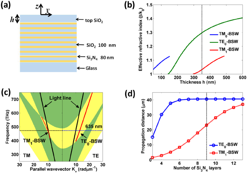
The dielectric multilayer structure is made of alternating layers of SiO2 and Si3N4, which was fabricated with plasma-enhanced chemical vapour deposition. The thicknesses of each layer are detailed in Fig. 1(a). Except for the top SiO2 layer (about 350 nm thickness), the other 8 layers of SiO2 are of about 100 nm thickness. The thickness of Si3N4 (9 layers) is about 80 nm. By using these structural parameters, both TM and TE polarized BSWs can be sustained on this multilayer. The change of the effective refractive indices of the TE-BSW and TM-BSW versus the top SiO2 layer thickness h is shown in Fig. 1(b). As the thickness h is changed from 300 to 480 nm, the dielectric multialyer can sustain the propagation for the TE0-BSW and TM1-BSW. The photonic bandgap of the dielectric multilayer and the dispersion curves for the TE0-BSW and TM1-BSW modes at the thickness h = 350 nm are shown in Fig. 1(c), respectively. From the dispersion curves, the group velocity (vg = ∂ω/∂β, β is in-plane wavevector of BSW) for the TE0-BSW and TM1-BSW at the wavelength 635 nm can be estimated as 1.783×10⁸ m/s and 1.794×10⁸ m/s, respectively. The yellow zones denote the photonic stop band of this dielectric multilayer. It is noted that the dispersion curve of TM1-BSW is closer to the band edge than that of TE0-BSW, which contributes to the deeper penetration depth for the TM1-BSW into the dielectric multilayer [1]. Then, for the dielectric multilayer with finite thickness, TM1-BSW will have larger leakage loss than that of the TE0-BSW. The propagation distance for the TE0-BSW and TM1-BSW as a function of the number of Si3N4 layers is shown in Fig. 1(d). With the increasing number of layers, the leakage loss of BSW is decreased and the propagation distance of BSW is also increased. As the number of Si3N4 layers is larger than 6, the leakage loss of the TE0-BSW is mostly inhibited and the propagation distance of TE0-BSW is not changed with increasing number of layers. To distinguish the transmission path of the TE-BSW from TM-BSW and reduce the leakage loss of TM-BSW, we used 9 pairs of SiO2-Si3N4 layers, other than our previously used 7 pairs [44, 45]. In this way, the leakage loss of the TM1-BSW is not completely inhibited, which can be observed from the glass substrate.
Figure 1. Photonic bandgap and BSW modes on a dielectric multilayer.
(a) Schematic illustration of the dielectric multilayer. The dielectric multilayer is made of 18 alternating dielectric layers of Si3N4 (80-nm-thick) and SiO2 (100-nm-thick). The thickness of top SiO2 layer can be varied and denoted as h. (b) the effective refractive indices of TE-BSW and TM-BSW modes versus the thickness h of top SiO2 layer. (c) The photonic band structure of the dielectric multilayer. The dispersion curves for the TE0-BSW and TM1-BSW are shown with red solid and dashed lines, respectively. The regions with yellow color denote the photonic band gap. (d) The propagation distance of TE0-BSW and TM1-BSW modes in the dielectric multilayer as a function of the number of Si3N4 layers. The thickness of the top SiO2 layer is fixed at 350 nm.
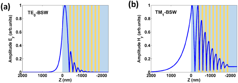
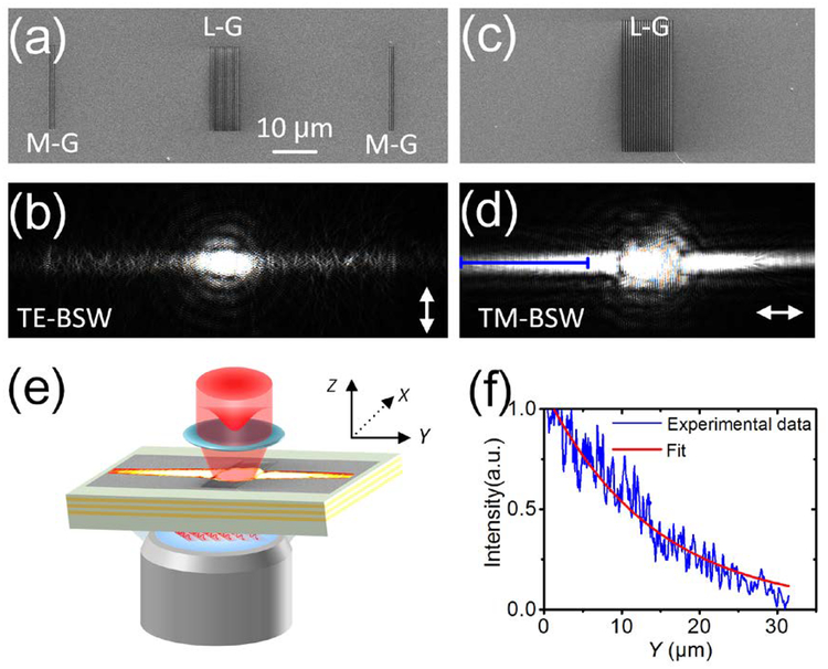
With the structural parameters used in the experiment, the electric field distributions for TE0-BSW and TM1-BSW are plotted in Fig. 2. The electric field of the TM-BSW is mainly confined inside the top dielectric layer and that of the TE-BSW is mainly on the surface of the multilayer. The effective refractive index for the TE-BSW (nTE-BSW) is 1.30, and that for the TM-BSW (nTM-BSW) is 1.03. To launch the BSW, subwavelength gratings with period equal to the effective wavelength of BSW are fabricated with a focused ion beam (FIB) on the top SiO2 layer. For the TE-BSW, the period of the launching grating (L-G) is 490 nm (= 635 nm/ 1.30), and the width and depth of the grooves are 240 nm and 150 nm, respectively, as shown in Fig. 3(a). For the TM-BSW, the period of the launching grating is 620 nm (= 635 nm/ 1.03), and the width and depth of the grooves are 300 nm and 200 nm, respectively (Fig. 3(c)). The optical field intensity distribution of the generated BSWs is then measured with a home-built leakage radiation microscope (Fig. 3(e)) [46–49]. A Gaussian beam with waist radius of 2.7 μm at a wavelength of 635 nm is focused onto the two launching gratings at an incident angle of 0° to excite BSWs. A polarizer and a half wave-plate are used to tune the incident polarization without changing the intensity of incident beam. For the TE-BSW, the polarization of the incident beam is along the orientation of the grating lines (Fig. 3(a)), and for the TM-BSW, the polarization direction is perpendicular to the grating lines (Fig. 3(c)). According to the angular spectrum decomposition of the incident Gaussian beam, the rigorous coupled-wave analysis (RCWA) is used to simulate the diffraction of incident Gaussian beam impinging on the launching grating [50]. From the simulation, the injection efficiency of Gaussian beam into the TE-BSW is about 6.18% with the geometrical parameters used in the experiment, and the injection efficiency into the TM-BSW is about 3.3%.
Figure 2. Field distributions for BSW modes on a dielectric multilayer.
(a) Normalized electric field amplitude (Ey) distribution for the TE0-BSW. (b) Normalized magnetic field amplitude (Hy) distribution for the TM1-BSW. The thickness of top SiO2 layer is fixed at 350 nm (denoted by vertical dashed line in Fig. 1(b)). The field distributions are calculated with the incident wavelength at 635 nm.
Figure 3. Launching the BSWs with grooves.
(a) SEM image of the grating for launching TE-BSW (L-G, period is 490 nm) and monitoring grooves for imaging the propagation of TE-BSW (M-G). (c) SEM image of the grating for launching TM-BSW (period is 620 nm). (b) and (d) are corresponding optical images to (a) and (c), respectively. A laser beam with wavelength at 635 nm was focused at normal incidence onto the L-G in order to launch the surface waves. The double-headed white arrows in (b and d) indicate the orientation of the incident polarization. The scale bar (10 μm) on (a) is applicable for (a-d). The grooves were inscribed on the top SiO2 layer. (e) Optical setup of the LRM. The Gaussian beam was focused onto the L-G, and then launched the BSW. The leakage radiation of the BSW is collected by the objective. (f) The blue curve line is the cross-sectional plot of (d) along the blue solid line and the red line is the corresponding exponential fitting data.
In our experiments, two monitoring grooves (M-G) were inscribed to image the TE-BSW which are on two sides of the launching grating (L-G) (Fig. 3(a)). The depth and width of the grooves of the M-G are consistent with the L-G. When the TE-BSW propagates to the monitoring grooves, its signal will be scattered by the grooves and collected by the LRM, then we can judge the propagating direction of the TE-BSWs (Fig. 3(b)), which is a commonly used method to determine the propagation path of SPPs [15]. The roughness on the surface of the dielectric multilayer will scatter the TE-BSW, which provides another route to image the propagation path, but the scattering signal is random and weak. Different from the TE-BSW, the leakage radiation signals from the TM-BSW is strong, so its propagation path can be clearly imaged with the LRM as shown in Fig. 3(d). From Figs. 3(b) and 3(d), we can find that the launched BSWs are propagating perpendicular to the gratings for both TM-BSW and TE-BSW. For SPP at an Ag/Air interface, the propagation length at a wavelength of 632.8nm is 6.4 μm [51]. For the TM-BSW in Fig. 3(d), the cross-sectional plot (Fig. 3(f)) along the blue solid line indicates that the experimental propagation length of the TM-BSW is 14.9 μm. However, the TE-BSW cannot be imaged by the LRM, and the propagation length of the experiment can’t be obtained. The calculated propagation lengths of TE-BSW and TM-BSW are about 23 μm and 40 μm as shown in Fig. 1(d), which are derived by the imaginary part of the effective refractive index of TE-BSW and TM-BSW. Thus, the propagation length of BSWs is much longer than that of the SPP, and the propagation length of TE-BSW is smilar to that of LRSPP at the same wavelength.
B. Reflector and beam splitter for BSWs made of 1D grooves
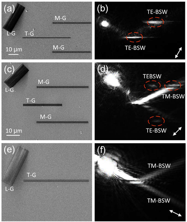
In addition to launching of TM-BSW and TE-BSW with the gratings, the propagation of BSWs can be controlled with appropriately designed grooves. As shown in Figs. 4(a) and 4(b), one groove with width, depth and length at 400 nm, 230 nm and 50 μm, was inscribed on the top SiO2 layer. We named this groove as the transforming groove (T-G). The cross-angle between the launching grating for TE-BSW and this groove is 60°, so the launched TE-BSW will strike onto this groove with the incident in-plane angle at 60°. At the position of this groove, a notable bright spot appears meaning that the TE-BSW has propagated to this groove (T-G). Above and below this groove (T-G), there are two grooves arrays named as M-G (Fig. 4(a)), which monitor the propagation of the TE-BSW. The LRM image (Fig. 4(b)) shows that there are bright spots on the top M-G, and there is no signal on the bottom M-G. This result reveals that the TE-BSW was totally reflected by the transform groove, meaning that this single groove can work as a reflector for the TE-BSW.
Figure 4. Reflector and beam splitter for BSWs.
(a) SEM image of the launching grating (L-G), the transforming groove (T-G) and the monitoring grooves (M-G), (b) corresponding optical image shows the total reflection of TE-BSW by the T-G. (c), (e) SEM images of the gratings and grooves working as the beam splitters for TE-BSW and TM-BSW, (d) and (f) the corresponding optical images of (c) and (e), respectively. The double-headed white arrows in (b, d and f) indicate the orientation of the incident polarization. The scale bar (10 μm) on (a) is applicable for (a-b), and the scale bar on (c) is applicable for (c-f).
As shown in Figs. 4(c) and 4(d), the inscribed grooves (also named as transforming grooves (T-G)) also can work as the beam splitter for the TE-BSW. Here, there are two grooves (labelled with T-G) with width and depth at 400 nm and 230 nm, respectively. The distance between the two grooves is 505 nm. The length of these two grooves is 30 μm. The incident in-plane angle of the launched TE-BSW to this T-G is set as 45°. The LRM image (Fig. 4(d)) shows that there are bright spots on both the top and bottom M-G (labelled with the ovals), which means that the TE-BSW was separated into two beams.
Similarly as the case of TE-BSW, the grooves (labelled with T-G) can also be used to divide the propagation path of the TM-BSW as presented in Fig. 4(f). In this case, two grooves are also used (Fig. 4(e)). The width and depth of each groove are 400 nm and 150 nm, respectively. The distance between two grooves is designed as 450 nm and the length of the grooves is 50 μm. The period of the launching grating (L-G) for the TM-BSW is the same as that used in Fig. 3(d). It is clearly shown that the TM-BSW has been reflected and transmitted simultaneously with the T-G (Fig. 4(f)).
C. Polarization rotator for BSWs made of 1D grooves
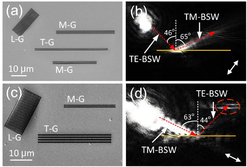
When we pay more attention on Fig. 4(d), a notable TM-BSW appears that can be attributed to the reflection of the TE-BSW by the grooves (T-G). This phenomenon indicates that the grooves can work as a polarization rotator to tune the TE-BSW into the TM-BSW [43]. To clearly show this polarization rotation of the BSWs, more experiments were carried out as shown in Fig. 5. On Fig. 5(a), the launching grating with period at 490 nm (L-G) is used for the excitation of TE-BSW, and the transforming grooves (T-G) are made of two grooves. The width and the depth of each groove are chosen to be 400 nm and 230 nm respectively. The distance between the two grooves is 410 nm. There are also two monitoring grooves (M-G) arrays above and below these transforming grooves to monitor the propagation of the launched TE-BSW. On Fig. 5(b), the propagation path of the launched TE-BSW between the launching grooves (L-G) and the transforming grooves (T-G) is invisible due to its very weak leakage radiation. But we can judge that the TE-BSW was excited and propagating to the T-G, because we can see a bright spot on the position of the T-G. From the M-G below the T-G, we have not seen any scattering signals, meaning that there is no TE-BSW transmitted through this T-G. On the other hand, at the areas between the T-G and the top M-G, we can see a distinct propagating beam. As shown in Fig. 3, the leaky radiation signals of TM-BSW is strong and thus its propagation path can be clearly imaged with the LRM. This distinct beam can be attributed to the excitation of TM-BSW. Fig. 5(b) also shows that the incident angle (θTE-BSW = 46°) of the TE-BSW is different from the reflection angle (θTM-BSW = 65°) of the TM-BSW. This anomalous reflection is due to the different effective refractive indices of the TE-BSW and TM-BSW. When the polarization of the BSW is transformed from TE to TM, its effective index will be changed, and then, the in-plane reflection angle will be different from the incident in-plane angle. Different from a bulk birefringence in 3D, which is the optical property that exsits in the optical anisotropic materials, abnormal reflection or refraction in this paper depends on the presence of TE-BSW and TM-BSW modes at the interface of M-G, and the whole sample is the isotropic material. For the dielectric multilayer photonic band gap structure used here, the effective index of the TM-BSW (nTM-BSW) is 1.03, and that of the TE-BSW (nTE-BSW) is 1.30. The relations between the in-plane incidence and reflection angle satisfy the general Snell law nTE-BSW×sin (θTE-BSW) = nTM-BSW×sin (θTM-BSW) [43].
Figure 5. Polarization rotator for BSWs.
(a), (c) SEM images of the gratings and grooves working as the polarization rotator, (b) and (d) the corresponding optical images of (c) and (e), respectively. On (a) and (b), the TE-BSW was transformed into TM-BSW during the reflection by the grooves (T-G). On (c) and (d) the TM-BSW was transformed into the TE-BSW. The double-headed white arrows in (b and d) indicate the orientation of the incident polarization. The scale bar (10 μm) on (a) is applicable for (a-b), and the scale bar on (c) is applicable for (c-d).
Additionally, the TM-BSW also can be transformed to the TE-BSW as shown in Figs. 5(c) and 5(d). Here, the launching grating with period at 620 nm is used to excite the TM-BSW. The transforming grooves (T-G) are made of 4 grooves with width and depth at 400 nm and 230 nm, respectively. The distance between adjacent grooves is 730 nm. A monitoring grooves (M-G) was fabricated on the top of the T-G, whose period, width and depth are the same as those used for launching TE-BSW. The optical image on Fig. 5(d) clearly demonstrate that the TM-BSW was excited and then encountered the T-G with the incident in-plane angle at about 63°, which was then transformed to the TE-BSW. The reflection angle of the TE-BSW is about 44°. The in-plane incidence angle and reflection angle also satisfy the general Snell law.
D. Photonic single-pole double-throw switch realized by BSWs
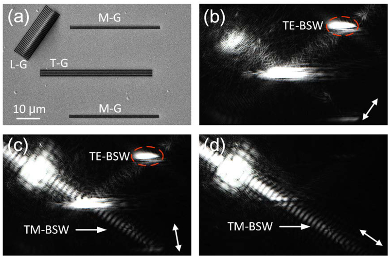
Lastly, we demonstrate that the grooves can work as a photonic single-pole double-throw switch and a polarization sensitive splitter. Different from other BSW devices in the paper, the launching grating (L-G)(Fig. 6(a)) contains two parts: the left or top part is used for the excitation of TM-BSW, and the right or below part is for TE-BSW. The launched BSW will strike to the transforming grooves (T-G) with the incident in-palne angle at 55° that is determined by the cross-angle between the L-G and the T-G. The width and depth of each groove for the T-G are 400 nm and 170 nm, respectively. The distance between adjacent grooves is 420 nm. By using these structural parameters for this T-G, the launched TE-BSW will be totally reflected without mode transformation by this T-G, and the TM-BSW will totally transmit through the T-G. As a result, the propagations of the TE-BSW and TM-BSW will be separated and the in-plane reflection angle and transmission angle are consistent with the incident in-plane angle which also satisfies the generalized Snell law. Two monitoring grooves (M-G) were fabricated above and below the T-G, respectively, which is used to monitor the propagation of the TE-BSW. The parameters of the M-G are the same as those of the launching grating for TE-BSW.
Figure 6. Photonic single-pole double-throw switch.
(a) SEM image of the gratings (L-G) and grooves (T-G and M-G). The L-G contains two parts, the top part is for the launching of TM-BSW and the bottom for TE-BSW. (b-d) the optical images with different orientations of the incident polarizations. The incident beam covers both the top and bottom parts of the L-G. The double-headed white arrows in (b and d) indicate the orientation of the incident polarization. The scale bar (10 μm) on (a) is applicable for (a-d).
By tuning the polarization direction of the linearly polarized incident free space beam that is focused onto the launching grating (L-G), the intensity of the BSWs above or below the T-G, can be tuned. For example, when the polarized direction of the incident free space beam is along the orientation of the L-G (Fig. 6(b)), only the TE-BSW is excited. Obviously BSW signal which is mostly reflected by the T-G can be viewed by the M-G above the T-G while there is only a very weak transmitted BSW through this T-G. By slightly tuning the polarization direction of the incident beam (Fig. 6(c)), the TM-BSW is then excited, which transmits through the T-G. In this case, the TE-BSW is simultaneously launched, which is reflected by the T-G and then appears on the top side of the T-G. Now, both the top side and below side of the T-G has the BSW signals. This phenomenon (Fig. 6(c)) also reveals that that this T-G works as a polarization sensitive beam splitter for the BSW.
When the polarization direction is vertical to the orientation of the L-G (Fig. 6(d)), we can find that the intensity of the BSW on the top side of the T-G is highly supressed and disappeared. On the contrary, the intensity of the BSW at the bottom of the T-G becomes strong. By comparing Figs. 6(b) and 6(d), we can find that these phenomena demonstrate the same function as that of a single-pole double-throw switch (SPDT) which has one electrically separate switch and a double-throw that has a contact can be connected to either of two contacts of the wires. It is a simple break-before-make changeover switch and is widely used in electronics. The photonic SPDT also has one incident in-plane beam and the grooves can separate the beam into two parts, either the top side or the bottom side, comparable to a SPDT switch. It also can be used as a basic element for integrated photonic circuit.
As reported in Ref. 51, the incident polarization has been used to direct the SPP beam either to the left or to the right side of the launcher. In the case of directional SPPs, the surface wave to the left and to the right of the launcher is of the same polarization (TM polarization) and cannot be changed. In our work, the BSWs directed to the top and to the bottom side of the T-G are on the same side of the launching grating (L-G), and their propagation direction is not opposite. Also, the polarizations of the two BSWs are different from each other and can be exchanged if the structural parameters are properly designed. The BSW based devices reported here can be seen as a valid alternative and complementary platform for two-dimensional optics with various design versatility, with respect to SPP based devices.
III. Discussions and numerical simulations
The mechanism of the manipulation on the BSWs’ propagation can be described as following. The effective refractive indices of both TM-BSW and TE-BSW are sensitive to the thickness of the top SiO2 layer. When a groove was inscribed on the top SiO2 layer, the effective index of the BSW inside and outside of the groove will be different from each other [43]. Then, when the BSWs strike onto the groove, reflection and refraction between two mediums (with different refractive index) will happen. By properly designing the parameters of the groove, the propagation of the BSWs can be precisely controlled. Furtherly, the reflection or transmission from different grooves can interfere constructively or destructively with each other as a standard grating, which also contribute to the propagations’ manipulation.
The mechanism of the manipulation on the polarization state is also due to the reflection and refraction of the BSWs from the grooves. Known to all, in free space optics, when a light beam undergoes reflection or refraction, its polarization will be changed. For example, we always use the effect of Brewster’s angle to generate linearly polarization light through refraction [52]. In the two dimensional-optics, this principle is the same. When the BSW of one polarization strikes onto the grooves, its reflection or refractions also can undergo the polarization changes. By properly designed grooves, the BSWs can be transformed between the TM-BSW and TE-BSW.
Based on these initial understandings of the above mechanism, numerical simulations by using the aperiodic rigorous coupled-wave analysis (ARCWA) in the conical diffraction [50, 53] have been carried out to optimize the grooves’ parameters, such as the depth, width of each grooves, the distance between adjacent grooves and so on, for the aim of realizing all the above devices. The ARCWA method analyzes a periodic structure whose adjacent periods are optically isolated. The isolation is achieved by using a perfectly matched layer (PML) along the Z axis. In the ARCWA, the effective refractive indices of the guided modes in the dielectric multilayer and the corresponding field distributions can be obtained by solving an eigen-equation [53]. The fields of the l-th mode can be expressed as
| (1) |
where denote the Fourier expansion coefficients of the electric or magnetic field for the l-th mode. Al and Bl denote the incidence and reflection coefficients of the l-th mode. The wavevector components of the l-th guided mode are given by:
| (2) |
where neff,l is the effective refractive index for the l-th guided mode. θinc is the incidence angle of the BSW. m is the Fourier expansion order used in the ARCWA. L is the periodicity of calculation domain. Then, according to the continuity boundary condition for transverse field, the fields inside and outside of grooves are correlated. Finally, the diffraction properties of BSW propagating across the grooves will be obtained by solving the coefficients Al and Bl. In our simulation, a periodicity L =10 μm and total 261 Fourier expansion orders are chosen to ensure the convergence of the results.
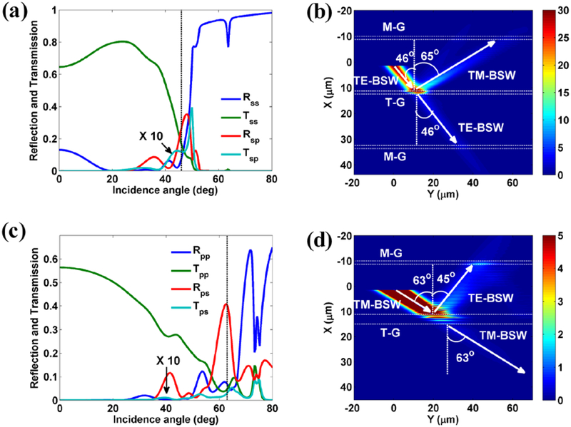
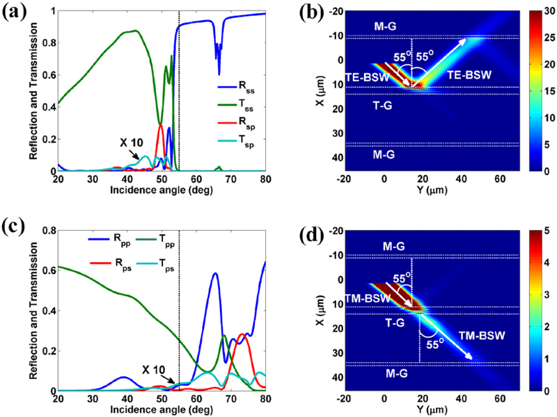
In the simulations, if the incident wave is TE-BSW, Rss and Tss denote the in-plane reflectivity and transmissitivity of TE-BSW, Rsp and Tsp denote the reflection and transmission efficiency of TM-BSW which are excited by the incident TE-BSW. Similarly, if the incident wave is TM-BSW, Rpp and Tpp denote the in-plane reflectivity and transmissitivity of TM-BSW, Rps and Tps denote the reflection and transmission efficiency of TE-BSW excited by the TM-BSW. Due to that the length of transforming and monitoring grooves in the structure are much larger than the wavelength of light, the diffraction effect of light along the direction parallel to the grooves is not considered. Then, the grooves can be considered with the one-dimensional (1D) structure in the simulations. In simulation, the refractive indices of SiO2, Si3N4, and glass are 1.48 + i0.001, 2.65 + i0.005, and 1.515, respectively. To simulate the near field distributions for the functional devices of BSW, the incident BSW is also modelled as a Gaussian shape. The Gaussian BSW beam is simulated using the angular spectrum decomposition, which can be solved in the ARCWA.
Besides the incidence angle, the depth and width of the groove can also affect the mode conversion efficiency and the scattering loss of BSW [43]. As the TE-BSW propagates across the groove, the scattering loss of TE-BSW is defined as
| (3) |
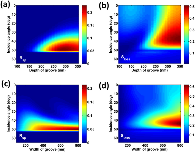
As the width of the groove is first fixed at 400 nm, the mode conversion efficiency Rsp and the scattering loss Sloss of TE-BSW versus the depth of groove and incidence angle are shown in Figs. 7(a) and 7(b), respectively. As the depth of the groove is smaller than 150 nm, the mode conversion efficiency and the scattering loss of the TE-BSW are very small. With the increasing of the depth of the groove, the Rsp is increased, but the Sloss of the TE-BSW is also increased. To balance the efficiency of mode conversion and the scattering loss of TE-BSW, the depth of the groove is chosen to be 230 nm. In addition, the relationship of mode conversion efficiency Rsp and the scattering loss Sloss of the TE-BSW between the width of groove and incidence angle are shown in Figs. 7(c) and 7(d), respectively. As the width of the groove is larger than 200 nm, the mode conversion of the TE-BSW becomes insensitive to the changes of groove width. Moreover, the scattering loss of the TE-BSW will increase as the width of groove is larger than 400 nm. Therefore, the depth and width of the groove are chosen as 230 nm and 400 nm in the experiment to balance the mode conversion efficiency and the scattering loss of the BSW. Moreover, the reflection, transmission and the mode conversion of BSW propagating across multiple grooves can be analysized by using the generalized Fresnel formula [43].
Figure 7. The influence of geometrical parameters of groove on the mode conversion of the BSW.
(a) the mode conversion efficiency Rsp, and (b) the scattering loss of TE-BSW as a function of incidence angle and the depth of groove. The width of groove is fixed at 400 nm. As the depth of groove is fixed at 230 nm, (c) the mode conversion efficiency Rsp, and (d) the scattering loss of TE-BSW as a function of incidence angle and the width of groove.
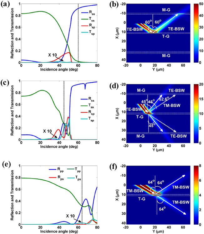
In the following simulations, the structural parameters of all the grooves and dielectric multilayer are the same as those used in the above experiments, respectively. In Fig. 8, the calculated reflectivity and transmissivity of the BSWs by the grooves of corresponding structural parameters are shown. As the incidence angle of TE-BSW is larger than 60° (denoted by vertical dashed line in Fig. 8(a)), the reflectivity of TE-BSW approaches to one. It means that the single groove can be used as a mirror for TE-BSW (Fig. 8(b)). As the incidence angle of TE-BSW is equal to 45° (denoted by vertical dashed line in Fig. 8(c)), the reflectivity of TE-BSW is equal to that of the transmissivity, i.e., Rss = Tss. Then, the grooves can work as a 50:50 beam splitter for TE-BSW (Fig. 8(d)). As the incidence angle of TM-BSW is fixed at 64° (denoted by vertical dashed line in Fig. 8(e)), the reflectivity of TM-BSW is equal to that of the transmissivity, i.e., Rpp = Tpp. Then, the grooves (T-G) can work as a 50:50 beam splitter for the TM-BSW (Fig. 8(f)).
Figure 8. Reflection and transmission of BSWs by the grooves.
(a) The reflection, transmission and mode conversion efficiencies of TE-BSW propagating across a single groove versus the in-plane incidence angle. (b) The electric field intensity distribution for the TE-BSW when it strikes to the grooves (T-G) with incidence angle at 60°. (c) The reflection, transmission and mode conversion efficiencies of TE-BSW propagating across two grooves versus the incidence angle. (d) The electric field intensity distribution for TE-BSW when it strikes to the grooves (T-G) with incidence angle at 45°. (e) The reflection, transmission and mode conversion efficiencies of TM-BSW propagating across two grooves versus the incidence angle. (f) The electric field intensity distribution for the TM-BSW when it strikes to the grooves (T-G) with incidence angle 64°. The white dashed lines parallel to the Y axis in (b), (d) and (f) denote the exterior boundaries of monitoring and transforming grooves (M-G and T-G). The mode conversion efficiencies of Tsp and Tps (shown in (a), (c) and (e)) are magnified by a factor of 10. The structural parameters of all the grooves and dielectric multilayer are the same as those used in the experiments (Fig. 4), respectively.
The simulated mode transformations between TM-BSW and TE-BSW (or polarization transformation of BSWs) are presented in Fig. 9. On the reflection part of Fig. 9(b), the TM-BSW appears meaning that the TE-BSW is transformed to TM-BSW due to reflection by the T-G. Similarly, on the reflection part of Fig. 9(d), the TE-BSW appears meaning that the TM-BSW is transformed to TE-BSW due to reflection by the T-G.
Figure 9. Modes transformation between TM-BSW and TE-BSW.
(a) The reflection, transmission and mode conversion efficiencies of TE-BSW propagating across two grooves versus the incidence angle. (b) The electric field intensity distribution for the BSW when the TE-BSW strikes to the transforming grooves (T-G) with incidence angle at 46° (denoted by vertical dashed line in (a)). (c) The reflection, transmission and mode conversion efficiencies of TM-BSW propagating across four grooves versus the incidence angle. (d) The electric field intensity distribution for the BSW when the TM-BSW strikes to the transforming grooves (T-G) with incidence angle at 63° (denoted by vertical dashed line in (c)). The white dashed lines parallel to the Y axis in (b) and (d) denote the exterior boundaries of the T-G and M-G. The mode conversion efficiencies of Tsp and Tps (shown in (a) and (c)) are magnified by a factor of 10. The structural parameters of all the grooves and dielectric multilayer are the same as those used in the experiments (Fig. 5), respectively.
The polarization sensitive beam splitter for BSWs made of grooves is also simulated as shown in Fig. 10. Here, the T-G on Figs. 10(b) and 10(d) are of the same structural parameters (width, depth, gap between grooves) as those used in experiment (Fig. 6). The incident angle for TE-BSW and TM-BSW is also the same (55°). The TE-BSW will be reflected (Fig. 10(b)) and the TM-BSW will be transmitted (Fig. 10(d)), which are consistent with the experimental results shown in Fig. 6. So these phenomena verify that the transforming grooves (T-G) can work as the polarization sensitive beam splitter for BSW, and then can be used for the development of photonic single-pole double-throw switch.
Figure 10. Polarization-sensitive beam splitter for BSWs.
(a) the reflection, transmission and mode conversion efficiencies of TE-BSW propagating across four grooves versus the incidence angle. (b) The electric field intensity distribution for TE-BSW with incidence angle 55° , which shows the total reflection of the TE-BSW by the transforming grooves (T-G). (c) The reflection, transmission and mode conversion efficiencies of TM-BSW propagating across four grooves versus the incidence angle. (d) The electric field intensity distribution for TM-BSW when it strikes at the T-G with incidence angle 55°. The white dashed lines parallel to the Y axis in (b) and (d) denote the exterior boundaries of monitoring and transforming grooves. The mode conversion efficiencies of Tsp and Tps (shown in (a) and (c)) are magnified by a factor of 10. The structural parameters of all the grooves and dielectric multilayer are the same as those used in the experiments (Fig. 6), respectively.
IV. Summary
In summary, both experimental results and numerical simulations show that the propagation and polarization of BSWs can be controlled with properly designed grooves fabricated on a dielectric multilayer photonic band gap structure. Thus, these grooves can work as the launcher and monitoring elements, as well as functional elements such as reflector and polarization sensitive beam splitters for two dimensional waves. Different from the SPPs which can be populated only in TM-polarization, the BSWs can be sustained in two polarization states (TM-BSW and TE-BSW). These grooves can also works as the polarization rotator for TM-BSW and TE-BSW. The conversion between these two BSWs provides a simple method to tune the polarization and electric field distributions of the two-dimensional waves, which may has potential applications in molecular sensing or imaging, and also will provide opportunities in exploring the interactions between two-dimensional waves and the hotly investigated two-dimensional materials [54]. The reason is that both molecules and two-dimensional materials may be sensitive to the polarization of the illumination surface waves. What is more, due to the co-existence of TM-BSW and TE-BSW, the photonic single-pole double-throw switch has been realized. It should be noted, the proposed method on manipulating the propagation and the polarization is also applicable to other planar waveguide containing two modes [55]. Thus our work provides a general approach on how to realize two-dimension photonic devices for a lab-on-a-chip, optical computing, or applications which have not yet been identified.
Acknowledgements
This work was supported by MOST (2016YFA0200601 and 2013CBA01703), NSFC (61427818, 11774330), the Science and Technological Fund of Anhui Province for Outstanding Youth (1608085J02), the Longshan academic talent research supporting program of SWUST (18LZX539), and the Fundamental Research Funds for the Central Universities (WK2030380008). This work was also supported by grants from the National Institute of Health (GM125976 and OD019975). This work was partially carried out at the University of Science and Technology of China’s Center for Micro and Nanoscale Research and Fabrication. We thank Haitao Liu, Xiaolei Wen, Linjun Wang, and Yu Wei for their help on the micro/nano fabrication steps.
References
- [1].Yeh P, Yariv A, and Hong CS, Electromagnetic propagation in periodic stratified media. I. General theory, J. Opt. Soc. Am 67, 423–438 (1977). [Google Scholar]
- [2].Joannopoulos JD, Johnson SG, Winn JN, and Meade RD, Photonic Crystals: Molding the Flow of Light, Princeton University Press, 2008. [Google Scholar]
- [3].Yu L, Barakat E, Sfez T, Hvozdara L, Di Francesco J, and Herzig HP, Manipulating Bloch Surface Waves In 2D: A Platform Concept-Based Fat Lens, Light: Sci. Appl 3,124/1–7 (2014). [Google Scholar]
- [4].Barnes WL, Dereux A, and Ebbesen TW, Surface Plasmon Subwavelength optics, Nature, 424, 824–830 (2003). [DOI] [PubMed] [Google Scholar]
- [5].Raether H, Surface Plasmons on Smooth and Rough Surfaces and on Gratings, Springer-Verlag, Berlin, 1988. [Google Scholar]
- [6].Polo JA, Mackay TG, and Lakhtakia A, Electromagnetic Surface Waves. A Modern Perspective, Elsevier, New York, 293 (2013). [Google Scholar]
- [7].Lereu AL, Zerrad M, Passian A, and Amra C, Surface plasmons and Bloch surface waves: Towards optimized ultra-sensitive optical sensors, Appl. Phys. Lett 111, 011107 (2017). [Google Scholar]
- [8].Soboleva I, Descrovi E, Summonte C, Fedyanin A, and Giorgis F, Fluorescence emission enhanced by surface electromagnetic waves on one-dimensional photonic crystals, Appl. Phys. Lett 94, 231122 (2009). [Google Scholar]
- [9].Li Y, Yang T, Song S, Pang Z, Du G, and Han S, Phase properties of Bloch surface waves and their sensing applications, Appl. Phys. Lett 103, 041116 (2013). [Google Scholar]
- [10].Paeder V, Musi V, Hvozdara L, Herminjard S, and Herzig H, Detection of protein aggregation with a Bloch surface wave based sensor, Sens. Actuators B Chem 157, 260–26 (2011). [Google Scholar]
- [11].Giorgis F, Descrovi E, Summonte C, Dominici L and Michelotti F, Experimental determination of the sensitivity of Bloch surface waves based sensors, Opt. Express 18, 8087–8093(2010). [DOI] [PubMed] [Google Scholar]
- [12].Delfan A, Liscidini M, and Sipe JE, Surface enhanced Raman scattering in the presence of multilayer dielectric structures, J. Opt. Soc. Am. B 29, 1863–1874 (2012). [Google Scholar]
- [13].Romodina M, Soboleva I, Musorin A, Nakamura Y, Inoue M, and Fedyanin AA, Bloch-surface-wave-induced Fano resonance in magneto photonic crystals, Phys. Rev. B 96, 081401(2017). [Google Scholar]
- [14].Amra C, Zerrad M, Lemarchand F, Lereu A, Passian A, Zapien JA, and Lequime M, Energy density engineering via zero-admittance domains in all-dielectric stratified materials, Phys. Rev. A 97,023819 (2018). [Google Scholar]
- [15].González MU, Weeber J-C, Baudrion A-L, Dereux A, Stepanov AL, Krenn JR, Devaux E, and Ebbesen TW, Design, Near-field Characterization, and Modeling of 45° Surface-Plasmon Bragg Mirrors, Phys. Rev. B 73, 155416 (2006). [Google Scholar]
- [16].Randhawa S, González M, Renger J, Enoch S, and Quidant R, Design and Properties of Dielectric Surface Plasmon Bragg Mirrors, Opt. Exp, 18, 14496–14510 (2010). [DOI] [PubMed] [Google Scholar]
- [17].Devaux E, Ebbesen TW, Weeber JC, and Dereux A, Launching and Decoupling Surface Plasmons via Micro-gratings, Appl. Phys. Lett 83, 4936 (2003). [Google Scholar]
- [18].Ditlbacher H, Krenn JR, Schider G, Leitner A, and Aussenegg FR, Two-Dimensional Optics with Surface Plasmon Polaritons, Appl. Phys. Lett 81, 1762 (2002). [Google Scholar]
- [19].Hohenau A, Krenn JR, Stepanov AL, Drezet A, Ditl-bacher H, Steinberger B, Leitner A, and Aussenegg FR, Dielectric Optical Elements for Surface Plasmons, Opt. Lett 30, 893–895 (2005). [DOI] [PubMed] [Google Scholar]
- [20].Kitson SC, Barnes WL, and Sambles JR, Full Photonic Band Gap for Surface Modes in the Visible, Phys. Rev. Lett 77, 2670–2673 (1996). [DOI] [PubMed] [Google Scholar]
- [21].Bozhevolnyi SI, Erland J, Leosson K, Skovgaard PMW, and Hvam JM, Waveguiding in Surface Plasmon Polariton Band Gap Structures, Phys. Rev. Lett 86, 3008–3011 (2001). [DOI] [PubMed] [Google Scholar]
- [22].Shchegrov AV, Novikov IV, and Maradudin AA, Scattering of Surface Plasmon Polaritons by a Circularly Symmetric Surface Defect, Phys. Rev. Lett 78, 4269–4272 (1997). [Google Scholar]
- [23].Seidel J, Baida FI, Bischoff L, Guizal B, Grafström S, VanLabeke D, and Eng LM, Coupling Between Surface Plasmon Modes on Metal Films, Phys. Rev. B 69, 121405(R) (2004) [Google Scholar]
- [24].Sinibaldi A, Danz N, Descrovi E, Munzert P, Schulz U, Sonntag F, Dominici L, and Michelotti F, Direct Comparison of the Performance of Bloch Surface Wave and Surface Plasmon Polariton Sensors, Sensor. Actuat. B-Chem 174, 292–298 (2012). [Google Scholar]
- [25].Sinibaldi A, Fieramosca A, Rizzo A, Riccardo R, Anopchenko A, Danz N, Munzert P, Magistris C, Barolo C, and Michelotti F, Combining Label-free and Fluorescence Operation of Bloch Surface Wave Optical Sensors, Opt. Lett 39 (10), 2947–2950 (2014). [DOI] [PubMed] [Google Scholar]
- [26].Shilkin DA, Lyubin EV, Soboleva IV, and Fedyanin AA, Direct measurements of forces induced by Bloch surface waves in a one-dimensional photonic crystal, Opt. Lett 40 (21), 4883–4886 (2015). [DOI] [PubMed] [Google Scholar]
- [27].Descrovi E, Sfez T, Quaglio M, Brunazzo D, Dominici L, Michelotti F, Herzig HP, Martin OJ, and Giorgis F, Guided Bloch Surface Waves on Ultrathin Polymeric Ridges, Nano Lett 10, 2087–2091 (2010). [DOI] [PubMed] [Google Scholar]
- [28].Abrashitova KA, Gulkin DN, Safronov KR, Kokareva NG, Antropov IM, Bessonov VO, and Fedyanin AA, Bloch Surface Wave Photonic Device Fabricated by Femtosecond Laser Polymerisation Technique, Appl. Sci 8, 63 (2018). [Google Scholar]
- [29].Sfez T, Descrovi E, Yu L, Brunazzo D, Quaglio M, Dominici L, Nakagawa W, Michelotti F, Giorgis F, Martin OJ, et al. , Bloch surface waves in ultrathin waveguides: Near-field investigation of mode polarization and propagation, J. Opt. Soc. Am. B 27, 1617–1625 (2010). [Google Scholar]
- [30].Yu L, Barakat E, Nakagawa W and Herzig HP, Investigation of ultra-thin waveguide arrays on a Bloch surface wave platform, J. Opt. Soc. Am. B 31, 2996–3000 (2014). [Google Scholar]
- [31].Wang R, Xia H, Zhang D, Chen J, Zhu L, Wang Y, Yang E, Zang T, Wen X, Zou G, et al. , Bloch surface waves confined in one dimension with a single polymeric nanofibre, Nat. Commun 8, 14330 (2017). [DOI] [PMC free article] [PubMed] [Google Scholar]
- [32].Sfez T, Descrovi E, Dominici L, Nakagawa W, Michelotti F, Giorgis F, and Herzig HP, Near-field analysis of surface electromagnetic waves in the bandgap region of a polymeric grating written on a one-dimensional photonic crystal, Appl. Phys. Lett 93, 61108 (2008). [Google Scholar]
- [33].Yu L, Barakat E, Di Francesco J, and Herzig HP, Two-dimensional polymer grating and prism on Bloch surface waves platform, Opt. Exp 23, 31640–31647 (2015). [DOI] [PubMed] [Google Scholar]
- [34].Sfez T, Descrovi E, Yu L, Quaglio M, Dominici L, Nakagawa W, Michelotti F, Giorgis F, and Herzig HP, Two-dimensional optics on silicon nitride multilayer: Refraction of Bloch surface waves. Appl. Phys. Lett 96, 151101 (2010) [Google Scholar]
- [35].Kim M-S, Dubey R, Barakat E, and Herzig HP, Nano-Thin 2D Axicon Generating Nondiffracting Surface Waves. 2016 International Conference on Optical Mems and Nanophotonics (OMN); Singapore, M02.10–1/3 (2016). [Google Scholar]
- [36].Kim M-S, Vosoughi Lahijani B, Descharmes N, Straubel J, Negredo F, Rockstuhl C, Hayrinen M, Kuittinen M, Roussey M, and Herzig HP, Subwavelength Focusing of Bloch Surface Waves, ACS Photonics 4, 1477–1483 (2017). [Google Scholar]
- [37].Angelini A, Lamberti A, Ricciardi S, Frascella F, Munzert P, De Leo N, and Descrovi E, In-plane 2D focusing of surface waves by ultrathin refractive structures, Opt. Lett 39, 6391–6394 (2014). [DOI] [PubMed] [Google Scholar]
- [38].Kim M-S, Lahijani B. Vosoughi, and Herzig HP, Stepwise Luneburg Lens for Bloch Surface Waves, Appl. Sci 8, 245 (2018). [DOI] [PMC free article] [PubMed] [Google Scholar]
- [39].Dubey R, Lahijani BV, Barakat E, Häyrinen M, Roussey M, Kuittinen M, and Herzig HP, Near-field characterization of a Bloch-surface-wave-based 2D disk resonator, Opt. Lett 41, 4867–4870 (2016). [DOI] [PubMed] [Google Scholar]
- [40].Lerario G, Cannavale A, Ballarini D, Dominici L, Giorgi MD, Liscidini M, Gerace D, Sanvutto D, and Gigli G, Room temperature Bloch Surface Wave Polaritons, Opt. Lett 39(7), 2068–2071 (2014). [DOI] [PubMed] [Google Scholar]
- [41].Lerario G, Ballarini D, Fieramosca A, Cannavale A, Genco A, Mangione F, Ganbino S, Dominici L, Giorgi MD, Gigli G, and Sanvutto D, High-speed flow of interacting organic polarizations, Light: Sci. Appl 6, e16212 (2017). [DOI] [PMC free article] [PubMed] [Google Scholar]
- [42].Gao J, Sarangan AM, and Zhan Q, Polarization Multiplexed Fluorescence Enhancer using a Pixelated One-Dimensional Photonic Band Gap Structure, Opt. Lett 37, 2640–2642 (2012). [DOI] [PubMed] [Google Scholar]
- [43].Chen JX, Zhang DG, Wang P, Ming H, and Lakowicz JR, Strong Polarization Transformation of Bloch Surface Waves, Phys. Rev. Appl 9, 024008–1/10 (2018). [DOI] [PMC free article] [PubMed] [Google Scholar]
- [44].Wang RX, Wang Y, Zhang DG, Si GY, Zhu LF, Du LP, Kou SS, Badugu R, Rosenfeld M, Lin J, Wang P, Ming H, Yuan XC, and Lakowicz JR, Diffraction-Free Bloch Surface Waves, ACS Nano 11, 5383–5390 (2017). [DOI] [PMC free article] [PubMed] [Google Scholar]
- [45].G Zhang D, Wang RX, Xiang YF, Kuai Y, Kuang CF, Badugu R, Xu YK, Wang P, Ming H, Liu X, and Lakowicz JR, Silver Nanowires for Reconfigurable Bloch Surface Waves, ACS Nano, 11 (10), 10446–10451 (2017). [DOI] [PMC free article] [PubMed] [Google Scholar]
- [46].Zhang DG, Yuan XC, Yuan GH, Wang P, and Ming H, Directional Fluorescence Emission Characterized with Leakage Radiation Microscopy, J. Opt 12, 035002/1–4 (2010). [Google Scholar]
- [47].Descrovi E, Barakat E, Angelini A, Munzert P, De Leo N, Boarino L, Giorgis F, and Herzig HP, Leakage radiation interference microscopy, Opt. Lett 38, 3374–3376 (2013). [DOI] [PubMed] [Google Scholar]
- [48].Drezet A, Hohenau A, Stepanov AL, Ditlbacher H, Steinberger B, Galler N, Aussenegg FR, Leitner A, and Krenn JR, How to erase surface plasmon fringes, Appl. Phys. Lett 89, 091117 (2006). [Google Scholar]
- [49].Massenot S, Grandidier J, Bouhelier A, Colas des Francs G, Markey L, Weeber JC, Dereux A, Renger J, Gonzàlez M, and Quidant R, Polymer-metal waveguides characterization by Fourier plane leakage radiation microscopy, Appl. Phys. Lett 91, 243102 (2007). [Google Scholar]
- [50].Moharam MG, Gaylord TK, Grann EB, and Pommet DA, Formulation for stable and efficient implementation of the rigorous coupled-wave analysis of binary gratings, J. Opt. Soc. Am. A 12, 1068–1076 (1995). [Google Scholar]
- [51].Lin J, Mueller JP, Wang Q, Yuan GH, Antoniou N, Yuan XC, and Capasso F, Polarization-controlled tunable directional coupling of surface plasmon polaritons, Science 340, 331–334 (2013). [DOI] [PubMed] [Google Scholar]
- [52].Born M. and Wolf E, Principles of Optics, 7th edition Cambridge University Press, 1999. [Google Scholar]
- [53].Silberstein E, Lalanne P, Hugonin JP, and Cao Q, Use of grating theories in integrated optics. J. Opt. Soc. Am. A 18, 2865–2875 (2001). [DOI] [PubMed] [Google Scholar]
- [54].Lerario G, Ballarini D, Dominici L, Fieramosca A, Cannavale A, Holwill M, Kozikov A, Novoselov KS, and Gigli G, Bloch Surface Waves for MoS2 Emission Coupling and Polarization Systems, App. Sci 7(12), 1217 (2017). [Google Scholar]
- [55].Wang RX, Zhang DG, Zhu LF, Wen XL, Chen JX and Kuang CF, Liu X, Wang P, Ming H, Badugu R, and Lakowicz JR, Selectable Surface and Bulk Fluorescence Imaging with Plasmon-Coupled Waveguides, J. Phys. Chem. C 119, 22131–22136 (2015). [DOI] [PMC free article] [PubMed] [Google Scholar]


