Abstract
We introduce a novel concept for the design of functional surfaces of materials: Spatial surface charge engineering. We exploit the concept for an all-solid-state, epitaxial InN/InGaN-on-Si reference electrode to replace the inconvenient liquid-filled reference electrodes, such as Ag/AgCl. Reference electrodes are universal components of electrochemical sensors, ubiquitous in electrochemistry to set a constant potential. For subtle interrelation of structure design, surface morphology and the unique surface charge properties of InGaN, the reference electrode has less than 10 mV/decade sensitivity over a wide concentration range, evaluated for KCl aqueous solutions and less than 2 mV/hour long-time drift over 12 hours. Key is a nanoscale charge balanced surface for the right InGaN composition, InN amount and InGaN surface morphology, depending on growth conditions and layer thickness, which is underpinned by the surface potential measured by Kelvin probe force microscopy. When paired with the InN/InGaN quantum dot sensing electrode with super-Nernstian sensitivity, where only structure design and surface morphology are changed, this completes an all-InGaN-based electrochemical sensor with unprecedented performance.
Subject terms: Materials science, Nanoscience and technology
Introduction
Electrochemical electrodes are prime examples of materials with functional surfaces. One of their key applications is as electrochemical sensors. Electrochemical sensors are used in medical diagnostics1,2, environmental monitoring3,4, food safety analysis5, industrial process control6 and bio-defense7. They are conceptually robust, fast, simple to use on-site in real-time and cheap. Every electrochemical sensor, amperometric8 or potentiometric9,10, requires a reference electrode next to the sensing electrode11–14 to set a constant potential. While there are many robust, all-solid-state solutions for the sensing electrode, the reference electrode almost always is the liquid-filled Ag/AgCl electrode. It consists of a chlorinated Ag wire immersed in a saturated KCl solution, which is in contact with the analyte solution through a porous material. Such electrodes are bulky and difficult to miniaturize. They are not compatible with planar device fabrication technology, have a limited lifetime and need cumbersome maintenance. Conventional liquid-filled reference electrodes need to be replaced for realizing compact and robust electrochemical sensors and sensor arrays. Simply using inert noble metal wires of Ag or Pt15,16 as quasi-reference electrodes does not result in a stable response. More promising is the reduction of the sensitivity of all-solid-state sensing electrodes through passivation of active sites using, e.g., silanes17, PVC18 or polypyrrole19. However, reduction of the sensitivity to a target below 10 mV/decade of analyte concentration with acceptable drift below 5 mV/hour is difficult.
In search for the best materials, InGaN has recently been uncovered for electrochemical sensor electrodes due to its high chemical stability, non-toxicity and bio-compatibility20–22. In addition, InN/InGaN quantum dot (QD) ion- and bio-sensing electrodes have been discovered with unprecedented, super-Nernstian potentiometric response23–26. The superior performance has been assigned to the presence of a high density of intrinsic, positively charged donor states on the InN surface27,28 together with the zero-dimensional electronic properties of the QDs26. These sensing electrodes have been operated together with conventional Ag/AgCl reference electrodes, limiting the realization of compact sensor devices.
Here we demonstrate a stable, all-solid-state, epitaxial InN/InGaN-on-Si reference electrode upon a sophisticated interplay of structure design, surface morphology and surface charge. Such an all-solid-state reference electrode allows compact and robust, easy to maintain all-solid-state miniaturized sensors and sensor arrays, removing all the difficulties associated with liquid-filled reference electrodes. The basic idea is to create a surface with balanced surface charge distribution at the nanoscale, i.e., balanced nanoscale regions with positive and negative surface charge, such that a stable, analyte concentration insensitive response originates. This exploits the unique surface properties of InGaN: (i) transition from negatively to positively charged surface states at about 45% In content for the c-plane, reaching a density of 2 × 1013 cm−2 for InN29,30 and (ii) negatively charged surface states for the m-plane over the entire In composition range28. The parameters for electrode construction at hand are the In content of the InGaN layer, the amount of deposited InN and the InGaN surface morphology, which is determined by the growth conditions (growth temperature and V-III flux ratio) and layer thickness. For the right parameters the reference electrode exhibits less than 10 mV/decade potential response over a wide concentration range from 0.001 to 1 M KCl aqueous solutions and less than 2 mV/hour long-time potential drift over 12 hours in 0.1 M KCl aqueous solution. The delicate interplay of structure, morphology and surface charge for the electrochemical response is underpinned by measurements of the relative surface potential by Kelvin probe force microscopy (KPFM). This introduces the concept of spatial surface charge engineering for achieving the desired surface functionality. By solely modifying structure and morphology and, hence, surface charge distribution, the highly sensitive InN/InGaN QD sensing electrode is obtained, complementing the concept.
In a broader view, next to epitaxial III-V semiconductor heterostructures, surface and interface engineering also plays an important role in improving the properties of the heterostructures of metal oxides, two-dimensional materials and nanoparticles. As for epitaxial III-V semiconductors and specifically nitride semiconductors26,31,32, applications include catalysis33,34, photovoltaics35, memories36,37, and photodetectors38–43. Various combinations of different materials have been realized and design parameters include doping, lattice matching, energy band matching and metal particle decoration. Certainly these approaches provide complementary solutions.
For reference electrode fabrication, facing a vast amount and combinations of available parameters, we pre-select an In content of the InGaN layer of 45%, where a charge neutral c-plane surface with concentration insensitive but unstable response is expected. InGaN layers with lower or higher In content exhibit strong response due to a high density of either negatively or positively charged surface states. In particular this has been reported for pure GaN and InN layers22. We discuss only samples fabricated at a growth temperature close to the InGaN decomposition temperature and with close-to-stoichiometric V-III flux ratio, as only these conditions lead to surface morphologies with concentration independent response. Planar InN/InGaN layers grown on GaN/sapphire substrates always show strong response23–25. Hence, the key parameters explicitly highlighted are the InN coverage and the thickness of the InGaN layer grown on Si. Doping might be another design parameter, however, because of the high n-type conductivity of the InGaN layers due to a high density of defects, acting as donors, doping is expected to have minor influence. On the other hand, these defects do not appear detrimental for the functionality of the electrodes, which is purely surface related. Best parameter identification is done for cycling in 0.1 and 1 M KCl aqueous solutions. The best candidate is then evaluated over a wide concentration range and long time.
Results
OCP as function of InN deposition amount
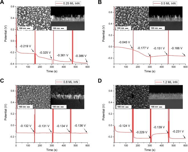
Figure 1 shows the open circuit potential (OCP) as a function of time for the InN/InGaN samples with 95 nm thick InGaN layers and 0.25 (Fig. 1A), 0.5 (Fig. 1B), 0.8 (Fig. 1C) and 1.2 (Fig. 1D) monolayer (ML) InN deposition amount. The InN/InGaN samples are alternately immersed for 150 seconds in 0.1 and 1 M KCl aqueous solutions. The insets show the top-view scanning electron microscopy (SEM) images (left-hand side) and cross-sectional SEM views (right-hand side) of the respective InN/InGaN structures. The cross-sectional images reveal dense, columnar growth with the columns touching and eventually coalescing. On the sample surfaces this translates into an undulated surface morphology, seen in top-view SEM. Within develop individual, isolated columns, which are distributed randomly. This is due to the complex nucleation behavior of In-rich InGaN directly on Si, which is not discussed further here. The InN layers cannot be distinguished on these non-planar surfaces. For the 0.25 and 0.5 ML InN layers, the OCP shows a weak potential response directly after immersing the InN/InGaN samples into the KCl solutions with different concentrations. Afterwards, however, there is a large drift. This drift is strongly reduced for the 0.8 ML InN layer, being a good candidate for a reference electrode. To note, the 0.25, 0.5 and 0.8 ML InN coverages are below or just at the critical thickness for QD formation on planar InGaN layers grown on GaN/sapphire substrates, shown in Supplementary Fig. S1 together with the OCP response. In marked contrast, for the 1.2 ML InN coverage, where QDs are formed on planar InGaN layers on GaN/sapphire, shown in Supplementary Fig. S2 together with the OCP response, the OCP shows a large and stable potential response of 90–100 mV/decade of KCl concentration, revealing the InN/InGaN QD sensing electrode with super-Nernstian response.
Figure 1.
Open circuit potential as function of InN coverage. OCP as a function of time for the InN/InGaN electrode and Ag/AgCl reference electrode immersed alternately for 150 seconds in 0.1 and 1 M KCl aqueous solutions. The insets show the top-view (left-hand side) and cross-sectional (right-hand side) SEM images. The InN deposition amounts are (A) 0.25, (B) 0.5, (C) 0.8 and (D) 1.2 ML. The thickness of the In0.45Ga0.55N layer is 95 nm for all samples.
OCP as function of InGaN layer thickness
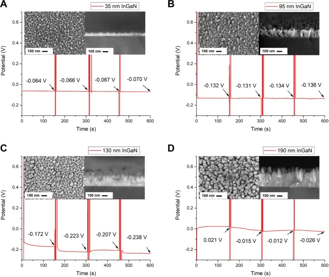
Figure 2 shows the OCP measurements as a function of time for the InN/InGaN samples where the InGaN layer thickness is varied for the fixed, best 0.8 ML InN coverage. The InGaN layer thickness is 35 (Fig. 2A), again 95 (Fig. 2B), 130 (Fig. 2C) and 190 nm (Fig. 2D). The InN/InGaN samples are alternately immersed for 150 seconds in 0.1 and 1 M KCl aqueous solutions. The insets show the corresponding top-view and cross-sectional SEM images. The columnar structure seen in cross-sectional SEM is observed for all samples with the undulated surface morphology visible in top-view SEM. The individual, isolated columns, seen in top-view SEM, grow in height and diameter and dominate with increasing layer thickness. They are almost invisible for the 35 nm thick InGaN layer. In the OCP measurements, the 0.8-ML-InN/35-nm-InGaN sample and the 0.8-ML-InN/95-nm-InGaN sample show comparable low response towards the KCl concentration with high stability. The thicker 130- and 190-nm-InGaN samples develop a clear response towards the KCl concentration and large drift. Because of the technological- and cost relevance of thin layers, we choose the 0.8-ML-InN/35-nm-InGaN sample to evaluate the low sensitivity for a wide KCl concentration range and the high long-time stability required for a reference electrode.
Figure 2.
Open circuit potential as function of InGaN layer thickness. OCP as a function of time for the InN/InGaN electrode and Ag/AgCl reference electrode immersed alternately for 150 seconds in 0.1 and 1 M KCl aqueous solutions. The insets show the top-view- (left-hand side) and cross-sectional (right-hand side) SEM images. The In0.45Ga0.55N layer thicknesses are (A) 35, (B) 95, (C) 130 and (D) 190 nm. The InN deposition amount is 0.8 ML for all samples.
OCP over a wide concentration range and long time
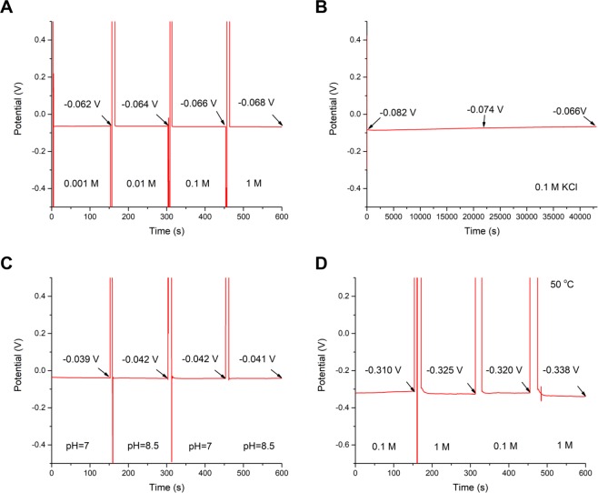
Figure 3A shows the OCP measurements as a function of time for the InN/InGaN sample with 0.8 ML InN coverage and 35 nm InGaN layer thickness successively immersed for 150 seconds in 0.001, 0.01, 0.1 and 1 M KCl aqueous solutions. Over the whole concentration range the potential response with drift is less than 10 mV, satisfying the demands on a reference electrode. Also the long-time OCP response, shown in Fig. 3B, qualifies the 0.8-ML-InN/35-nm-InGaN sample as a reference electrode with a low drift of less than 2 mV/hour over 12 hours in 0.1 M KCl aqueous solution.
Figure 3.
Open circuit potential for the InN/InGaN reference electrode. (A) OCP as a function of time for the 0.8-ML-InN/35-nm-In0.45Ga0.55N electrode and Ag/AgCl reference electrode successively immersed for 150 seconds in 0.001, 0.01, 0.1 and 1 M KCl aqueous solutions. (B) Long-time OCP measurement for the same sample over 12 hours in 0.1 M KCl aqueous solution. (C,D) OCP as a function of time for the 0.8-ML-InN/35-nm-In0.45Ga0.55N electrode and Ag/AgCl reference electrode immersed alternately for 150 seconds (C) in water and pH 8.5 KOH aqueous solutions and (D) in 0.1 and 1 M KCl aqueous solutions at 50 °C.
After having identified the best reference electrode tested in KCl aqueous solution we also cross-checked in KOH alkaline solution and at elevated temperature. In acidic solutions, the InN/InGaN electrodes inherently show no response to the positively charged hydrogen ions24. In Fig. 3C,D the corresponding measurements are shown for cycling alternately for 150 seconds between water and pH 8.5 KOH aqueous solution (Fig. 3C) and between 0.1 and 1 M KCl aqueous solutions at 50 °C (Fig. 3D). The reference electrode behaves equally well in KOH aqueous solutions. At 50 °C it is slightly less stable, but still acceptable. Corrosion is neither observed in alkaline nor in acidic solutions24.
Discussion
From the experimental results, two main conclusions follow: (i) there is an optimum InN coverage and (ii) there is an optimum surface morphology. As outlined, the basic idea is to create a surface with balanced surface charge distribution at the nanoscale. This clearly calls for a particular surface morphology covered with a particular amount of InN. We started to imagine a c-plane In0.45Ga0.55N layer having a planar surface, which is charge neutral. However, a charge neutral surface is not expected to produce a stable response. But any evolution of surface morphology will expose sidewalls with negative surface charge while sub-ML deposition of InN will add positive surface charge on top. Both together, rightly balanced, will give rise to the nanoscale regions with positive and negative surface charge for concentration insensitive and stable electrochemical response. The band structure of the InGaN/InN heterostructure has been drawn in ref.44 in the context of photoelectrochemical water splitting, including the pulling down of the surface band bending upon deposition of InN. This describes the attraction of electrons inside the InGaN layer to the surface due to the positive surface charge of InN. Figure 4 shows a graphics of the undulated InGaN surface originating from the columnar growth, partially covered with InN in form of ML-islands. Away from the optimum distribution will be samples with low response but large drift or high response and small or large drift, as observed experimentally. This is correlated with the KPFM measurements providing direct access to the changes of the surface charge.
Figure 4.
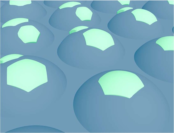
Spatial surface charge engineering. Graphics of the undulated InGaN surface with sub-ML InN coverage. The sidewalls are negatively charged and the InN ML-islands on top are positively charged.
Figure 5 shows a diagram of the relative surface potentials measured by KPFM of the electrodes as a function of the InN deposition amount and InGaN layer thickness. The KPFM resolution of 100 nm allows only average values. The nanoscale surface features are not captured in the relative surface potential. The KPFM measurements are performed under illumination to obtain a stable and reproducible signal. In the dark, random fast and slow charging and discharging processes at the surface turn the measurements unreliable45,46. Such processes are screened and stabilized under illumination. As a function of InN amount the surface potential continuously increases. This evidences the subsequent addition of positive surface charge with increasing amount of deposited InN. Also with increase of the InGaN layer thickness the surface potential and, hence, positive surface charge increases. This is attributed to the change of the surface morphology. With increasing InGaN layer thickness, the isolated columns exposing c-plane top facets develop. These c-plane top facets, covered with InN, add positive surface charge and reduce the negative surface charge associated with the undulated surface morphology, diminishing around the developing columns. Altogether, the red labeled samples with intermediate surface potentials are most concentration insensitive and stable in the OCP measurements. Also these samples are neighbors in a row as a function of the surface potential, no matter if the change is due to the InN amount or the InGaN layer thickness/surface morphology. For larger deviations of the surface potential the samples show significant response and/or drift. More than a correlation of structure, morphology, surface charge and electrochemical electrode properties is not possible at this stage, considering the highly complex nanoscale system. Nevertheless, our concept of spatial surface charge engineering is directly confirmed by this correlation, which successfully allowed to realize an InGaN-based all-solid-state reference electrode for electrochemical sensors.
Figure 5.
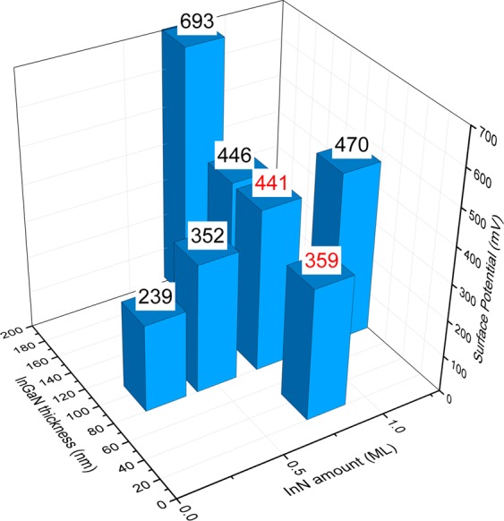
Correlation with surface potential. Diagram of the relative surface potentials measured by KPFM of the electrodes as a function of the InN deposition amount and InGaN layer thickness. Labeled in red are the best reference electrodes.
Conclusions
In conclusion, we have demonstrated a stable, epitaxial InN/InGaN-on-Si reference electrode for electrochemical sensors. A subtle interrelation of structure design, surface morphology and surface charge realized less than 10 mV/decade potential response in KCl aqueous solutions over a wide concentration range of 0.001 to 1 M and less than 2 mV/hour long-time drift in KCl aqueous solution with fixed concentration over 12 hours. This was made possible by our concept of spatial surface charge engineering, creating balanced nanoscale regions with positive and negative surface charge, such that a concentration insensitive and stable response originated. Paired with the InN/InGaN QD sensing electrode with solely changed structure and surface morphology, exhibiting super-Nernstian response, this opens the door to all-InGaN, all-solid-state, compact and robust electrochemical sensors with unprecedented performance.
Methods
Sample growth and characterization
Growth of the InN/InGaN structures was by plasma-assisted molecular beam epitaxy (PA-MBE) on p-type Si (111) substrates47,48. Active N was supplied by a radio-frequency (RF) plasma source. Prior to growth, the native oxide was removed from the Si surface by etching for 1 minute in 10% HF, the substrates were degassed for 30 min at 200 °C in the MBE load chamber and exposed to active N flux with 350 W RF power and 1.7 standard cubic centimeter per minute (sccm) N2 flow rate for 10 minutes at 800 °C in the MBE growth chamber. This surface nitridation results in improved crystal quality. Various growth temperatures and active N fluxes were adopted for InGaN and InN growth. For the two sets of samples explicitly discussed, the growth temperature was 510–520 °C for InGaN, close to the InGaN decomposition temperature, and the growth temperature for InN was 450 °C. The InGaN growth rate was 190 nm/hour, determined for compact, planar layers grown on GaN/sapphire substrates. The active N plasma source settings were 220–230 W and 1.2 sccm for an active N flux close to stoichiometric conditions. The InN deposition amount was between 0.25 and 1.2 monolayer (ML) and the InGaN layer thickness was between 35 and 190 nm, also referring to compact, planar layers on GaN/sapphire. The In content of the InGaN layer was 45%, determined by X-ray diffraction (XRD), shown in Supplementary Fig. S3. The surface morphology and cross-section were examined by top-view and cross-sectional scanning-electron microscopy (SEM). The relative surface potential was measured by Kelvin probe force microscopy (KPFM) using a Pt-Ir coated silicon tip. The spatial resolution was about 100 nm. Illumination was by a 3 W Hg discharge lamp. The original KPFM data are shown in Supplementary Fig. S4.
Electrode fabrication
For electrode fabrication, the samples were diced into about 1 × 1 cm2 pieces. Ga-In eutectic was deposited on the Si substrate back side for ohmic contact formation. This takes advantage of the ohmic contact formed between p-Si and In-rich n-InGaN49 and the high n-type conductivity of the InGaN layer due to defects acting as donors. Silver paste was distributed over the Ga-In eutectic and Si substrate back side for mounting the samples on Cu stripes. The samples and Cu stripes were wrapped with electrically insulating Teflon tape with a 0.031 cm2 hole on the sample front side. A scheme of the growth and electrode fabrication is shown in Fig. S5.
Open circuit potential measurements
The open circuit potential (OCP) was measured with the InN/InGaN electrodes and an Ag/AgCl reference electrode immersed in KCl aqueous solutions and connected to an electrochemical work station, see schematic drawing in Supplementary Fig. S6. As the Ag/AgCl electrode is a very good reference electrode, all measured potential changes are due to the InN/InGaN electrodes. For conditioning, the InN/InGaN electrodes were stored for three days in deionized water before the measurements. For sample selection, the InN/InGaN electrodes were alternately immersed for 150 seconds in 0.1 and 1 M KCl aqueous solutions. The most promising electrode was subjected to a wide KCl concentration range between 0.001 and 1 M and additionally tested for 12 hours in 0.1 M KCl aqueous solution to assess the long-time stability.
Supplementary information
Acknowledgements
This work was supported by: National Natural Science Foundation of China (No. U1501244, 51561135014), Guangdong Innovative Research Team Program (No. 2013C102), Program for Chang Jiang Scholars and Innovative Research Teams in Universities (No. IRT_17R40), Science and Technology Project of Shenzhen Municipal Science and Technology Innovation Committee (GQYCZZ20150721150406), Guangdong Provincial Key Laboratory of Optical Information Materials and Technology (Grant No. 2017B030301007), MOE International Laboratory for Optical Information Technologies and the 111 Project.
Author Contributions
L.Y.X., H.J.Y. and X.Y.W. performed the growth under supervision of P.W. L.Y.X. performed the measurements with support of Y.P.Q., L.J.R. and H.D.C. L.Y.X., P.W., G.F.Z. and R.N. discussed and interpreted the results. R.N. supervised the research and drafted the manuscript together with L.Y.X. All authors have discussed and commented on the manuscript.
Data Availability
The authors declare that the main data supporting the findings of this study are available within the paper and its Supplementary Information file. Other relevant data are available from the corresponding author upon reasonable request.
Competing Interests
The authors declare no competing interests.
Footnotes
Publisher’s note Springer Nature remains neutral with regard to jurisdictional claims in published maps and institutional affiliations.
Contributor Information
Guofu Zhou, Email: guofu.zhou@m.scnu.edu.cn.
Richard Nötzel, Email: richard.noetzel@scnu.edu.cn.
Supplementary information
Supplementary information accompanies this paper at 10.1038/s41598-019-51048-5.
References
- 1.Lewenstam A. Routines and challenges in clinical application of electrochemical ion sensors. Electroanal. 2014;26:1171–1181. doi: 10.1002/elan.201400061. [DOI] [Google Scholar]
- 2.Metkar SK, Girigoswami K. Diagnostic biosensors in medicine. Biocatalysis and Agricultural. Biotechnol. 2019;17:271–283. [Google Scholar]
- 3.Suzuki H. Microfabrication of chemical sensors and biosensors for environmental monitoring. Mater. Sci. Eng. C. 2000;12:55–61. doi: 10.1016/S0928-4931(00)00158-2. [DOI] [Google Scholar]
- 4.Ejeian F, et al. Biosensors for wastewater monitoring. Biosensors and Bioelectron. 2018;118:66–79. doi: 10.1016/j.bios.2018.07.019. [DOI] [PubMed] [Google Scholar]
- 5.Ye Y, Guo H, Sun X. Recent progress on cell-based biosensors for analysis of food safety and quality control. Biosensors and Bioelectron. 2019;126:389–404. doi: 10.1016/j.bios.2018.10.039. [DOI] [PubMed] [Google Scholar]
- 6.Brooks SL, Higgins IJ, Newman JD, Turner APF. Biosensors for process control. Enzyme and Microbial Technol. 1991;13:946–955. doi: 10.1016/0141-0229(91)90115-Q. [DOI] [PubMed] [Google Scholar]
- 7.Mehrotra PJ. Biosensors and their applications. Oral Biology and Craniofacial Res. 2016;6:153–159. doi: 10.1016/j.jobcr.2015.12.002. [DOI] [PMC free article] [PubMed] [Google Scholar]
- 8.Bollella P, Gorton L. Enzyme Based Amperometric Biosensors. Curr. Opin. Electrochem. 2018;10:157–173. doi: 10.1016/j.coelec.2018.06.003. [DOI] [Google Scholar]
- 9.Cuartero M, Crespo GA. All-solid-state potentiometric sensors: a new wave for in-situ aquatic research. Curr. Opin. Electrochem. 2018;10:98–106. doi: 10.1016/j.coelec.2018.04.004. [DOI] [Google Scholar]
- 10.Kaisti M. Detection principles of biological and chemical FET sensors. Biosensors and Bioelectron. 2017;98:437–448. doi: 10.1016/j.bios.2017.07.010. [DOI] [PubMed] [Google Scholar]
- 11.Nag A, Mitra A, Chandra S. Physical graphene and its sensor-based applications. Sensors and Actuators A. 2018;270:177–194. doi: 10.1016/j.sna.2017.12.028. [DOI] [Google Scholar]
- 12.Gupta S, Murthy CN, Ratna Prabha C. Recent advances in carbon nanotube based electrochemical biosensors. Int. J. Biological Macromolecules. 2018;108:687–703. doi: 10.1016/j.ijbiomac.2017.12.038. [DOI] [PubMed] [Google Scholar]
- 13.Cui Y, Wei Q, Park H, Lieber CM. Nanowire nanosensors for highly sensitive and selective detection of biological and chemical species. Science. 2001;293:1289–1292. doi: 10.1126/science.1062711. [DOI] [PubMed] [Google Scholar]
- 14.Zheng G, Patolsky F, Cui Y, Wang WU, Lieber CM. Multiplexed electrical detection of cancer markers with nanowire sensor arrays. Nat. Biotechnol. 2005;23:1294–1301. doi: 10.1038/nbt1138. [DOI] [PubMed] [Google Scholar]
- 15.Kasem KK, Jones S. Platinum as a reference electrode in electrochemical measurements. Platinum Metals Rev. 2008;52:100–106. doi: 10.1595/147106708X297855. [DOI] [Google Scholar]
- 16.Chen S, et al. Current instability for silicon nanowire field-effect sensors operating in electrolyte with platinum gate electrodes. Electrochem. Sol. State. Lett. 2011;14:J34–J37. doi: 10.1149/1.3584082. [DOI] [Google Scholar]
- 17.Tarasov A, et al. True reference nanosensor realized with silicon nanowires. Langmuir. 2012;28:9899–9905. doi: 10.1021/la301555r. [DOI] [PubMed] [Google Scholar]
- 18.Salm E, et al. Electrical detection of nucleic acid amplification using an on-chip quasi-reference electrode and a PVC REFET. Anal. Chem. 2014;86:6968–6975. doi: 10.1021/ac500897t. [DOI] [PMC free article] [PubMed] [Google Scholar]
- 19.Duarte-Guevara C, et al. On-chip metal/polypyrrole quasi-reference electrodes for robust ISFET operation. Analyst. 2015;140:3630–3641. doi: 10.1039/C5AN00085H. [DOI] [PubMed] [Google Scholar]
- 20.Lu H, Schaff J, Eastman LF. Surface chemical modification of InN for sensor applications. J. Appl. Phys. 2004;96:3577–3579. doi: 10.1063/1.1767608. [DOI] [Google Scholar]
- 21.Lu YS, Huang CC, Yeh JA, Chen CF, Gwo S. InN-based anion selective sensors in aqueous solutions. Appl. Phys. Lett. 2007;91:202109. doi: 10.1063/1.2814035. [DOI] [Google Scholar]
- 22.Sofikiti N, et al. Direct immobilization of enzymes in GaN and InN nanocolumns: the urease case study. Appl. Phys. Lett. 2009;95:113701. doi: 10.1063/1.3227888. [DOI] [Google Scholar]
- 23.Alvi NH, et al. Highly efficient potentiometric glucose biosensor based on functionalized InN quantum dots. Appl. Phys. Lett. 2012;101:153110. doi: 10.1063/1.4758701. [DOI] [Google Scholar]
- 24.Alvi NH, et al. Highly sensitive and fast anion-selective InN quantum dot electrochemical sensors. Appl. Phys. Express. 2013;6:115201. doi: 10.7567/APEX.6.115201. [DOI] [Google Scholar]
- 25.Alvi NH, et al. An InN/InGaN quantum dot electrochemical biosensor for clinical diagnosis. Sensors. 2013;13:13917–13927. doi: 10.3390/s131013917. [DOI] [PMC free article] [PubMed] [Google Scholar]
- 26.Nötzel R. InN/InGaN quantum dot electrochemical devices: new solutions for energy and health. Natl. Sci. Rev. 2017;4:184–195. [Google Scholar]
- 27.Mahoob I, Veal TD, McConville CF, Lu H, Schaff WJ. Intrinsic electron accumulation at clean InN surfaces. Phys. Rev. Lett. 2004;92:036804. doi: 10.1103/PhysRevLett.92.036804. [DOI] [PubMed] [Google Scholar]
- 28.Van de Walle CG, Segev D. Microscopic origins of surface states on nitride surfaces. J. Appl. Phys. 2007;101:081704. doi: 10.1063/1.2722731. [DOI] [Google Scholar]
- 29.Veal TD, Jefferson PH, Piper LFJ, McConville CF. Transition from electron accumulation to depletion at InGaN surfaces. Appl. Phys. Lett. 2006;89:202110. doi: 10.1063/1.2387976. [DOI] [Google Scholar]
- 30.Bailey LR, et al. Band bending at the surfaces of In-rich InGaN alloys. J. Appl. Phys. 2008;104:113716. doi: 10.1063/1.3033373. [DOI] [Google Scholar]
- 31.Zhou C, et al. The current and emerging applications of the III-nitrides. ECS J. Solid State Sci. Technol. 2017;6:Q149–Q156. doi: 10.1149/2.0101712jss. [DOI] [Google Scholar]
- 32.Yin H, et al. Electrocatalytic activity of InN/InGaN quantum dots. Electrochem. Commun. 2019;106:106514. doi: 10.1016/j.elecom.2019.106514. [DOI] [Google Scholar]
- 33.Alarawi A, et al. Enhanced photoelectrochemical hydrogen production efficiency of MoS2-Si heterojunction. Optics Express. 2019;27:A352–A363. doi: 10.1364/OE.27.00A352. [DOI] [PubMed] [Google Scholar]
- 34.Alarawi A, Ramalingam V, He. JH. Recent advances in emerging single atom confined two-dimensional materials for water splitting applications. Mat. Today Energy. 2019;11:1–23. doi: 10.1016/j.mtener.2018.10.014. [DOI] [Google Scholar]
- 35.Das S, et al. A leaf-inspired photon management scheme using optically tuned bilayer nanoparticles for ultra-thin and highly efficient photovoltaic devices. Nano Energy. 2019;58:47–56. doi: 10.1016/j.nanoen.2018.12.072. [DOI] [Google Scholar]
- 36.Le VQ, et al. Van der Waals heteroepitaxial AZO/NiO/AZO/muscovite (ANA/muscovite) transparent flexible memristor. Nano Energy. 2019;56:322–329. doi: 10.1016/j.nanoen.2018.10.042. [DOI] [Google Scholar]
- 37.Retamal JRD, Ho CH, Tsai KT, Ke JJ, He JH. Self-organized Al nanotip electrodes for achieving ultralow-power and error-free memory. IEEE Trans. Elect. Dev. 2019;66:938–943. doi: 10.1109/TED.2018.2888873. [DOI] [Google Scholar]
- 38.Ning Y, Zhang Z, Teng F, Fang X. Novel transparent and self-powered UV photodetector based on crossed ZnO nanofiber array homojunction. Small. 2018;14:754. doi: 10.1002/smll.201703754. [DOI] [PubMed] [Google Scholar]
- 39.Yang W, et al. High-performance silicon-compatible large-area UV-to-visible broadband photodetector based on integrated lattice-matched type II Se/n-Si heterojunctions. Nano Lett. 2018;18:4697–4703. doi: 10.1021/acs.nanolett.8b00988. [DOI] [PubMed] [Google Scholar]
- 40.Zhang Y, et al. Self-powered dual-color UV-green photodetectors based on SnO2 millimeter wire and microwires/CsPbBr3 particle heterojunctions. Phys. Chem. Lett. 2019;10:836–841. doi: 10.1021/acs.jpclett.9b00154. [DOI] [PubMed] [Google Scholar]
- 41.Tang SY, et al. Enhanced photocarrier generation with selectable wavelengths by M-decorated-CuInS2 nanocrystals (M = Au and Pt) synthesized in a single surfactant process on MoS2 bilayers. Small. 2019;15:1803529. doi: 10.1002/smll.201803529. [DOI] [PubMed] [Google Scholar]
- 42.Zhang Z, Ning Y, Fang X. From nanofibers to ordered ZnO/NiO heterojunction arrays for self-powered and transparent UV photodetectors. J. Mater. Chem. C. 2019;7:223–229. doi: 10.1039/C8TC05877F. [DOI] [Google Scholar]
- 43.Alamri AM, Leung S, Vaseem M, Shamim A, He JH. Fully injet-printed photodetector using a graphene/perovskite/graphene heterostructure. IEEE Trans. Electr. Dev. 2019;66:2657–2661. doi: 10.1109/TED.2019.2911715. [DOI] [Google Scholar]
- 44.Kumar P, et al. Quantum dot activated indium gallium nitride on silicon as photoanode for solar hydrogen generation. Commun. Chem. 2019;2:4. doi: 10.1038/s42004-018-0105-0. [DOI] [Google Scholar]
- 45.Melitz W, Shen J, Kummel AC, Lee S. Kelvin probe force microscopy and its application. Surf. Sci Rep. 2011;66:1–27. doi: 10.1016/j.surfrep.2010.10.001. [DOI] [Google Scholar]
- 46.Deeb MA, et al. Photo-assisted Kelvin probe force microscopy investigation of three dimensional GaN structures with various crystal facets, doping types, and wavelengths of illumination. J. Appl. Phys. 2017;122:085307. doi: 10.1063/1.5000137. [DOI] [Google Scholar]
- 47.Soto Rodriguez PED, et al. Stranski-Krastanov InN/InGaN quantum dots grown directly on Si(111) Appl. Phys. Lett. 2015;106:023105. doi: 10.1063/1.4905662. [DOI] [Google Scholar]
- 48.Aseev P, et al. Near-infrared emitting In-rich InGaN layers grown directly on Si: towards the whole composition range. Appl. Phys. Lett. 2015;106:072102. doi: 10.1063/1.4909515. [DOI] [Google Scholar]
- 49.Hsu L, Walukiewicz W. Modeling of InGaN/Si tandem solar cells. J. Appl. Phys. 2008;104:024507. doi: 10.1063/1.2952031. [DOI] [Google Scholar]
Associated Data
This section collects any data citations, data availability statements, or supplementary materials included in this article.
Supplementary Materials
Data Availability Statement
The authors declare that the main data supporting the findings of this study are available within the paper and its Supplementary Information file. Other relevant data are available from the corresponding author upon reasonable request.


