Abstract
Solid-state nanopores are an emerging biosensor for nucleic acid and protein characterization. For use in a clinical setting, solid-state nanopore sensing requires sample preparation and purification, fluid handling, a heating element, electrical noise insulators, and an electrical readout detector, all of which hamper its translation to a point-of-care diagnostic device. A stand-alone microfluidic-based nanopore device is described that combines a bioassay reaction/purification chamber with a solid-state nanopore sensor. The microfluidic device is composed of the high-temperature/solvent resistance Zeonex plastic, formed via micro-machining and heat bonding, enabling the use of both a heat regulator and a magnetic controller. Fluid control through the microfluidic channels and chambers is controlled via fluid port selector valves and allows up-to eight different solutions. Electrical noise measurements and DNA translocation experiments demonstrate the integrity of the device, with performance comparable to a conventional stand-alone nanopore setup. However, the microfluidic-nanopore setup is superior in terms of ease of use. To showcase the utility of the device, single molecule detection of a DNA PCR product, after magnetic bead DNA separation, is accomplished on chip.
Keywords: Nanopore, microfluidics, DNA purification
1. Introduction
Integrated diagnostic platforms that combine biosensors within automated microfluidic devices are revolutionizing the detection of nucleic acids and proteins. Microfluidic systems process and analyze complex liquid samples collected from patients, automate and miniaturize laboratory scale sample preparation methods, reduce required sample and reagent volumes, and simplify assay complexity by integrating multiple components (e.g., sample preparation, acquisition, and quantification) into a single design.[1]–[5] There is significant interest in incorporation of sensitive single molecule sensing modalities into microfluidic devices that directly detect the biopolymers as well as provide additional information on composition, structure, and/or conformation.
Single-molecule biosensing techniques employing optical, electrochemical, magnetic, microelectromechanical, or ion-sensitive field-effect transistor readouts are used to successfully detect a wide range of analytes including nucleic acids [6]–[10] and peptides.[11][12] Of these technologies, nanopore sensing whereby a biopolymer is threaded through a 2–50 nm pore, under an applied electrical bias, is an exciting single molecule sensing technique at the forefront.[13]–[17] For example, DNA sequencing using a protein nanopore integrated into a portable microfluidic device, by Oxford Nanopore Technologies, represents a prime example and success.[18] Advances in solid-state nanopores are enabling the direct detection of dilute biopolymers using label-free and amplification-free methods. Specifically, solid-state nanopores offer several advantages over protein nanopores including control over nanopore geometry (diameter and thickness), greater mechanical stability, longer operating lifetimes, enhanced durability, sites for surface chemical modification, and fabrication processes not requiring the use of biologics.[19]
A solid-state nanopore is typically a sub-100 nm diameter hole in an insulating thin membrane separated by two electrolyte filled chambers. The device is operated by applying a voltage potential between the two chambers, which induces a baseline ionic current that becomes partially blocked as a charged biopolymer electrophoretically travels through the nanopore towards the oppositely charged electrode. The duration, blockage level, and frequency of these translocation events provide information on the analyte’s length, charge, shape, and concentration. As such, nanopores are used to characterize nucleic acids,[20]–[28] to detect proteins,[29]–[32] and to identify epigenetic modifications.[33]–[35] While nanopore sensors are small, the support equipment needed to purify nucleic acid or protein samples, and perform a nanopore experiment (liquid chambers, amplifiers, voltage clamps, electrical isolator, etc.) are not. As such, there is significant activity in integrating solid-state nanopores with microfluidic devices to expand their utility, to simply the detection process, and to accelerate the translation of these biosensors from research laboratories to clinical diagnostic settings.
For example, Jain et al. utilized a microfluidic device made of polydimethylsiloxane (PDMS) microchannels integrated with an electron beam sculpturing nanopore, and successfully used the device to detect DNA translocation.[36] Tahvildari et al. described a PDMS microfluidic device incorporating solid-state nanopore arrays fabricated by controlled dielectric breakdown.[37] Yanagi et al. reported a microfluidic device consisting of an acrylic flow cell integrated with solid-state nanopore arrays for DNA translocation detection.[38] Recently, Godin and co-workers demonstrated the use of PDMS-based microvalves to control dielectric breakdown and biological sample access to the nanopore.[39] Roman et al. described the use of a 3D-printer to fabricate a PDMS based microfluidic device incorporating a solid-state nanopore.[40] These nanopore-microfluidic devices represent successes, however additional opportunities exit for further advancements in: 1) liquid handling – e.g., acidic, basic, alcohol solutions; 2) sample introduction – e.g., number of ports; 3) sample preparation - e.g., chemical or biochemical reactions performed at room or elevated temperatures; 4) analyte isolation – e.g., purification via magnetic beads; 5) analyte detection – e.g., integration of solid-state nanopore sensor; 6) adaptability to commercial scale fabrication; and, 7) overall integration and automation.
Herein we describe an integrated stand-alone solid-state nanopore microfluidic chip (Figure 1) which offers: 1) material robustness via fabrication from Zeonex thermoplastic; 2) a reaction chamber for bioassays at room temperature up to 75 °C; 3) an analyte isolation chamber compatible with magnetic bead purification methods; 4) a multi-port liquid handling system to deliver one to eight solutions; 5) embedded silver chloride electrodes to apply a voltage potential between the two sides of the nanopore; 6) a multilayered design enabling independent access to the cis and trans sides of the nanopore chip; and 7) high-throughput fabrication via thermoplastic prototyping method.[41] The microfluidic-nanopore setup is easy to use and one can analyze assay volumes as small as 10 μL. Electrical noise measurement and DNA translocation experiments demonstrate performance comparable to a conventional stand-alone nanopore setup. Finally, single molecule detection of the DNA product from a PCR amplification reaction, after magnetic bead DNA separation, is accomplished on chip.
Figure 1.
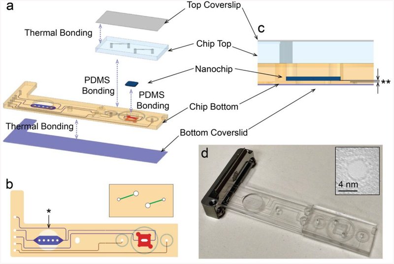
a) A schematic diagram of the microfluidic chip assembly. b) Top view design. The channels leading to/from the sample preparation chamber and to/from the bottom of the nanopore device are labeled blue, the channels leading to/from the top of the nanopore chamber are labeled in red. The blue and red channels are both cut into the bottom half of the two part device. The top half of the device is shown above and connects the four through hole channels fed by the red channels on the bottom of the device up through the Zeonex plastic to access the top of the nanopore chamber and the green channels. Both the red and blue channels flow past fluidically separated embedded electrodes. The bottom half of the device has the channels (red/blue) micro-machined on the bottom of the thick Zeonex plastic and sealed with a cover slip to form a channel while the top of this half has a feature micro-machined for the magnet holder (noted by asterisk). The top half is sealed with PDMS glue to the bottom half using the 3 micromachined tracks in the top of the bottom half as a guide. c) Zoom in cross section of the chip at the nanopore chambers. Noted that the chip bottom is machined from both top and bottom side, creating the thinnest layer of ~200 microns (labelled as **). d) A photograph of the microfluidic chip in its assembled state. Inset is the transmission electron micrograph of the nanopore taken after drilling.
2. Results and Discussion
2.1. Device assembly and NP integration.
An integrated microfluidic device containing a solid-state nanopore sensing module was designed, fabricated, and evaluated (Figure 1). While traditional microfluidic designs are typically 2D designs, the need to access both the top and bottom faces of a nanopore required a more complex multi-layer microfluidic design. The integrated nanopore-microfluidic device is composed of up-to five layers of silicon chip, plastics, and cover-slit sheets precisely aligned. The 3D microfluidic design is shown in Figure 1 with both the top (red) and bottom (blue) fluidic pathways highlighted. Each channel or pathway passes a fluidically isolated electrode at the entrance to either the cis (where the analyte is added) or trans side of the nanopore biosensor. Each half of the device consists of a 2 mm and 188 μm thick Zeonex Cyclo Olefin Polymer (COP) plastic bonded together to form fluidic channels based on micro-machined features in the 2 mm thick segment. Zeonex plastic was chosen for its optical and mechanical properties, including transparency, low auto-fluorescence, high glass transition temperature, solvent resistance, and machinability. It also features low moisture absorbance and biocompatibility with DNA and proteins.[42] An additional advantage of using a combined microfluidic-nanopore chip is it provides a closed system, thus preventing evaporation and air borne contamination while enabling the facile use of small working volumes.
In addition to two nanopore chambers formed on top and below the nanopore chips (shown in red in Figure 1a), the bottom chip contains a sample reaction/purification chamber for magnetic bead purification consisting of a 50 μL reaction volume below a micro-machined cavity designed to hold a magnet (shown in blue in Figure 1a). This chamber has its own outlet waste stream to introduce unprocessed sample and bypass the nanopore chamber. Upon completion of the purification protocol, the analyte of interest is released from the magnetic beads and flowed through the inlet channel to arrive at the nanopore sensing module of the device.
The nanopore was installed by sealing a nanopore chip within the bottom half of the device using a fast-curing PDMS sealant. Next, PDMS was used to seal the top half to the bottom half of the device using two circular tracks as a guide for PDMS application (Figure 1). This assembly process yielded fluidically isolated AgCl electrodes within the sensing module that are electrically connected only through the nanopore biosensor.
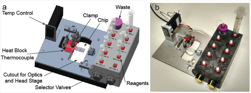
A custom build test instrument was designed to streamline the fluidic, temperature, and electronic control of the microfluidic device (Figure 2). The chip was interfaced to an 8-port assembly (while one port was used to connect to a waste container, only five ports were used to connect to the reaction solutions in the current experiments) with Dolomite connectors for easy “plug-and-play” access to the fluidic channels. The valves are external and located on the assembly not the chip. The five fluidic lines were then connected to a manual selector valve with nine Luer-Lok syringe connectors for an easy access. Based on the pathways chosen by the selector, any syringe can be used to access the device allowing for facile transitions between samples and buffers during an experiment. In addition to providing a chamber for magnetic bead capture, this same region of the chip was mechanically clamped to a temperature controller using an aluminum heat block, controlled by a programmable PID temperature controller. In order to minimize electromagnetic noise and to provide an easy interface between the microfluidic electrodes and the external electronics that operate the nanopore biosensor, electrical connections to the electrodes were made through a small terminal block, and the entire device was enclosed within a copper faraday cage.
Figure 2.
a) A schematic diagram of the custom designed test instrument with each component labeled. b) A photograph of the test instrument.
2.2. Verification of device’s fluid integrity.
The device integrity was first validated by assembling the device with a silicon chip not possessing a nanopore. A blue food dye solution was introduced into the assembled device, and we visually examined if the dye leaked between the two microfluidic pathways. No leakage between layers was observed (see SI). The AgCl electrodes were then inserted into the two chambers, and we measured the electrical signal. The measured current was below our detection limit in this setup confirming that the microfluidic chip was electrically isolated between the two chambers. To address the device integrity under high temperature, the microfluidic device was heated to 70 °C for an hour. Again, no dye leakage was observed and the electrical signal was isolation between the two chambers.
2.3. Device’s electrical integrity and noise analysis.
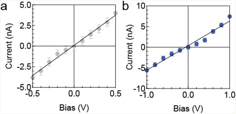
Next, we compared the electrical performance of a nanopore assembled in a conventional setup and the microfluidic setup. A nanopore was assembled into a conventional in-house setup made of Teflon.[43] Ionic current flow through the nanopore was measured as a function of incremental voltage ramp (Figure 3a). Linear regression analysis was used to obtain the pore’s conductivity of 7.31 ± 0.24 nS (R2 = 0.99); figure 3a). The diameter of the nanopore was calculated based on the equation;[13]
| (1) |
where Gopen is the conductivity during the open pore state, σ is the bulk conductivity, dpore is the diameter of the pore and l is the thickness of the membrane. The thickness of the membrane was pre-determined experimentally using ellipsometry to be 25 nm. From this equation, the pore’s diameter was calculated to be ~5.0 nm, and in agreement with the measurement obtained by electron microscopy obtained immediately after pore formation.
Figure 3.
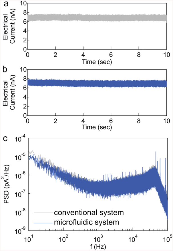
a) An open pore current trace of a 7 nm diameter nanopore (25 nm thickness) in a conventional chamber. The open pore current is 6.85 ± 0.18 nA. b) An open pore current trace of the same pore, but assembled into the microfluidic chamber. The open pore current is 6.96 ± 0.19 nA. Both traces were measured using a 100 KHz bandwidth. c) Comparison of the power spectral density of the current in the conventional system and microfluidic system. The electrolyte solution is 1 M KCl 50 mM phosphate 5 mM EDTA. +500 mV bias toward trans chamber. Signals were filtered using the Axon 200B built-in Bessel filter at 100 KHz.
Subsequently, the nanopore was removed from the conventional setup and assembled into the microfluidic setup. The open pore current conductivity was determined to be 5.95 ± 0.35 nS (R2 = 0.98), corresponding to a calculated pore diameter of ~4.5 nm. The slight decrease in open pore diameter is likely a result from disassembling and reassembling steps, as it involves drying the chip and a slight reduction in the pore’s wettability. In a separated experiment, we directly assembled a new pore into the microfluidic device. Its conductivity matched the theoretical calculation based on its geometries.
The electrical noise data collected in a conventional in-house nanopore system compared to the microfluidic system is shown in Figure 4. A +500 mV voltage was applied to thetrans chamber, and the open pore current was recorded at full bandwidth. The open pore current in a conventional setup had a root-mean-square noise of 185 pA (figure 4a) measured at 100 KHz. While in the microfluidic system using the same pore, the root-mean-square noise was 192 pA (figure 4b), and similar to the measurement obtained on the conventional nanopore setup.
Figure 4.
I-V curve of 4.5 nm pore (25 nm thickness) inside a) the standard Teflon insert, b) the microfluidic device. The error bars show the root-mean-square noise of the current. Both data set was obtained using the same pore.
Apart from the root-mean-square noise during the continuous readout, the spectral noise in the frequency domain is also critical for the nanopore measurement. To maximize the temporal resolution of our system, we used the full bandwidth of our amplifier (~100 kHz) and examined the noise in the system by performing power spectral density measurements. The microfluidic system consistently produced a current with low-1/f noise level, comparable with the conventional setup shown in figure 4c.
2.4. Model DNA translocations.
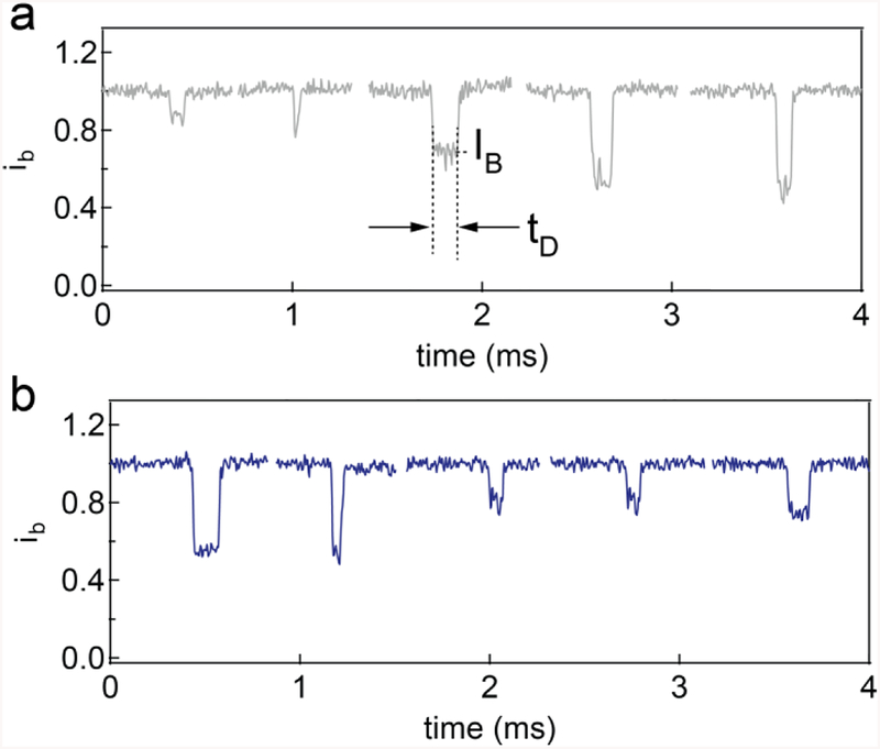
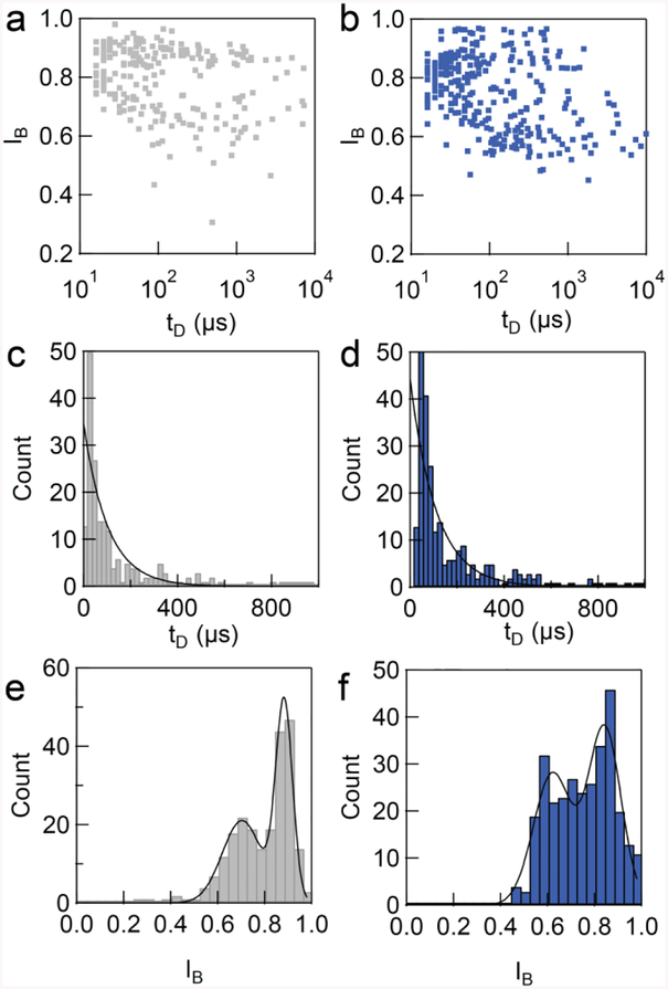
We performed DNA translocation experiments using a 5 kbps long DNA, as a model representative DNA sample to evaluate the performance of the chip. First, we performed DNA translocation through a nanopore assembled in the conventional setup with an applied bias of +500 mV to the trans chamber. The current versus time traces showed the characteristic events (Figure 5a). A couple hundred of events were collected (N = 231), and analyzed to create a scatter plot of the fractional blockage current (IB) and translocation dwell time (tD) (Figure 6a). The dwell time histogram was fit to an exponential decay function to give the characteristic translocation time of 103 ± 18 μs (Figure 6c). The event amplitude showed single level translocation clustering at 0.70 ± 0.20 and 0.88 ± 0.08, (Figure 6e) when fitted by a bimodal distribution. The expected blocked level of the DNA inside the pore was estimated using the equation;[24]
| (2) |
where dDNA is diameter of DNA (2.3 nm). Thus, the first event amplitude clustering at IB ~ 0.88 reflected collision events when the DNA attempted to enter the pore while the second population at IB ~ 0.70 corresponded to DNA successfully translocating through the pore.[24]
Figure 5.
Representative translocation events of a model 5 kbps NoLimits DNA collected with the nanopore in the conventional system a) or b) microfluidic system. Both dataset was obtained from the same experimental condition using the similar pore (4.2 nm diameter, 10 nm thickness).
Figure 6.
Analysis of the model 5 kbps DNA translocation events results in translocation dwell time (TD) and fractional current amplitude (IB). Each dot in the scatter pot represents the individual translocation event. a) The scatter plot of translocation events in regular insert, comparing with the translocation events in microfluidic system (b). c) The translocation time histogram inside a regular insert. The histogram was fit with exponential decay to yield the characteristic translocation time of 103 ± 18 μs (N = 231). d) The translocation dwell time of the events in microfluidic chip. Fitting results characteristic dwell time of 111 ± 21 μs (N = 304). The event amplitude histogram shows bimodal distribution which peaks are at 0.70 ± 0.20 and 0.88 ± 0.08 for conventional insert and 0.63 ± 0.20 and 0.86 ± 0.17 for microfluidic insert, respectively. The experiment was done in the same pore. For more experiment in different pores, see SI.
Once the experiment was completed, the nanopore was removed from the conventional setup insert and assembled into the microfluidic device, and the translocation experiment was performed again with the model 5 kbps DNA (Figure 6b). Analysis of the event amplitude and dwell time revealed that the translocation average event amplitude again contained two peaks at 0.70 ± 0.20 and 0.88 ± 0.08 (Figure 6f; N = 304) for the collision and translocation populations, respectively. This result was similar to that observed in the previous experiment. In both experiments, we observed a relatively large fraction of collisions versus full translocations (~60%) as expected given the small size of the nanopore. For example, Wanunu et al., reported ~50% collision using 4 nm pore with 4 kbps, and our data are consistent with that report.[24] The characteristic translocation time was determined to be 111 ± 21 μs, and comparable to the conventional setup.
To evaluate the performance of the nanopore in only the microfluidic device, we performed a subsequent DNA translocation experiment using a larger nanopore (10 nm diameter). Over the course of two hours we collected ~780 events (see SI). The event amplitude histogram shows a bimodal distribution at 0.97 ± 0.03 and 0.98 ± 0.01. The characteristic translocation time, when fitted to a double exponential decay function, was determined to be 39 ± 2 μs and 349 ± 56 μs.
2.5. Streamline DNA purification on a chip.
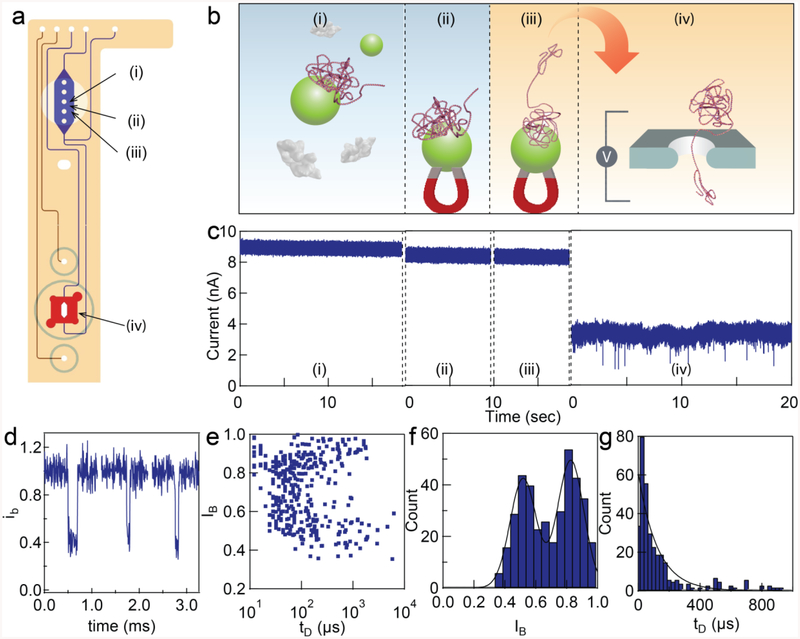
To demonstrate the utility of the microfluidic chip to purify a DNA sample from a crude PCR reaction prior to nanopore sensing, we performed the following experiment. After the PCR reaction was completed, 10 μL of the crude PCR solution was flowed into the microfluidic system at point a (Figure 7 chip diagram). The injection was halted once the solution reached the reaction/purification chamber. Next the silica-coated magnetic beads were injected into the chamber (the magnet was removed so that the DNA sample mixed and interacted with the magnetic beads freely in solution). The temperature of the chamber was increased to 70 °C for 10 minutes using the heating block, followed by cooling down to room temperature for another 10 minutes. The magnet was then placed on top of the chamber to collect the DNA-trapped magnetic beads while the remaining solution was washed from the chamber and removed via the outlet (Figure 7b). An additional rinsing step was performed with the wash solution. Finally the elution buffer, containing 10 mM Tris-EDTA buffer, was added to the reaction/purification chamber and the magnet was removed to allow the magnetic beads to disperse into the buffer solution. The microfluidic chip was then heated again to 50 °C for 2 minutes to facilitate the desorption of DNA from the magnetic beads (Figure 7c). Finally, the elution buffer containing DNA was flowed into the nanopore, and the translocation of the DNA through the nanopore was measured (Figure 7d). For additional information on this protocol and the corresponding fluidic path in the microfluidic chip, please see the SI. The event analysis revealed the characteristic translocation time of 125 ± 18 μs (N = 385) and event amplitudes of 0.51 ± 0.20 and 0.83 ± 0.20. Translocation of the 5 kbps NoLimits DNA in the same buffer condition yields similar amplitude and translocation time.
Figure 7.
On-chip PCR purification and nanopore sensing. a) diagram of a nanopore-microfluidic chip. b) A PCR amplicon was generated from lambda DNA template with KOD Hot Start Polymerese and the crude PCR solution was injected into the microfluidic chip for purification. (i) The DNA product from PCR reacted with the silica-coated magnetic nanoparticles inside the reaction chamber. (ii) The magnet is placed on top of the chip to pull down the DNA product. (iii) The beads were washed and released using elution buffer. (iv) The DNA product was sent to the nanopore for detection. c) Representative electrical current measured during each step (i-iv). d) Representative DNA translocation. The y-axis is a current normalized by the open pore current. e-g) Analysis of DNA event’s amplitude and dwell time. The statistics are shown in the main text. The experiment was done in the same pore (4 nm diameter, 5 nm thickness).
3. Conclusion
In summary, the fabrication and utilization of an integrated microfluidic-nanopore biosensor is described. This microfluidic-nanopore system exhibits comparable electrical noise to that observed in a conventional setup. DNA translocations are similar whether the solid-state nanopore is in the microfluidic device or the conventional setup. The microfluidic-nanopore biosensor possesses a reaction/purification chamber for performing bioassays and purifications at a controlled and defined temperature. Finally, separation of an analyte from the surrounding biological milieu is accomplished using magnetic beads. Thus, this method and the resulting biosensor are readily applicable to a number DNA and protein sensing applications. Studies are ongoing to refine the chip for simultaneous electrical and optical detection [23][44] via the nanopore. Our results highlight the advantages of combining thermoplastic microfluidic technologies with single molecule solid-state nanopore sensors, provide further impetus for new designs, and set the stage for implementation of such technologies into point-of-care applications.
4. Experimental Section
4.1. Microfluidic Chip.
The microfluidic chip composed of four Zeonex Cyclo Olefin Polymer (COP) layers (Zeon Chemicals, Louisville, KY) with two separable halves. Each half was a machined 2 mm thick Zeonex 690R plastic bonded to a 188 μm thick Zeonex ZF14 film. Features were micro-machined using a 3-axis Ultra Precision Milling Machine (Fraunhofer IPT, Aachen, Germany) using 150 μm by 1 mm end mills and a diamond fly cutting wheel. The fluidic channels were 200 μm square in cross section leading to a 40 μL nanopore chamber milled to insert/remove nanopore chips. Chambers for the nanopore were milled to created cavities to insert AgCl wire electrodes, designed to interface with either the top or bottom set of fluidic channels. The chip and cover slips on each half of the device were bonded using a solvent assisted thermal bonding method.[45] Both the chip and cover slip were immersed in decaline:ethanol 35:65 v/v% for 90 seconds and 30 seconds, respectively (decahydronaphthalene, mixture of cis+trans, Sigma-Aldrich, St. Louis, MO; denatured ethanol Sigma-Aldrich). Subsequently, the chip and coverslip were washed in an ethanol solution for two minutes and dried with compressed air. After the surface activation, the chip and cover slip were pressed together in a two-step process for sealing the channels in a hydraulic press. The conditions used for pre-bonding were 110 °C and 101 psi for 10 min, while the final bonding was conducted at 134 °C and 22 psi for 2 min.
4.2. Test Instrument Design.
A custom apparatus was designed to facilitate fluidic control, thermal regulation, and magnetic control. An aluminum heating block heated by an adhesive-backed silicon rubber heating pad (McMaster-Carr, Robbinsville, NJ) controlled by a programmable PID temperature controller (Fuji Electric, Japan) was incorporated under the microfluidic chip holder. Fluidic connections between the test instrument and the microfluidic chip were made through an eight-port connector (Dolomite, Norwell, MA) to connect the input and output of the top and bottom halves of the chip as well as a fifth connection to waste a container from the bottom segment. Nine Luer-Lok syringe attachments (IDEX Health & Science, Oak Harbor, WA) connected two manual selector valves (IDEX Health & Science, Oak Harbor, WA) and to 0.5 mm ID tubing (IDEX Health & Science, Oak Harbor, WA) were incorporated for interchangeable fluidic control between each syringe. Electrical connections to the electrodes were made through a small terminal block (WAGO, Germantown, WI), and electromagnetic noise was minimized by a removable copper faraday cage. A high-pull neodymium magnet (McMaster-Carr, Robbinsville, NJ) was manually placed into a machined cavity above the sample preparation chamber of the microfluidic chip to facilitate magnetic bead capture assays.
4.3. Nanopore Chip Fabrication and Electrical Measurement.
The nanopore chips were fabricated using an electron beam sculpturing technique.[46][47] Briefly, a <1 0 0> silicon wafer was coated with SiO2 (500 nm) and low-stress LPCVD silicon nitride film. The silicon wafer was etched through with KOH solution, creating a freestanding SiNx membrane with a thickness of ~20 nm. NPs were drilled on the SiNx membrane using a highly focused transmission electron microscope (JEOL 2010 FEG- TEM, Peabody, MA), to sputter the SiNx material away. A 4–6 nm pore was formed within 1 minute of focusing the beam. Prior to the experiment, the NP chips were treated with piranha solution (70% H2SO4: 30% H2O2) to remove potential organic contamination on the surface and enhance the hydrophilicity of the pore’s wall, rinsed with DI water for three times, and kept in water.
To assemble the NP onto the microfluidic chip, the microfluidic channels were primed by flowing isopropanol, ethanol, and water through the channels to wet the channels’ walls. The NP was placed onto the NP chamber and sealed using the fast-curing polydimethylsiloxane (PDMS) glue (Ecoflex 5, Smooth-On, Macungie, PA). Subsequently, the top half of the chip was assembled using PDMS glue.
Both channels were filled with a nanopore buffer containing 1 M KCl, 50 mM TRIS buffer, and 5 mM EDTA at pH 8.0 (all of them were purchased separately from Sigma-Aldrich, St. Louis, MO). All buffers were filtered using a 0.02-μm syringe filter (Whatman Anatop 10 syringe filter, Sigma-Aldrich St. Louis, MO) and degassed in vacuum right before each usage. All experiments were performed inside a dark Faraday cage at constant temperature (22.0 ± 0.5 °C). Two Ag wires were electroplated in 2 M KCl solution to form AgCl electrodes. The lifetime of the electrodes is ≈3 hours and represents a limitation in the system. The electrodes were inserted into the electrode cavities providing access to the top and bottom set of the fluidic channels and connected to an Axon 200B amplifier (Molecular Devices, Sunnyvale, CA) as previously described.[48] Signals were filtered using the Axon 200B built-in Bessel filter at 100 KHz. The current response of the same nanopore chip in a regular insert and in the microfluidic insert was determined, and the data fit to a single exponential function to determine the capacitance (figure S8). The capacitance was approximately 2X greater in the microfluidic device, and future designs will place the electrodes nearer the nanopore to reduce stray capacitance.
Custom LabVIEW software was used to detect the presence of the events due to analyte translocation. The starting point of the event occurred when the current dropped 0.25 nA below the average open pore current and the event end point was defined when the current recovered to the open pore current value. The voltage clamp mode was used for all experiments. Event classification was performed off-line using a custom LabVIEW code to identify the average fractional current blockage (IB = <ib>/<io>) and translocation dwell time (tD).
4.4. Model DNA translocations.
The DNA translocation experiments were performed by flowing a nanopore buffer containing 1 nM of 5 kbps NoLimits DNA (ThermoFisher Scientific, Waltham, MA) through the microfluidic chip. Specifically, the 10 mM Tris-EDTA buffer containing DNA was sent to the nanopore cis chamber with minimal to no dilution in volume. During sensing, the cis chamber contained 10mM Tris-EDTA and the trans chamber contained 1M KCl. The salt concentration in both nanopore chambers were not equal, resulting in microscale mixing near the pore’s vicinity. Such a salt gradient is sufficient to perform the experiment as previously described.[49]
4.5. DNA purification on-a-chip.
A polymerase chain reaction (PCR) was performed (off chip) to create the 5,099 base pairs product from lambda DNA. The experimental detail and figure showing the fluidic path can be found in the supplementary information. Subsequently, the DNA product was purified using a silica-coated magnetic bead-based extraction protocol (magJET DNA Plasmid purification kits, Thermo Fisher Scientific, Cambridge, MA). Silica-coated magnetic beads were chosen because they bind nucleic acids in a pH sensitive manner enabling the selective capture of DNA from a biological sample, and subsequent release of DNA upon changing the pH. Furthermore, the magnetic core facilitates DNA isolation and purification using the magnet in the microfluidic chip. Lastly, the reactions in this purification procedure are mild, and do not deteriorate or adversely affect the nanopore.
The purification process involves five overall steps: 1) placement of magnetic bead nanoparticles inside the bioassay reaction/purification chamber of the microfluidic device; 2) binding of the DNA product to the magnetic beads; 3) rinsing the sample to remove unwanted contaminants; 4) releasing the DNA from the beads; and, 5) transferring the purified DNA to the nanopore sensor. The specific details are as follows. First, the nanopore buffer solution containing 1 M KCl, 50 mM phosphate buffer and 5 mM EDTA at pH 8.0 was flowed into the nanopore chamber (shown in red in figure 1a) through the reaction/purification chamber (shown in blue in figure 1a). Next, the magnetic particle suspension solution (2 μL) was mixed with isopropanol (18 μL), and the mixture was introduced into the reaction/purification chamber while the magnet was placed on top of the chamber. The valves were configured so that the solution flowed directly to the outlet bypassing the nanopore chamber. Next, the crude PCR solution (10 μL) was mixed with the neutralization solution (40 μL), and transferred to the reaction/purification chamber. The injection was stopped once the solution mixture reached the chamber. The magnet was removed and the temperature controller was turned on to heat the reaction chamber to 50 °C for 10 min. After the chamber was cooled down to room temperature, the magnet was placed back and 50 μL of the rinsing buffer was flowed through the chamber. Finally, 10 μL of the TE buffer (10 mM Tris-Cl buffer, 1 mM EDTA, pH 8.0) was incubated with the beads at 50 °C for two minutes to elute the nucleotides from the beads. Finally, the outlet flow was directed to the nanopore chamber so that the elution buffer containing pure DNA product was sent to the nanopore chamber for electrical detection. The purification process required approximately 15 minutes.
Supplementary Material
Acknowledgment
This work was supported in part by the NIH R21 EB017377, NIH T32 EB006359 JH, NIH T32 EB006359 JH,[50] and the Center for Future Technologies in Cancer Care CFTCC NIH U54 EB015403 at Boston University). We would like to thank Tal Hilton for helpful discussions on noise and bandwidth. Finally, we thank Drs. Alexis Sauer-Budge, David Chargin, and Richard Guilanya at Fraunhofer CMI – Center for Manufacturing Innovation – for assistance with the fabrication of the microfluidic devices.
Footnotes
Supporting Information
The Supporting Information is available free of charge on the Wiley Online Library or form the author.
Contributor Information
Allison Squires, Department of Chemistry, Stanford University, Stanford, CA 94305, USA.
Amit Meller, Departments of Biomedical Engineering, Chemistry, and Medicine, Boston University, Boston MA, 02215, USA; Department of Biomedical Engineering, Technion – Israel Institute of Technology, Haifa 32000, ISRAEL.
Mark Grinstaff, Departments of Biomedical Engineering, Chemistry, and Medicine, Boston University, Boston MA, 02215, USA.
References
- [1].Herr AE, V Hatch A, Throckmorton DJ, Tran HM, Brennan JS, V Giannobile W, Singh AK, Proc. Natl. Acad. Sci. U. S. A 2007, 104, 5268. [DOI] [PMC free article] [PubMed] [Google Scholar]
- [2].Mahalanabis M, Al-Muayad H, Kulinski MD, Altman D, Klapperich CM, Lab Chip 2009, 9, 2811. [DOI] [PubMed] [Google Scholar]
- [3].Lin C-C, Tseng C-C, Chuang T-K, Lee D-S, Lee G-B, Analyst 2011, 136, 2669. [DOI] [PubMed] [Google Scholar]
- [4].Cao Q, Mahalanabis M, Chang J, Carey B, Hsieh C, Stanley A, Odell CA, Mitchell P, Feldman J, Pollock NR, Klapperich CM, PLoS One 2012, 7, e33176. [DOI] [PMC free article] [PubMed] [Google Scholar]
- [5].Koh A, Kang D, Xue Y, Lee S, Pielak RM, Kim J, Hwang T, Min S, Banks A, Bastien P, Manco MC, Wang L, Ammann KR, Jang K-I, Won P, Han S, Ghaffari R, Paik U, Slepian MJ, Balooch G, Huang Y, Rogers JA, Sci. Transl. Med 2016, 8, 366ra165. [DOI] [PMC free article] [PubMed] [Google Scholar]
- [6].Goral VN, Zaytseva NV, Baeumner AJ, Lab Chip 2006, 6, 414. [DOI] [PubMed] [Google Scholar]
- [7].Dubus S, Gravel J-F, Le Drogoff B, Nobert P, Veres T, Boudreau D, Anal. Chem 2006, 78, 4457. [DOI] [PubMed] [Google Scholar]
- [8].Kim Y, Kim KS, Kounovsky KL, Chang R, Jung GY, dePablo JJ, Jo K, Schwartz DC, Lab Chip 2011, 11, 1721. [DOI] [PMC free article] [PubMed] [Google Scholar]
- [9].Quail M, Smith ME, Coupland P, Otto TD, Harris SR, Connor TR, Bertoni A, Swerdlow HP, Gu Y, BMC Genomics 2012, 13, 341. [DOI] [PMC free article] [PubMed] [Google Scholar]
- [10].Wang Y, Gu L, AIMS Mater. Sci 2015, 2, 448. [DOI] [PMC free article] [PubMed] [Google Scholar]
- [11].Choi J-W, Oh KW, Thomas JH, Heineman WR, Halsall HB, Nevin JH, Helmicki AJ, Henderson HT, Ahn CH, Lab Chip 2002, 2, 27. [DOI] [PubMed] [Google Scholar]
- [12].Alvarez M, Lechuga LM, Analyst 2010, 135, 827. [DOI] [PubMed] [Google Scholar]
- [13].Hille B, Ion Channels of Excitable Membranes, Sinauer 2001. [Google Scholar]
- [14].Bell NAW, Thacker VV, Hernández-Ainsa S, Fuentes-Perez ME, Moreno-Herrero F, Liedl T, Keyser UF, Lab Chip 2013, 13, 1859. [DOI] [PubMed] [Google Scholar]
- [15].Wei R, Gatterdam V, Wieneke R, Tampé R, Rant U, Nat. Nanotechnol 2012, 7, 257. [DOI] [PubMed] [Google Scholar]
- [16].Miles BN, Ivanov AP, Wilson KA, Doğan F, Japrung D, Edel JB, Chem. Soc. Rev 2013, 42, 15. [DOI] [PubMed] [Google Scholar]
- [17].Dekker C, Nat. Nanotechnol 2007, 2, 209. [DOI] [PubMed] [Google Scholar]
- [18].Mikheyev AS, Tin MMY, Mol. Ecol. Resour 2014, 14, 1097. [DOI] [PubMed] [Google Scholar]
- [19].Wanunu M, Meller A, Nano Lett 2007, 7, 1580. [DOI] [PubMed] [Google Scholar]
- [20].Tabard-Cossa V, Trivedi D, Wiggin M, Jetha NN, Marziali A, Nanotechnology 2007, 18, 305505. [Google Scholar]
- [21].Zhao Q, Sigalov G, Dimitrov V, Dorvel B, Mirsaidov U, Sligar S, Aksimentiev A, Timp G, Nano Lett 2007, 7, 1680. [DOI] [PMC free article] [PubMed] [Google Scholar]
- [22].Peng H, Ling XS, Nanotechnology 2009, 20, 185101. [DOI] [PMC free article] [PubMed] [Google Scholar]
- [23].Ivankin A, Henley RY, Larkin J, Carson S, Toscano ML, Wanunu M, ACS Nano 2014, 8, 10774. [DOI] [PMC free article] [PubMed] [Google Scholar]
- [24].Wanunu M, Sutin J, McNally B, Chow A, Meller A, Biophys. J 2008, 95, 4716. [DOI] [PMC free article] [PubMed] [Google Scholar]
- [25].Kwok H, Briggs K, Tabard-Cossa V, PLoS One 2014, 9, e92880. [DOI] [PMC free article] [PubMed] [Google Scholar]
- [26].Singer A, Rapireddy S, Ly DH, Meller A, Nano Lett 2012, 12, 1722. [DOI] [PMC free article] [PubMed] [Google Scholar]
- [27].Feng J, Liu K, Bulushev RD, Khlybov S, Dumcenco D, Kis A, Radenovic A, Nat. Nanotechnol 2015, 10, 1070. [DOI] [PubMed] [Google Scholar]
- [28].Squires A, Atas E, Meller A, Sci. Rep 2015, 5, 11643. [DOI] [PMC free article] [PubMed] [Google Scholar]
- [29].Han A, Schürmann G, Mondin G, Bitterli RA, Hegelbach NG, de Rooij NF, Staufer U, Appl. Phys. Lett 2006, 88, 093901. [Google Scholar]
- [30].Yusko EC, Johnson JM, Majd S, Prangkio P, Rollings RC, Li J, Yang J, Mayer M, Nat. Nanotechnol 2011, 6, 253. [DOI] [PMC free article] [PubMed] [Google Scholar]
- [31].Larkin J, Henley RY, Muthukumar M, Rosenstein JK, Wanunu M, Biophysj 2014, 106, 696. [DOI] [PMC free article] [PubMed] [Google Scholar]
- [32].Varongchayakul N, Huttner D, Grinstaff MW, Meller A, Sci. Rep 2018, 8, 1017. [DOI] [PMC free article] [PubMed] [Google Scholar]
- [33].Ivankin A, Carson S, Kinney SRM, Wanunu M, J. Am. Chem. Soc 2013, 135, 15350. [DOI] [PMC free article] [PubMed] [Google Scholar]
- [34].Shim J, Humphreys GI, Venkatesan BM, Munz JM, Zou X, Sathe C, Schulten K, Kosari F, Nardulli AM, Vasmatzis G, Bashir R, Sci. Rep 2013, 3, 1389. [DOI] [PMC free article] [PubMed] [Google Scholar]
- [35].Gilboa T, Torfstein C, Juhasz M, Grunwald A, Ebenstein Y, Weinhold E, Meller A, ACS Nano 2016, 10, 8861. [DOI] [PubMed] [Google Scholar]
- [36].Jain T, Jose Guerrero RS, Aguilar CA, Karnik R, Anal. Chem 2013, 85, 3871. [DOI] [PMC free article] [PubMed] [Google Scholar]
- [37].Tahvildari R, Beamish E, Tabard-Cossa V, Godin M, Lab Chip 2015, 15, 1407. [DOI] [PubMed] [Google Scholar]
- [38].Yanagi I, Akahori R, Aoki M, Harada K, Takeda K, Lab Chip 2016, 16, 3340. [DOI] [PubMed] [Google Scholar]
- [39].Tahvildari R, Beamish E, Briggs K, Chagnon-Lessard S, Sohi AN, Han S, Watts B, Tabard-Cossa V, Godin M, Small 2017, 13. [DOI] [PubMed] [Google Scholar]
- [40].Roman J, Jarroux N, Patriarche G, Français O, Pelta J, Le Pioufle B, Bacri L, ACS Appl. Mater. Interfaces 2017, 9, 41634. [DOI] [PubMed] [Google Scholar]
- [41].Tsao CW, Micromachines 2016, 7, 225. [DOI] [PMC free article] [PubMed] [Google Scholar]
- [42].Jena RK, Yue CY, Biomicrofluidics 2012, 6, 12822. [DOI] [PMC free article] [PubMed] [Google Scholar]
- [43].Squires AH, Gilboa T, Torfstein C, Varongchayakul N, Meller A, 2017, 353. [DOI] [PubMed]
- [44].McNally B, Singer A, Yu Z, Sun Y, Weng Z, Meller A, Nano Lett 2010, 10, 2237. [DOI] [PMC free article] [PubMed] [Google Scholar]
- [45].Wallow TI, Morales AM, Simmons BA, Hunter MC, Krafcik KL, Domeier LA, Sickafoose SM, Patel KD, Gardea A, Lab Chip 2007, 7, 1825. [DOI] [PubMed] [Google Scholar]
- [46].Li J, Stein D, McMullan C, Branton D, Aziz MJ, Golovchenko JA, Nature 2001, 412, 166. [DOI] [PubMed] [Google Scholar]
- [47].Kim MJ, Wanunu M, Bell DC, Meller A, Adv. Mater 2006, 18, 3149. [Google Scholar]
- [48].Wanunu M, Meller A, in Single-Molecule Tech. A Lab. Man (Eds: Selvin PR, T. Ha), Springer, New York: 2008. [Google Scholar]
- [49].Wanunu M, Morrison W, Rabin Y, Grosberg AY, Meller A, Nat. Nanotechnol 2010, 5, 160. [DOI] [PMC free article] [PubMed] [Google Scholar]
- [50].Grinstaff MW, Kaplan HM, Kohn J, ACS Biomater. Sci. Eng 2017, acsbiomaterials.7b00268. [DOI] [PMC free article] [PubMed] [Google Scholar]
Associated Data
This section collects any data citations, data availability statements, or supplementary materials included in this article.


