Abstract
Multi-metallic alloy nanoparticles (NPs) can offer tunable or modifiable localized surface plasmon resonance (LSPR) properties depending upon their configurational and elemental alterations, which can be utilized in various applications, that is, in photon energy harvesting, optical sensing, biomedical imaging, photocatalysis, and spectroscopy. In this work, a systematic investigation on the morphological and LSPR properties of multi-metallic alloy NPs incorporating Ag, Au, Pd, and Pt is presented on c-plane sapphire (0001). The resulting NPs exhibit much enhanced and tunable LSPR bands in the UV–VIS wavelength as compared to the previously reported mono-metallic NPs based on the considerable improvement in size and shape of nanostructures along with the electronic heterogeneity. Solid-state dewetting of sputtered bilayers (Ag/Pt), tri-layers (Ag/Au/Pt), and quad-layers (Ag/Au/Pd/Pt) is employed to demonstrate a wide variety of configurations, sizes, densities, and elemental compositions of Pt, AgPt, AuPt, AgAuPt, AgAuPt, and AgAuPdPt NPs by the systematic control of annealing temperature and deposition schemes. The distinct morphology and elemental composition of surface nanostructures are obtained by means of surface diffusion, intermixing, and surface/interface energy minimization along with the applied thermal energy. In addition, the sublimation of Ag atoms from the alloy nanostructure matrix significantly influences the structural, elemental, and thus optical properties of NPs by reducing the average size and Ag percentage in the alloy NPs. Based on the specific size, shape, and elemental composition of NPs, the excitation of LSPR is correlated to the dipolar, quadrupolar, multi-polar, and higher order (HO) modes along with the finite difference time domain simulation of local electric-field. The LSPR intensity is generally stronger with a higher percentage of Ag atoms in the alloy NPs and gradually diminished by the sublimation loss. However, even the mono-metallic and alloy NPs without Ag exhibited significantly improved and dynamic nature of plasmonic bands in the UV and VIS wavelength.
1. Introduction
Metallic nanostructures can exhibit the localized surface plasmon resonance (LSPR) through the coherent electron oscillations induced by the photon incidence, which can lead to the strong light absorption, scattering, hot carrier generation, and so forth, at the surface of NPs.1−4 In recent years, the localized surface plasmon resonance (LSPR) of metallic nanoparticles (NPs) have been extensively exploited for the development of advanced device applications in various fields such as energy conversion,5 electronics,6 photonics,7 sensors,8 biomedical,9 and optical spectroscopy.10 As just one example, the plasmon-induced strong light scattering by Ag NPs embedded in the back reflector significantly improve the light trapping in a silicon solar cell.11 The LSPR properties can be tuned by controlling the structure, shape, and density of metallic NPs, which enables the efficient control of optical field enhancement or concentration in the desired wavelength regions.12−14
In addition, the combination of various metallic components in a single NP, namely multi-metallic alloy NP, can offer additional opportunities to tune the LSPR properties by the control of elemental composition along with their structural parameters.15−17 Multi-metallic alloy NPs can offer superior components because of their multi-functionality, wide tunability, and multiple plasmon bands arisen from the synergy of the elements utilized.18 To date, various noble mono-metallic NPs (Ag, Au, Pd, and Pt) have been synthesized and pursued for various plasmonic applications such as energy harvesting, water purification, sensing and detection, high-density data storage, and ultrasensitive spectroscopy.1,11,19,20 However, the detailed investigation on the fabrication of multi-metallic alloy NPs having various elements in a single NP geometry has not been demonstrated up to now, which could provide a general framework for understanding the nanoscale surface morphology, growth characteristics, optical behaviors, and perspectives on the potential applications.
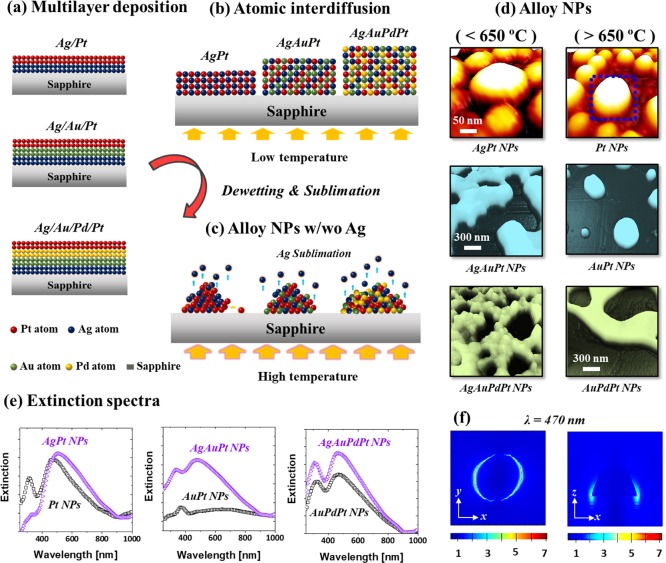
In this work, the detailed study and characterizations on the surface morphology and optical behavior of various mono-, bi-, tri-, and quad-metallic alloy NPs on sapphire (0001) are presented. The sputter-deposited Ag/Pt bilayers, Ag/Au/Pt tri-layers, and Ag/Au/Pd/Pt quad-layers are systematically annealed to induce the solid-state dewetting that yields nanostructures of various sizes, densities, configurations, and elemental compositions; the atomic diffusion, interdiffusion, alloying, nucleation, and energy minimization induce the growth of nanostructures, as illustrated in Figure 1. The optical properties of as-fabricated alloy NPs are assessed by UV–VIS–NIR spectra that show strong LSPR bands in the visible region and discussed in terms of various LSPR bands, that is, the dipolar (DR), quadrupolar (QR), multi-polar (MR), and higher order (HO) peaks, peak shift, and absorption band evolution. In addition, Ag atom sublimation significantly affects the surface morphology evolution as well as the LSPR properties of alloy nanostructures at above 650 °C, and the dynamic behaviors of LSPR bands such as intensity, position, and bandwidth are exploited based on the structure and elemental compositions of the alloy NPs.
Figure 1.
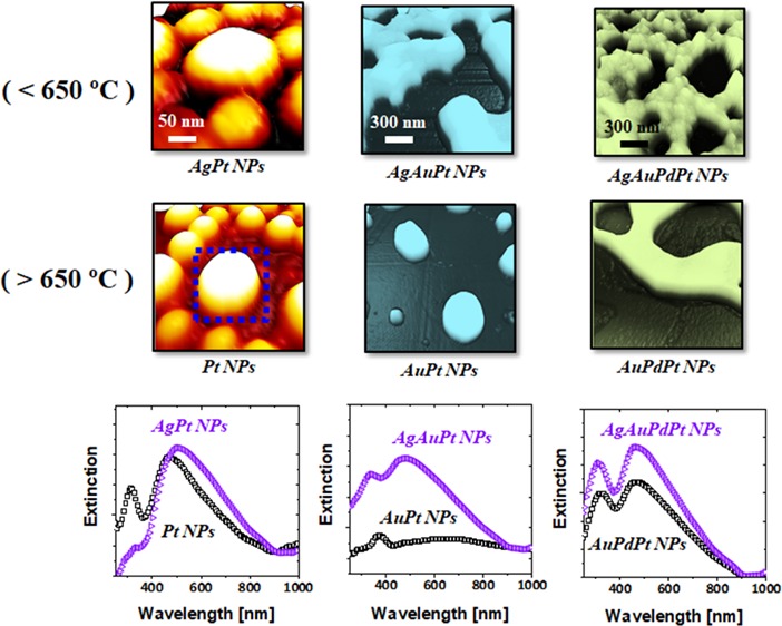
Fabrication of various mono- and multi-metallic nanoparticles (NPs) on sapphire (0001) based on the solid-state dewetting, interdiffusion, and Ag sublimation of multi-layer films. (a) Deposition schematics of Ag/Pt, Ag/Au/Pt, and Ag/Au/Pd/Pt multi-layers. (b) Atomic interdiffusion at low temperature. (c) Formation of alloy NPs along with Ag sublimation. (d) Typical mono- and multi-metallic NPs with and without Ag. (e) Comparison of extinction spectra of various NPs before and after Ag sublimation. (f) Localized e-field profile of the typical Pt NPs by finite difference time domain (FDTD) simulation.
2. Experimental Section
In this work, both-side polished 430 μm-thick c-plane sapphire (0001) was adapted as a substrate for the fabrication of various multi-metallic alloy NPs. Initially, a large piece of sapphire wafer was diced (0.6 × 0.6 mm2) using a mechanical saw. Then, the substrates were degassed in a pulsed laser deposition (PLD) chamber at 600 °C for 30 min under 1 × 10⁻⁴ Torr. After degassing, the substrates were ready for the deposition by the removal of trapped gaseous surface particulates and contaminants. Basic morphological and optical characterizations confirmed that the degassed sapphire had a smooth surface and was much cleaner, as shown in Figure S1a–c. Subsequently, various bi-, tri-, and quad-layers of Ag, Au, Pd, and Pt films were deposited on the cleaned sapphire (0001) substrates by using plasma-assisted sputtering, as shown in Figure 1a.
To fabricate various metallic alloy nanostructures, three different deposition schemes were adapted, as shown in Figure 1a, and the deposition sequence was chosen based on the diffusivity of the metal atoms such that the diffusivity decreases from the bottom to the top layer. The deposited sample was placed on a holder with an Inconel blank on backside and transferred to the PLD chamber for the nanostructure growth by annealing. Prior to the annealing, the chamber pressure was reduced below 1 × 10⁻⁴ Torr. The samples were annealed systematically at various target temperatures between 500 and 900 °C. The temperature was ramped at 4 °C/s and kept constant for 120 s at each target temperature. The annealing process was controlled by a computer program to maintain the consistency among samples. After reaching the final growth condition, the heating system was turned off, and samples were kept without breaking the vacuum inside the chamber until the system temperature was reduced to ambient over the course of time.
For the morphological characterizations, an atomic force microscope (AFM, XE-70, Park System, South Korea), scanning electron microscope (SEM, CX-200, COXEM, South Korea), and energy-dispersive X-ray spectroscope (EDS, Noran System 7, Thermo Fisher, USA) were adapted. The optical spectra of the multi-metallic alloy NPs were acquired by a NOST system (Nostoptiks, South Korea) equipped with light sources, optical microscope, various optical components, and CCD detector. To investigate the electric field (e-field) distributions of multi-metallic alloy NPs on sapphire, the simulations were performed using the finite difference time domain (FDTD) solutions (Lumerical, Canada). The dielectric constants of Au, Pd, and Pt were referred from the Palik models,21 and the Rakic constant was used for Ag.22 For the binary and ternary alloys, the dielectric constants were averaged from the pure Ag, Au, and Pt based on the atom % fraction.23,24 For more details, please refer the Supporting Information, Section S1.
3. Results and Discussion
Figure 1 shows the fabrication overview of mono- and multi-metallic alloy NPs on sapphire (0001) with the Ag/Pt, Ag/Au/Pt, and Ag/Au/Pd/Pt layers by the systematic annealing at various temperatures. Depending upon the annealing temperature and elemental configuration of multi-layer films, various configurations and sizes of AgPt and Pt NPs were achieved, which yield the distinct optical responses in the UV and VIS regions. The transformation of quasi-stable multi-layers can occur due to the solid-state dewetting (SSD) at the well-below melting point of elements in the films.25 When the thin film is deposited on a substrate at an ambient temperature, it generally can be metastable due to the insufficient diffusion. The surface diffusion can be activated by annealing at a sufficient temperature, which eventually induces the mass transport to reduce the energy at the surface and interface of film, giving rise to the evolution of isolated NPs.26,27 The surface morphology of resulting NPs directly depends upon the initial film thickness, diffusivity, and properties of the substrate. From the previous studies of Ag, Au, Pd, and Pt layers on sapphire, the Pd and Pt layers did not show any formation of definite NPs up to 600 °C due to their low surface diffusivity, while Au and Ag atoms dewetted well and formed the definite NPs even at ∼300 °C.28−31 In the case of bilayer or multi-layer films with various metal elements, the dewetting process can be additionally influenced by the interdiffusion, miscibility of the elements, surface energies, and interfacial energies between the substrate and various metal elements.32,33
In this work, the Ag layer was deposited first as displayed in Figure 1a for the different multi-layer configurations of films because of its higher surface diffusivity and lower interface energy with the sapphire than the other elements utilized. Also, it should be noted that the surface energy of Ag is much lower,34 and thus, the nucleation and growth of nanostructures can occur at a lower temperature with the sapphire/Ag/Pt configuration. Similarly, in the case of Ag/Au/Pt and Ag/Au/Pd/Pt multi-layer films, the atomic diffusivity decreases from the bottom to the top layer while the surface energy increased. Upon annealing, the metal atoms can start to intermix through the interfaces and consequently, the interface barrier can be fully consumed since Ag, Au, Pd, and Pt are miscible at nanoscale. Thus, the completely intermixed AgPt, AgAuPt, and AgAuPdPt alloys can be obtained, as shown in Figure 1b.35,36 With increasing temperature, the overall diffusion of atoms can be enhanced, and dewetting starts to occur at the alloy phase by void nucleation at low energy sites between the film and substrate.37 These pinholes/voids start to grow larger by edge retraction and coalescence with the neighboring ones, and the diffusing adatoms can start to accumulate, developing the interconnected nanoclusters. Finally, the interconnected nanoclusters can break into isolated islands due to the Rayleigh-like instability.32,38 In addition, the Ag atoms play another important role in the morphological and elemental evolution of NPs by sublimation due to its high vapor pressure.39 Ag atoms can begin to sublimate at 440 °C with the vapor pressure of 10–11 Torr, and the vapor pressure can reach 3 × 10⁻⁷ Torr only at 600 °C, which is nearly a 4 orders of magnitude increase. The rate of Ag sublimation accelerates with temperature, and thus, finally, the Ag component can be completely desorbed from the alloy NPs matrix resulting in the evolution of NPs without the Ag atoms, as illustrated in Figure 1c,d. Due to the concurrent effect of dewetting and Ag sublimation, the surface morphology of NPs along with the elemental composition transformed largely, as depicted by the typical example of three different alloy NPs in Figure 1d. This directly affects the LPSR intensity and peak position, as shown by the typical extinction spectra in Figure 1e. Furthermore, the definite and isolated NPs showed the strong e-filed enhancement at the edge of NPs based on the excitation of various plasmonic modes, as seen in Figure 1f.
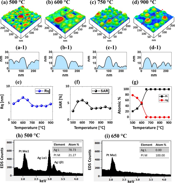
Figure 2 shows the detailed dewetting behavior of Ag7.5nm/Pt3.75nm bilayers between 500 and 900 °C. In specific, at 500 °C, the compact and irregular AgPt alloy NPs were formed, as shown in Figure 2a. Due to the complete intermixing and enhanced diffusion of atoms in the AgPt system, more definite AgPt NPs were obtained as compared to the pure Pt at this temperature.28 The average height (AH) and diameter (AD) of these AgPt NPs were around 50 and 20 nm, respectively, as extracted by the cross-sectional line profile, as shown in Figure 2a-1. The AgPt NPs gradually grew and became semispherical as the temperature increased up to 600 °C, as shown by AFM side views. The size and shape transformation of AgPt NPs in this temperature range can be correlated to the coalescence growth and surface energy minimization.32 Furthermore, the growth behavior of AgPt NPs are presented in terms of RMS roughness (Rq) and surface area ratio (SAR), as shown in Figure 2e,f respectively. Here, the Rq represents the average surface height fluctuations whereas the SAR represents the 3D surface area of the nanostructures. The Rq and SAR gradually increased from 4 to 10 nm and 5 to 8%, respectively, up to 600 °C along with the increased size of AgPt alloy NPs. However, although the enhanced dewetting can be expected with the increased temperature, the average size, Rq, and SAR of NPs sharply decreased between 650 and 750 °C. The size reduction of NPs can be due to the extensive sublimation of Ag atoms.
Figure 2.
Evolution of AgPt and Pt nanoparticles (NPs) on sapphire (0001) from the Ag7.5nm/Pt3.75nm bilayers annealed between 500 and 900 °C for 120 s. (a–d) Atomic force microscopy (AFM) side views of 250 × 250 nm2. (a-1–d-1) Cross-sectional line profiles of the NPs. (e, f) Summary plots of RMS roughness (Rq) and surface area ratio (SAR), respectively. (g) Summary of atom % of Ag and Pt. (h, i) Energy-dispersive X-ray spectroscopy (EDS) spectra of the AgPt and Pt NPs fabricated at 500 and 650 °C, respectively.
To confirm the sublimation of Ag and variation in the elemental composition, the elemental analysis was performed by EDS, as shown in Figure 2h,i and Figure S4. For all the samples, the EDS peaks of Al, O, and Pt were found to be consistent. However, the Ag peaks significantly decreased between 500 and 650 °C, suggesting the sublimation of Ag atoms from the alloy NP matrix.39 The overall atom % of Ag and Pt at a specific temperature are summarized in Figure 2g, which clearly showed that the atom % of Ag sharply decreased from 78.73 to 0% between 500 and 650 °C. At temperatures greater than 650 °C, the Ag atoms were completely sublimated, as observed in the EDS spectra and atom % plots. Therefore, the NPs obtained above 650 °C were pure Pt NPs. At 750 °C, the typical Pt NP had an average height and diameter of 25 and 50 nm, respectively. After increasing the temperature up to 900 °C, the average size of Pt NPs slightly increased, as shown in Figure 2d,d-1, which can be due to the coalescence growth of Pt NPs to gain the thermal stability with the low energy configuration.40 The corresponding Rq and SAR values were found to be somewhat similar, which can be due to the counterbalance between the minor size increase and density decrease along with diffusion. Meanwhile, it was also found that the uniformity and configuration of Pt NPs were improved at high temperatures. By comparing with the Pt NPs fabricated with the pure Pt film dewetting, significant improvement in terms of size, spacing, and uniformity was observed in this set.28
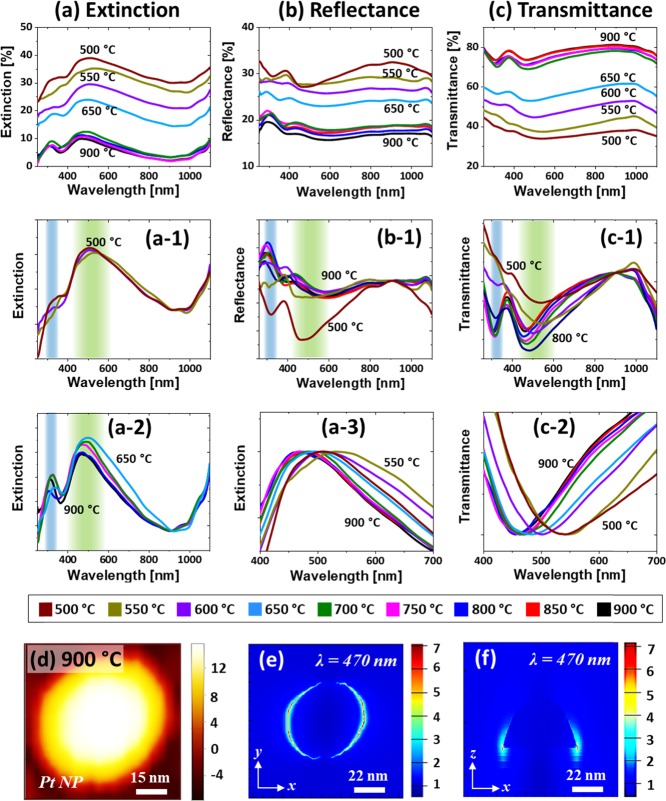
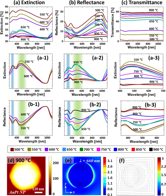
Figure 3 presents the LSPR properties of AgPt and Pt NPs fabricated with the Ag7.5nm/Pt3.75nm bilayers. The optical spectra demonstrated the wavelength-dependent characteristics along with the evolution of AgPt and Pt NPs at various temperatures. As shown in Figure 3a, the extinction spectra generally exhibited a strong and broad peak in the VIS region and a weak peak in the UV region for both AgPt and Pt NPs. In this set, the average size of AgPt alloy and Pt NPs was ∼20 nm in height and ∼50 nm diameter with the semispherical configurations, as discussed. Thus, the extinction peaks in the VIS and UV regions can be generated by the excitation of the dipolar (DR) and quadrupolar resonance (QR) modes of the small NPs.41,42 A detailed analysis of extinction spectra with the AgPt and Pt NPs was performed after the normalization, as shown in Figure 3a-1,a-2. The DR band of the AgPt NP did not show much variation between 500 and 600 °C although the NPs size increased, which can be due to the corresponding loss of Ag atoms along with the sublimation. Since the LSPR response is much stronger with Ag than Pt, the reduction of Ag component can correspondingly dampen the plasmonic intensity of the AgPt alloy NPs.42−44
Figure 3.
Optical properties of AgPt and Pt NPs fabricated with the Ag7.5nm/Pt3.75nm bilayers. (a–a-3) Extinction and normalized extinction spectra. (b, b-1) Reflectance and normalized reflectance spectra, respectively. (c–c-2) Transmittance and normalized transmittance spectra. (d) AFM image of the typical Pt NP selected for the finite difference time domain (FDTD) simulations. (e, f) E-field distributions of NPs in xy plane (top view) and xz plane (side view).
After the formation of Pt NPs above 650 °C, the DR was significantly reduced as shown in Figure 3a,a-2 due to the weaker LSPR response of Pt than AgPt NPs. It was also noted that the peak center gradually blue-shifted with the evolution of Pt NPs due to the size reduction. The overall blue shift of the DR peak from ∼505 to 460 nm was traced in Figure 3a-3. Furthermore, the peaks gradually narrowed as the Pt NP became more uniform at increased temperatures. For the detailed understanding on the plasmon resonance and localized e-field distribution, a typical semispherical Pt NP (AD, ∼50 nm and AH, ∼20 nm) was simulated, as shown in Figure 3d–f. The corresponding extinction spectra and e-field vector are provided in Figure S5, which showed the DR at ∼470 nm for the typical Pt NPs. From the simulation results, it was found that the e-field was strongly confined at the surface of NP, as seen in Figure 3e,f, but the higher order resonance peak was not observed. The resonance peak in the simulated extinction slightly varied (∼10 nm red shift) from the experimental one, which could be due to the size distribution of NPs in the real sample. Figure 3b,b-1 shows the corresponding reflectance spectra, which exhibit a minor dip in the UV region and a wide dip in the VIS region corresponding to the QR and DR bands, as discussed. Along with the sublimation of Ag, the VIS dip was gradually attenuated, as shown in Figure 3b-1, which can be correlated to the reduced absorption as well as the increased backscattering effect with the smaller size NPs. With the formation of Pt NPs, the reflectance dips were minorly attenuated due to the removal of the Ag component.41,42 In addition, the size reduction can also affect the dip intensity in the reflectance spectra. Similarly, the transmittance spectra in Figure 3c–c-2 exhibited a dip in the UV and VIS regions corresponding to the QR and DR modes with the AgPt and Pt NPs. The peak and dip gradually weakened along with Ag sublimation and size reduction, as discussed. The transmittance dips also clearly blue-shifted between ∼460 and 520 nm and narrowed as shown in Figure 3c-3 as the NP size was reduced and uniformity was improved.
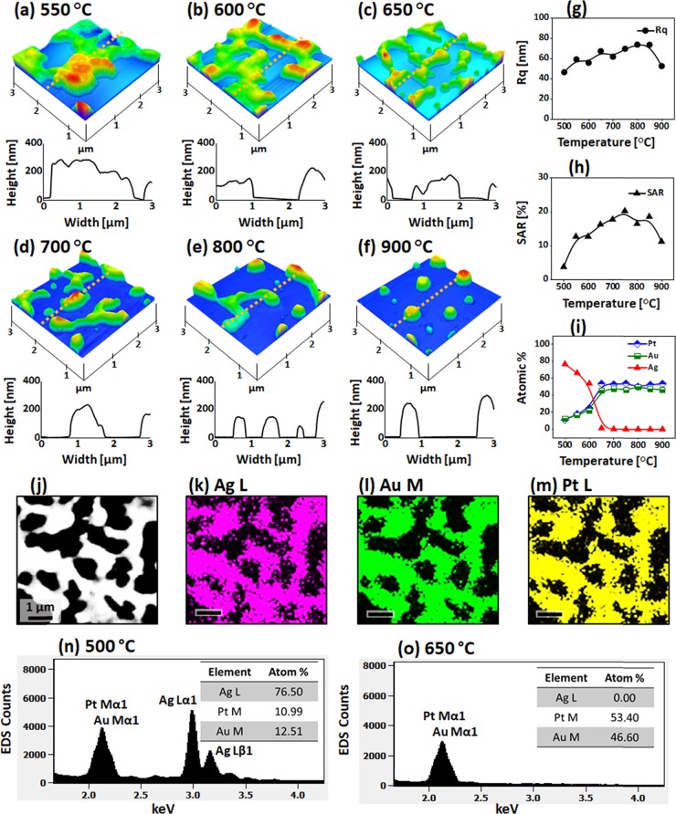
Figure 4 displays the fabrication of AgAuPt and AuPt alloy NPs with the Ag55nm/Au15nm/Pt15nm tri-layers annealed between 550 and 900 °C. The dewetting of Ag/Au/Pt tri-layers demonstrated various evolution stages such as void nucleation, void growth, interconnected nanoclusters, and isolated NP formation.40 The general dewetting behavior of the Ag/Au/Pt tri-layers was similar to that of the mono-metallic layer because of the miscible nature of Ag, Au, and Pt atoms at applied growth conditions.36,45 As discussed, the deposition sequence of tri-layers was adapted based on the decreasing diffusivity of metal atoms from the bottom to the top layer. Because of the high surface diffusivity, low surface, and interface energy of bottom layers, the overall atomic intermixing, diffusivity, and the dewetting process can be enhanced, as discussed. On the other hand, due to the increased layer thickness and different metallic interfaces, the interdiffusion process may also require additional thermal energy to completely intermix the tri-layers.46−48 Thus, the overall dewetting can be progressed at a slower phase with the tri-layers. For instance, the void nucleation and connected nanocluster growth occurred at 550 °C, as shown in Figure 4a, while the surface roughness only minorly evolved at lower temperatures. The void width was extended up to 2 μm, while the nanocluster height was ∼250 nm, as observed in the AFM 3D side views and cross-sectional line profiles. The large-scale AFM and SEM images of this set are provided in Figures S10 and S11. Along with the increased temperature, the voids grew further, resulting in the network-like nanoclusters, as seen in Figure 4b,c. Since the average height and surface area increased with the evolution of interconnected nanoclusters, the Rq and SAR also increased, as presented in Figure 4g,h.
Figure 4.
Large AgAuPt and AuPt alloy NPs on sapphire fabricated with the Ag55nm/Au15nm/Pt15nm tri-layers by annealing between 550 and 900 °C for 120 s. (a–f) AFM images of the alloy nanostructures. The corresponding line profiles are shown below the AFM images. (g–i) Summary plots of Rq, SAR, and atom % of Ag, Au, and Pt, respectively. (j–m) SEM image and corresponding elemental maps of Ag, Au, and Pt for the sample fabricated at 600 °C. (n, o) EDS spectra of the AgAuPt and AuPt alloy NPs at 500 and 650 °C, respectively.
The elemental analysis was performed for the sample annealed at 600 °C, as shown in Figure 4j–m. The SEM images and elemental maps of Ag, Au, and Pt matched each other well. This clearly indicates that Ag, Au, and Pt atoms were homogeneously intermixed in the alloy nanostructures. From the EDS spectra of AgAuPt alloy nanostructures at 500 °C, it can be observed that all Ag, Au, and Pt peaks were presented; however, at 650 °C, the Ag peaks completely vanished due to the sublimation. This again confirmed that the nanostructures were AgAuPt alloy up to 600 °C but were AuPt alloy above 650 °C. The corresponding variation of elemental compositions is summarized by the atom % plots in Figure 4i, which clearly showed a sharp decrement in the atom % of Ag between 500 and 600 °C. The surface morphology largely transformed above 650 °C as the interconnected nanoclusters showed the fluctuation in local width and started to break, as shown in Figure 4d. This evolution can be simultaneously affected by the Ag sublimation and Rayleigh-like instability.38 The Rq and SAR values slightly increased as the number of isolated structures increased despite the average size reduction. Between 700 and 900 °C, the interconnected AuPt nanoclusters were further fragmented and subsequently transformed toward spherical shape as seen in Figure 4e,f to reduce the overall energy of the surface and interface.49 This process can be ascribed to the tendency to reach the equilibrium shape. Once the fragmentation of large nanoclusters was finished, the isolated NPs tend to stabilize by merging with the neighboring ones, which results in the reduced areal density and relatively larger size of NPs. This was also shown by the decreasing trend of Rq and SAR.
Figure 5 shows the optical properties of AgAuPt and AuPt alloy NPs. Depending upon the variation of structures and elemental compositions, the LSPR properties were drastically varied from the previous set. As shown in Figure 5a, the extinction spectra demonstrated distinct spectral shape for the samples annealed below and above 600 °C. In specific, the partially dewetted AgAuPt nanoclusters (<600 °C) exhibited two peaks: one in the UV region and another in the VIS region, whereas the smaller AuPt NPs (>650 °C) showed weaker and broader UV and VIS peaks, as seen in Figure 5a-1,a-2. In general, the LSPR peaks were broader as compared to the small and isolated NPs in the previous set. Because of the large size of nanoclusters and NPs (above 1 μm), the extinction peaks in the UV and VIS wavelength can be assigned to the excitation of higher order resonance (HR) and multi-polar resonance (MR,) respectively.13 At increased temperatures, the LSPR peak intensity of AgAuPt NP gradually decreased, as shown in Figure 5a-1, which can be due to the Ag sublimation, as discussed. With the formation of the first connected and then isolated AuPt NPs at higher temperatures, the extinction spectra showed much wider and weaker peaks in the VIS region (420–580 nm), as shown in Figure 5a-2. Furthermore, the broadening effect of the VIS peaks along with the temperature is traced in Figure 5a-3. In contrast to the previous sets, this is an opposite behavior with the improved uniformity of the NPs. However, the broader LSPR response can be caused by the presence of Au component in the AuPt NPs due to the excitation of plasmon band at the longer VIS wavelength. The simulated e-field profile and the vector plot at the MR of a typical AuPt alloy NP are presented in Figure 5d–f, which showed the stronger intensity at the NP/sapphire interface due to the strong plasmonic confinement. In addition, the simulated extinction spectrum is presented in Figure S14, which exhibited two peaks corresponding to the HR and MR at 420 and 660 nm. These peak positions red-shifted with the stronger intensity as compared to the measured spectra, which can be due to the structural disparity in the simulated NP and real samples such as wide size and shape variation. The MR peak was found to be broader and much stronger likely due to the stronger resonance in the VIS region. Similarly, the reflectance spectra of AgAuPt and AuPt alloy nanoclusters are shown in Figure 5b,b-3, which generally exhibited two dips in the UV region at ∼450 nm and in the VIS region at ∼500 nm, corresponding to the HR and MR resonance, as discussed. The absorption dips of the AgAuPt alloy nanocluster were gradually attenuated and became broader with the sublimation of Ag atoms, as shown in Figure 5b-1.43,44 Furthermore, the evolution of AuPt nanocluster at increased temperatures caused the gradual flattening of the reflectance dips, as shown in Figure 5b-2,b-3, which can be due to the reduced absorption as the NP size was reduced. In the case of transmittance spectra, it did not exhibit obvious peaks or dip formation with the large AgAuPt and AgPt alloy nanoclusters, as shown in Figure 5c. Since the nanoclusters were generally large with more than 1 μm average diameter, the transmittance spectra can be strongly affected by the pronounced forward scattering.50 This can result in the flat transmittance even at the resonance wavelength.
Figure 5.
LSPR properties of the AgAuPt and AuPt alloy NPs fabricated with the Ag55nm/Au15nm/Pt15nm tri-layers. (a–a-3) Extinction and normalized extinction spectra. (b–b-3) Reflectance and normalized reflectance spectra. (c) Transmittance spectra. (d) AFM image of the typical AuPt NP. (e, f) E-field distribution and e-field vector plot of a typical AuPt NP, respectively.
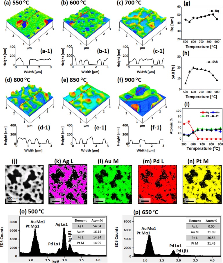
Figure 6 presents the evolution of AgAuPdPt and AuPdPt alloy nanoclusters from the Ag40nm/Au15nm/Pd15nm/Pt15nm quad-layers film by annealing between 550 and 900 °C for 120 s. The overall dewetting stages such as the hole initiation, hole growth, and interconnected nanoclusters were similar with the previous set. However, the dewetting extent was significantly altered, and thus, the resulting surface morphology of NPs was also drastically different at a specific temperature from the previous set. The quad-layers configuration of Ag/Au/Pd/Pt was adapted based on the diffusivity of metal as discussed. Since the Ag content decreased and the Pd layer was added at a constant total thickness, the dewetting process further slowed down because of the lower diffusivity of Pd atoms.32,34 Furthermore, with the increased number of various atomic layers and interfaces, the intermixing process can also be slowed down as well. However, the miscible nature of Ag, Au, Pd, and Pt atoms can induce similar dewetting stages as in the previous set. Along with the increased temperature, the intermixing between the atoms occurred at the interfaces of Ag/Au, Au/Pd, and Pd/Pt, and this can result in the completely alloyed layer, which starts to dewet by the void formation, as shown in Figure 6a. The void size varied between 500 and 1000 nm, as shown by the cross-sectional line profile in Figure 6a-1. At 550 °C, the size of voids was significantly small and less in number as compared to the previous set, which clearly indicates the low dewetting extent with the quad-layers configuration. The voids gradually increased by the coalescence of neighboring ones at 600 °C, as observed in Figure 6b. The corresponding large-scale AFM and SEM images are provided Figures S15 and S16.
Figure 6.
Evolution of large AgAuPdPt and AuPdPt alloy NPs from Ag40nm/Au15nm/Pd15nm/Pt15nm quad-layers by annealing between 550 and 900 °C for 120 s. (a–f) AFM side views of 3 × 3 μm2. (a-1–f-1) Cross-sectional line profiles. (g–i) Summary plots of Rq, SAR, and atom % of Ag, Au, Pd, and Pt, respectively. (j–n) SEM image and elemental maps of Ag, Au, Pd, and Pt for alloy nanoclusters fabricated at 600 °C, respectively. (o, p) EDS spectra of the AgAuPdPt and AuPdPt alloy NPs at 500 and 650 °C, respectively.
From the Rq and SAR plots in Figure 6g,h, they slightly increased along with the void growth between 500 and 600 °C. The detailed elemental characterization of AgAuPdPt alloy nanoclusters at 600 °C is presented in Figure 6j–n. The SEM images and elemental maps of Ag, Au, Pd, and Pt matched well, suggesting the homogeneous alloy formation in the nanoclusters. The detailed EDS map and line profiles are shown in Figure S18. In addition, the Ag sublimation was confirmed by the EDS spectra and summary of atom % plots in Figure 6i,o,p in which the Ag peaks and atom % sharply decreased between 500 and 600 °C. Above 650 °C, the atom % of Ag became zero, and the corresponding Ag peaks vanished, as observed in Figure 6p. Therefore, the nanoclusters obtained at above 650 °C only consisted of Au, Pd, and Pt. Since the Ag atoms were completely desorbed around 650 °C, the surface evolution of nanoclusters occurred somewhat mildly. As shown in Figure 6c–f, the connected nanoclusters gradually evolved with the increased spacing and branch width. However, the dewetting was not sufficient to generate isolated NPs up to 900 °C. Due to the formation of larger nanoclusters from the layered structures at increased temperatures, the Rq gradually increased. However, the SAR gradually decreased above 700 °C as the surface coverage was significantly reduced.
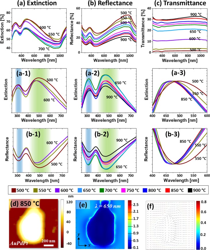
Figure 7 shows the optical properties of AgAuPdPt and AuPdPt alloy nanostructures fabricated with the Ag40nm/Au15nm/Pd15nm/Pt15nm quad-layers. As shown in Figure 7a, the extinction spectra generally exhibited two strong peaks in the UV and VIS regions with the large alloy nanoclusters. In the case of large nanoclusters, the UV and VIS extinction peaks can be assigned to the excitation of MR and HR, respectively, as discussed.13 As in the previous cases, the LSPR peaks were gradually attenuated and broadened along with the sublimation of Ag atoms, as shown in Figure 7a-1, indicating the dampening of the plasmonic effect. In contrast to the AgAuPt tri-alloy nanoclusters in the previous set, the AgAuPdPt quad-alloy nanoclusters showed the peak narrowing along with the dewetting of large voids. With the formation of AuPdPt nanocluster above 650 °C, the LSPR peaks further weakened and narrowed, as shown in Figure 7a-2. Furthermore, the MR in the VIS region showed a gradual blue shift at the increased temperature, as shown in Figure 7a-3, which can be due to the average size reduction of the alloy nanoclusters. From the FDTD simulation of typical AuPdPt alloy NP, it exhibited a relatively weaker e-field enhancement than previous sets, as shown in Figure 7d,e. Since the alloy NPs are generally large and irregular in shape, the e-field was distributed throughout the boundary of nanostructure, and the vector plot also showed multiple e-field directions, as observed in Figure 7e,f. The corresponding extinction spectrum of the typical AuPdPt alloy NP is shown in Figure S19, which exhibited two peaks at 390 and 650 nm. The peaks were much broader and tend to overlap likely due to the excitation of the multiple and higher order resonance bands. As compared to the previous set, the overall e-field intensity for high-temperature samples was weaker, which can be correlated to the addition of Pd while reducing Au and the wide coverage of NPs.
Figure 7.
Optical analysis of the AgAuPdPt and AuPdPt alloy nanostructures fabricated with the Ag40nm/Au15nm/Pd15nm/Pt15nm quad-layers. (a–a-3) Extinction and normalized extinction spectra. (b–b-3) Reflectance and normalized reflectance spectra. (c) Transmittance spectra. (d) AFM image of the typical AuPdPt NP. (e, f) Corresponding e-field distribution and vector plot of NP.
In addition, the reflectance spectra in Figure 7b also clearly show the formation of a narrow dip in the UV region and a wide dip in the VIS region. The reflectance dips correspond to the extinction peaks, which denotes the absorption bands due to the excitation of various LSPR, as discussed. The reflectance dip intensity gradually decreased with the evolution of voids and nanoclusters, as shown in Figure 7b-1, which can be correlated to the Ag sublimation as well as size reduction.43,44 The absorption dips were further reduced with the formation of AuPdPt alloy NPs at high temperatures, as shown in Figure 7b-2. It was also observed that the VIS dip gradually blue-shifted with the size reduction of nanoclusters, as shown in Figure 7b-3. In the case of transmittance spectra, as displayed in Figure 7c, it generally showed the flat response with both AgAuPdPt and AuPdPt alloy nanoclusters. Because of the large nanoclusters, the absorption dips in transmittance spectra may not be observed due to the strong forward scattering of large alloy nanoclusters, as discussed.13 However, a minor reduction of transmittance in the VIS region was realized for high-temperature samples, which can be due to the reduced forward scattering with the reduced size.
4. Conclusions
In summary, the various multi-metallic alloy nanostructures of novel metals (Ag, Au, Pd, and Pt) were demonstrated on c-plane sapphire (0001) along with their optical properties, which can be potential candidates in various plasmonic applications. In specific, Pt, AgPt, AgAuPt, and AgAuPdPt alloy NPs of various sizes, shapes, and densities were fabricated based on the self-assembly of sputtered metallic Ag/Pt bilayers, Ag/Au/Pt tri-layers, and Ag/Au/Pd/Pt quad-layers. The systematic annealing of various multi-layers led to the solid-state dewetting based on the enhanced diffusion, interdiffusion, and energy minimization mechanism. It was also observed that the mass driven self-assembly of the various multi-metallic alloyed nanostructures was accompanied by the sublimation of Ag atoms, which makes the growth behavior more dynamic as compared to the conventional SSD. In specific, the Ag atoms were extensively sublimated up to 650 °C along with the rapid dewetting of alloyed nanostructures, and thus, the NPs at higher temperatures did not consist of Ag. The overall dewetting of various metallic multi-layers was found to be similar to that of the mono-metallic film because of the enhanced miscibility of Ag, Au, Pd, and Pt atoms at nanoscale. However, the dewetting kinetics and hence the resulting nanostructures significantly varied from mono-metallic counterparts. These alloy nanostructures exhibited dynamic LSPR responses in the visible region and a minor resonance peak in the UV region. The size, shape, density, and elemental composition of the multi-metallic alloy NPs readily altered the LSPR properties. For instance, the VIS band generally blue-shifted with the size reduction whereas it was dampened with the reduced Ag percentage. Furthermore, the excitation of various plasmonic modes such as dipolar, quadrupolar, multi-polar, and higher order was observed with the various surface morphologies of the multi-metallic alloy nanostructures.
Acknowledgments
Financial support from the National Research Foundation of Korea (nos. NRF-2019R1A2C4069438 and NRF-2018R1A6A1A03025242) and in part by the research grant of Kwangwoon University in 2019 is gratefully acknowledged. Also, the work reported in this paper was conducted during the sabbatical year of Kwangwoon University in 2019.
Supporting Information Available
The Supporting Information is available free of charge on the ACS Publications website at DOI: 10.1021/acsomega.9b02066.
Additional morphological, elemental, and optical characterizations of multi-metallic alloy samples include the AFM images, EDS spectra, FDTD simulations, and optical spectra (PDF)
The authors declare no competing financial interest.
Supplementary Material
References
- Kuisma M.; Sakko A.; Rossi T. P.; Larsen A. H.; Enkovaara J.; Lehtovaara L.; Rantala T. T. Localized surface plasmon resonance in silver nanoparticles: Atomistic first-principles time-dependent density-functional theory calculations. Phys. Rev. B 2015, 91, 115431. 10.1103/PhysRevB.91.115431. [DOI] [Google Scholar]
- Shrivas K.; Shankar R; Dewangan K. Gold nanoparticles as a localized surface plasmon resonance based chemical sensor for on-site colorimetric detection of arsenic in water samples. Sens. Actuators, B 2015, 220, 1376–1383. 10.1016/j.snb.2015.07.058. [DOI] [Google Scholar]
- Unser S.; Bruzas I.; He J.; Sagle L. Localized surface plasmon resonance biosensing: current challenges and approaches. Sensors 2015, 15, 15684–15716. 10.3390/s150715684. [DOI] [PMC free article] [PubMed] [Google Scholar]
- Amendola V.; Pilot R.; Frasconi M.; Maragò O. M.; Iatì M. A. Surface plasmon resonance in gold nanoparticles: a review. J. Phys.: Condens. Matter 2017, 29, 203002. 10.1088/1361-648X/aa60f3. [DOI] [PubMed] [Google Scholar]
- Guo C. F.; Sun T.; Cao F.; Liu Q.; Ren Z. Metallic nanostructures for light trapping in energy-harvesting devices. Light: Sci. Appl. 2014, 3, e161 10.1038/lsa.2014.42. [DOI] [Google Scholar]
- Tsuboi A.; Nakamura K.; Kobayashi N. A Localized Surface Plasmon Resonance-Based Multicolor Electrochromic Device with Electrochemically Size-Controlled Silver Nanoparticles. Adv. Mater. 2013, 25, 3197–3201. 10.1002/adma.201205214. [DOI] [PubMed] [Google Scholar]
- Chen J.; Shi S; Su R.; Qi W.; Huang R.; Wang M.; Wang L.; He Z. Optimization and application of reflective LSPR optical fiber biosensors based on silver nanoparticles. Sensors 2015, 15, 12205–12217. 10.3390/s150612205. [DOI] [PMC free article] [PubMed] [Google Scholar]
- Wei H.; Abtahi S. M. H.; Vikesland P. J. Plasmonic colorimetric and SERS sensors for environmental analysis. Environ. Sci.: Nano 2015, 2, 120–135. 10.1039/C4EN00211C. [DOI] [Google Scholar]
- Dahlin A. B.; Tegenfeldt J. O.; Höök F. Improving the instrumental resolution of sensors based on localized surface plasmon resonance. Anal. Chem. 2006, 78, 4416–4423. 10.1021/ac0601967. [DOI] [PubMed] [Google Scholar]
- Yang B.; Lu N.; Qi D.; Ma R.; Wu Q.; Hao J.; Liu X.; et al. Tuning the intensity of metal-enhanced fluorescence by engineering silver nanoparticle arrays. Small 2010, 6, 1038–1043. 10.1002/smll.200902350. [DOI] [PubMed] [Google Scholar]
- Tan H.; Santbergen R.; Smets A. H. M.; Zeman M. Plasmonic light trapping in thin-film silicon solar cells with improved self-assembled silver nanoparticles. Nano Lett. 2012, 12, 4070–4076. 10.1021/nl301521z. [DOI] [PubMed] [Google Scholar]
- Yockell-Lelièvre H.; Lussier F.; Masson J.-F. Influence of the particle shape and density of self-assembled gold nanoparticle sensors on lspr and sers. J. Phys. Chem. C 2015, 119, 28577–28585. 10.1021/acs.jpcc.5b09570. [DOI] [Google Scholar]
- Kelly K. L.; Coronado E.; Zhao L. L.; Schatz G. C. The optical properties of metal nanoparticles: the influence of size, shape, and dielectric environment. J. Phys. Chem. B 2003, 668–677. 10.1021/jp026731y. [DOI] [Google Scholar]
- Zhang X.-Y.; Hu A.; Zhang T.; Lei W.; Xue X.-J.; Zhou Y.; Duley W. W. Self-assembly of large-scale and ultrathin silver nanoplate films with tunable plasmon resonance properties. ACS Nano 2011, 5, 9082–9092. 10.1021/nn203336m. [DOI] [PubMed] [Google Scholar]
- Gong C.; Dias M. R. S.; Wessler G. C.; Taillon J. A.; Salamanca-Riba L. G.; Leite M. S. Near-Field Optical Properties of Fully Alloyed Noble Metal Nanoparticles. Adv. Opt. Mater. 2017, 5, 1600568. 10.1002/adom.201600568. [DOI] [Google Scholar]
- Zhang H.; Wang C.; Li H.; Jiang L.; Men D.; Wang J.; Xiang J. Physical process-aided fabrication of periodic Au–M (M= Ag, Cu, Ag–Cu) alloyed nanoparticle arrays with tunable localized surface plasmon resonance and diffraction peaks. RSC Adv. 2018, 8, 9134–9140. 10.1039/C7RA13567J. [DOI] [PMC free article] [PubMed] [Google Scholar]
- Gao Y.; Jin F.; Su Z.; Zhao H.; Luo Y.; Chu B.; Li W. Cooperative plasmon enhanced organic solar cells with thermal coevaporated Au and Ag nanoparticles. Org. Electron. 2017, 48, 336–341. 10.1016/j.orgel.2017.06.003. [DOI] [Google Scholar]
- Nishi H.; Torimoto T.; Tatsuma T. Wavelength-and efficiency-tunable plasmon-induced charge separation by the use of Au–Ag alloy nanoparticles. Phys. Chem. Chem. Phys. 2015, 17, 4042–4046. 10.1039/C4CP04673K. [DOI] [PubMed] [Google Scholar]
- Li J.; Fang W.; Yu C.; Zhou W.; zhu L.; Xie Y. Ag-based semiconductor photocatalysts in environmental purification. Appl. Surf. Sci. 2015, 358, 46–56. 10.1016/j.apsusc.2015.07.139. [DOI] [Google Scholar]
- Mansuripur M.; Zakharian A. R.; Lesuffleur A.; Oh S.-H.; Jones R. J.; Lindquist N. C.; Im H.; Kobyakov A.; Moloney J. V. Plasmonic nano-structures for optical data storage. Opt. Express 2009, 17, 14001–14014. 10.1364/OE.17.014001. [DOI] [PubMed] [Google Scholar]
- Hieke S. W.; Breitbach B.; Dehm G.; Scheu C. Microstructural evolution and solid state dewetting of epitaxial Al thin films on sapphire (α-Al2O3). Acta Mater. 2017, 133, 356–366. 10.1016/j.actamat.2017.05.026. [DOI] [Google Scholar]
- Palik E. D.Handbook of Optical Constants of Solids III; Academic Press: New York, 1998. [Google Scholar]
- Kang M.; Ahn M.-S.; Lee Y.; Jeong K.-H. Bioplasmonic alloyed nanoislands using dewetting of bilayer thin films. ACS Appl. Mater. Interfaces 2017, 9, 37154–37159. 10.1021/acsami.7b10715. [DOI] [PubMed] [Google Scholar]
- Yang G.; Fu X.-J.; Sun J.-B.; Zhou J. Spectroscopic ellipsometry study on the optical dielectric properties of silver platinum alloy thin films. J. Alloys Compd. 2013, 551, 352–359. 10.1016/j.jallcom.2012.10.033. [DOI] [Google Scholar]
- Rakić A. D.; Djurišić A. B.; Elazar J. M.; Majewski M. L. Optical properties of metallic films for vertical-cavity optoelectronic devices. Appl. Opt. 1998, 37, 5271–5283. 10.1364/AO.37.005271. [DOI] [PubMed] [Google Scholar]
- Morawiec S.; Mendes M. J.; Priolo F.; Crupi I. Plasmonic nanostructures for light trapping in thin-film solar cells. Mater. Sci. Semicond. Process. 2019, 10. 10.1016/j.mssp.2018.04.035. [DOI] [Google Scholar]
- Rabkin E.; Amram D.; Alster E. Solid state dewetting and stress relaxation in a thin single crystalline Ni film on sapphire. Acta Mater. 2014, 74, 30–38. 10.1016/j.actamat.2014.04.020. [DOI] [Google Scholar]
- Sui M.; Li M.-Y.; Kunwar S.; Pandey P.; Zhang Q.; Lee J. Effects of annealing temperature and duration on the morphological and optical evolution of self-assembled Pt nanostructures on c-plane sapphire. PLoS One 2017, 12, e0177048 10.1371/journal.pone.0177048. [DOI] [PMC free article] [PubMed] [Google Scholar]
- Kunwar S.; Li M.-Y.; Pandey P.; Sui M.; Zhang Q.; Lee J. Evolution of morphological and optical properties of self-assembled Ag nanostructures onc-plane sapphire (0001) by the precise control of deposition amount. Mater. Res. Express 2016, 3, 125006. 10.1088/2053-1591/3/12/125006. [DOI] [Google Scholar]
- Pandey P.; Sui M.; Li M.-Y.; Zhang Q.; Kim E.-S.; Lee J. Shape transformation of self-assembled Au nanoparticles by the systematic control of deposition amount on sapphire (0001). RSC Adv. 2015, 5, 66212–66220. 10.1039/C5RA07631E. [DOI] [Google Scholar]
- Sui M.; Zhang Q.; Kunwar S.; Pandey P.; Li M.-Y.; Lee J. Study on the dimensional, configurational and optical evolution of palladium nanostructures on c-plane sapphire by the control of annealing temperature and duration. Appl. Surf. Sci. 2017, 416, 1–13. 10.1016/j.apsusc.2017.04.144. [DOI] [Google Scholar]
- Leroy F.; Borowik L̷.; Cheynis F.; Almadori Y.; Curiotto S.; Trautmann M.; Barbé J. C.; Müller P. How to control solid state dewetting: a short review. Surf. Sci. Rep. 2016, 71, 391–409. 10.1016/j.surfrep.2016.03.002. [DOI] [Google Scholar]
- Rahm J. M.; Erhart P. Understanding Chemical Ordering in Bimetallic Nanoparticles from Atomic-Scale Simulations: The Competition between Bulk, Surface, and Strain. J. Phys. Chem. C 2018, 122, 28439–28445. 10.1021/acs.jpcc.8b10874. [DOI] [Google Scholar]
- Zhang J.-M.; Ma F.; Xu K.-W. Calculation of the surface energy of FCC metals with modified embedded-atom method. Appl. Surf. Sci. 2004, 229, 34–42. 10.1016/j.apsusc.2003.09.050. [DOI] [Google Scholar]
- Esterina R.; Liu X. M.; Adeyeye A. O.; Ross C. A.; Choi W. K. Solid-state dewetting of magnetic binary multilayer thin films. J. Appl. Phys. 2015, 118, 144902. 10.1063/1.4932565. [DOI] [Google Scholar]
- Peng Z.; Yang H. Ag–Pt alloy nanoparticles with the compositions in the miscibility gap. J. Solid State Chem. 2008, 181, 1546–1551. 10.1016/j.jssc.2008.03.013. [DOI] [Google Scholar]
- Wang Y.; Jiang W.; Bao W.; Srolovitz D. J. Sharp interface model for solid-state dewetting problems with weakly anisotropic surface energies. Phys. Rev. B 2015, 91, 045303. 10.1103/PhysRevB.91.045303. [DOI] [Google Scholar]
- Jeong J.; Choi K.; Ye J. Investigation of a Rayleigh-Like Instability During the Solid-State Dewetting of Single-Crystal Nickel and Palladium Films. J. Korean Phys. Soc. 2018, 73, 90–94. 10.3938/jkps.73.90. [DOI] [Google Scholar]
- Asoro M. A.; Kovar D.; Ferreira P. J. In situ transmission electron microscopy observations of sublimation in silver nanoparticles. ACS Nano 2013, 7, 7844–7852. 10.1021/nn402771j. [DOI] [PubMed] [Google Scholar]
- Niekiel F.; Schweizer P.; Kraschewski S. M.; Butz B.; Spiecker E. The process of solid-state dewetting of Au thin films studied by in situ scanning transmission electron microscopy. Acta Mater. 2015, 90, 118–132. 10.1016/j.actamat.2015.01.072. [DOI] [Google Scholar]
- McPeak K. M.; Jayanti S. V.; Kress S. J. P.; Meyer S.; Iotti S.; Rossinelli A.; Norris D. J. Plasmonic films can easily be better: rules and recipes. ACS photonics 2015, 2, 326–333. 10.1021/ph5004237. [DOI] [PMC free article] [PubMed] [Google Scholar]
- Langhammer C.; Yuan Z.; Zorić I.; Kasemo B. Plasmonic properties of supported Pt and Pd nanostructures. Nano Lett. 2006, 6, 833–838. 10.1021/nl060219x. [DOI] [PubMed] [Google Scholar]
- Fleetham T.; Choi J.-Y.; Choi H. W.; Alford T.; Jeong D. S.; Lee T. S.; Lee W. S.; Lee K.-S.; Li J.; Kim I. Photocurrent enhancements of organic solar cells by altering dewetting of plasmonic Ag nanoparticles. Sci. Rep. 2015, 5, 14250. 10.1038/srep14250. [DOI] [PMC free article] [PubMed] [Google Scholar]
- Schmidl G.; Dellith J.; Schneidewind H.; Zopf D.; Stranik O.; Gawlik A.; Anders S.; et al. Formation and characterization of silver nanoparticles embedded in optical transparent materials for plasmonic sensor surfaces. Mater. Sci. Eng., B 2015, 193, 207–216. 10.1016/j.mseb.2014.12.001. [DOI] [Google Scholar]
- Manuela Müller C.; Spolenak R. Dewetting of Au and AuPt alloy films: a dewetting zone model. J. Appl. Phys. 2013, 113, 094301. 10.1063/1.4794028. [DOI] [Google Scholar]
- Krishna H.; Sachan R.; Strader J.; Favazza C.; Khenner M.; Kalyanaraman R. Thickness-dependent spontaneous dewetting morphology of ultrathin Ag films. Nanotechnology 2010, 21, 155601. 10.1088/0957-4484/21/15/155601. [DOI] [PubMed] [Google Scholar]
- Chng T. T.; Polavarapu L.; Xu Q.-H.; Ji W.; Zeng H. C. Rapid Synthesis of Highly Monodisperse AuxAg1–x Alloy Nanoparticles via a Half-Seeding Approach. Langmuir 2011, 27, 5633–5643. 10.1021/la2005216. [DOI] [PubMed] [Google Scholar]
- Kunwar S.; Pandey P.; Sui M.; Bastola S.; Lee J. Fabrication of Ternary AgPdAu Alloy Nanoparticles on c-Plane Sapphire by the Systematical Control of Film Thickness and Deposition Sequence. Metall. Mater. Trans. A 2018, 49, 2352–2362. 10.1007/s11661-018-4573-8. [DOI] [Google Scholar]
- Tao A. R.; Habas S.; Yang P. Shape control of colloidal metal nanocrystals. Small 2008, 4, 310–325. 10.1002/smll.200701295. [DOI] [Google Scholar]
- Liu S.; Chen G.; Prasad P. N.; Swihart M. T. Synthesis of monodisperse Au, Ag, and Au–Ag alloy nanoparticles with tunable size and surface plasmon resonance frequency. Chem. Mater. 2011, 23, 4098–4101. 10.1021/cm201343k. [DOI] [Google Scholar]
Associated Data
This section collects any data citations, data availability statements, or supplementary materials included in this article.


