Significance
We demonstrate, with simulations corroborated by experiments, that broadband long-wave infrared (LWIR) imaging is possible with a single flat lens with a thickness of 10 μm and a weight that is over 100 times less than conventional refractive optics. Reducing the weight and thickness of LWIR optics is crucial for increasing the range of camera-carrying drones as well as for reducing head and neck injuries among camera-borne soldiers. The technology discussed herein will be extremely useful not only to optics specialists but also to camera designers and users in general.
Keywords: diffractive lenses, chromatic aberrations, infrared imaging
Abstract
We experimentally demonstrate imaging in the long-wave infrared (LWIR) spectral band (8 μm to 12 μm) using a single polymer flat lens based upon multilevel diffractive optics. The device thickness is only 10 μm, and chromatic aberrations are corrected over the entire LWIR band with one surface. Due to the drastic reduction in device thickness, we are able to utilize polymers with absorption in the LWIR, allowing for inexpensive manufacturing via imprint lithography. The weight of our lens is less than 100 times those of comparable refractive lenses. We fabricated and characterized 2 different flat lenses. Even with about 25% absorption losses, experiments show that our flat polymer lenses obtain good imaging with field of view of 35° and angular resolution less than 0.013°. The flat lenses were characterized with 2 different commercial LWIR image sensors. Finally, we show that, by using lossless, higher-refractive-index materials like silicon, focusing efficiencies in excess of 70% can be achieved over the entire LWIR band. Our results firmly establish the potential for lightweight, ultrathin, broadband lenses for high-quality imaging in the LWIR band.
Long-wave infrared (LWIR) imaging refers to imaging in the wavelength band approximately from 8 m to 12 m, and is important for applications ranging from defense (1, 2), medicine (3), and agriculture (4) to environmental monitoring (3, 5). In order to attain high transparency, conventional refractive lenses in the LWIR band require materials such as silicon, germanium, or chalcogenide glasses. The weight of these conventional lenses can be too high for many applications. The increased weight limits the range of operation of unmanned aerial vehicles (6). In addition, such optics render head-mounted night vision goggles heavy, and cause neck and head injuries in soldiers as well as reducing their situational awareness (7). Here, we show that, by appropriately designing thin Multilevel Diffractive Lenses (MDLs), we can correct for image aberrations, including chromatic aberrations in the LWIR band, and thereby reduce the weight of such lenses by over 2 orders of magnitude when compared to conventional refractive lenses. In addition, since our MDLs are very thin, that is, thickness of , the design wavelength, and the resulting absorption losses are low, we can utilize polymers for the lens material, which are easier to manufacture (for instance, via microimprint lithography).
Conventional refractive optics is comprised of curved surfaces and become thicker with increasing resolution. That is, in order to bend light at larger angles, the radius of curvature must be lowered, and, consequently, the lens becomes thicker and heavier. Recently, metalenses have been proposed as a means to reduce the thickness of refractive lenses (8–11). Metalenses are comprised of constituent units that act as scattering elements (of subwavelength thickness), which render a prescribed local phase shift to light upon scattering. By engineering the spatial distribution of such constituent units in the lens plane, it is possible to correct for image aberrations. Although most demonstrations of metalenses have been in the visible and in the near-IR bands, there was a recent example of a metalens for one wavelength in the LWIR band, = 10.6 m (11). The constituent element of this metalens consisted of a square lattice of cylindrical pillars, whose diameter ranged from 1.5 m to 2.5 m, height = 6.8 m, and minimum pitch = 6.2 m. This device demonstrated a focusing efficiency of only 35% at the design wavelength. Another recent demonstration of a metalens-based LWIR microlens also achieved similar performance with similar fabrication challenges (12). No broadband LWIR metalenses have been demonstrated so far.
Recently, we showed that, when appropriately designed, MDLs could perform better than metalenses, while being easier to fabricate (13). Such MDLs have been demonstrated in the terahertz (14, 15) and in the visible bands (16, 17). By combining 2 MDLs, optical zoom has also been demonstrated (18). In fact, the MDLs require minimum feature width determined approximately by min/(2*NA), where min {} is the smallest wavelength in the operating spectral band and NA is the numerical aperture of the lens. This feature width is far larger than the corresponding value in the case of metalenses (which tend to be smaller than min/5). In addition, MDLs are naturally polarization-insensitive and can achieve high efficiencies over large bandwidths and at high NAs (13). The main drawback of MDLs is their somewhat complex multilevel geometry. However, with modern imprint lithography, such geometries can be manufactured at high volumes and at low costs (19). Here, we designed several MDLs for the LWIR, fabricated 2 of them, and then experimentally demonstrated the imaging performance using 2 different commercially available LWIR image sensors. It is important to distinguish our work from previous reports that utilize Fresnel lenses in the LWIR. An 80-m-thick polymer Fresnel lens combined with a 755-m-thick refractive silicon lens was used to report the thinnest LWIR lens (total device thickness 0.8 mm) capable of imaging (20). A high-order Silicon Fresnel lens made out of silicon was used in combination with an aperture for wide-angle imaging in the LWIR band as well (21), which had a total device thickness of 1 mm. In comparison, the device thickness of our single MDL is only 10 m (a reduction of 100) and it comprises a patterned polymer. Most importantly, MDLs are corrected for the entire operating bandwidth, while Fresnel lenses are not.
Results and Discussions
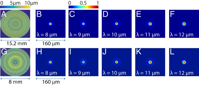
First, we designed rotationally symmetric MDLs, whose constituent element is a ring of width equal to 8 m, and whose height is determined by nonlinear optimization. This optimization is based upon a gradient-descent-assisted direct binary search (DBS) technique, a modified version of the conventional direct binary search method. Full details of our algorithm are published in refs. 14 and 15. Advanced methods like, for example, the adjoint method (22–26) can also be employed to achieve similar results with computational complexity comparable to our modified DBS technique. However, our method lends itself to a simple and modular implementation that enables incorporation of multiobjective functions and fabrication constraints in a natural manner. To briefly summarize, we maximize the wavelength-averaged focusing efficiency of the MDL, while choosing the distribution of heights of the rings that form the MDL. We used an operating band of 8 m to 12 m, and the measured dispersion of a positive-tone photoresist, AZ9260 (Microchem GmbH) in this band (SI Appendix). We designed 2 MDLs, one each with focal length and NA of 19 mm and 0.371 and 8 mm and 0.45. Both designs had a constraint of, at most, 100 height levels. The designed profiles and corresponding simulated point spread functions (PSFs) are shown in Fig. 1, where close to diffraction-limited focusing at all wavelengths is clearly observed. The full width at half maximum (FWHM) of the focal spots were computed for each design wavelength and averaged to obtain a single FWHM to compare to the diffraction-limited FWHM (SI Appendix). The simulated average FWHM and the diffraction-limited FWHM are 14.3 m and 13.5 m and 11.2 m and 12.2 m for the MDLs with f = 19 mm, NA = 0.371 and f = 8 mm, NA = 0.45, respectively.
Fig. 1.
Design and focusing performance of LWIR MDLs. (A and G) The optimized height profile and (B–F and H–L) the simulated point-spread functions at the design wavelengths for lenses with focal length and numerical aperture of (A–F) 19 mm and 0.371 and (G–L) 8 mm and 0.45.
We computed the focusing efficiency of the MDLs as the power within a spot of diameter equal to 3 times the FWHM of the spot divided by the total power incident on the lens (12, 27). The focusing efficiency spectra were computed for all wavelengths of interest and plotted in SI Appendix, Fig. S2 for the 2 MDLs shown in Fig. 1. The wavelength-averaged (8 m to 12 m) focusing efficiency for the 2 lenses is 43% and 65%, respectively. The smaller lens has higher efficiency. As described in SI Appendix, we also computed that about 25% of the incident power is absorbed in the polymer film for both lenses, which accounts for a portion of the reduced focusing efficiency. As described later, it is possible to increase these efficiencies by replacing the polymer with silicon, which is nonabsorbing in the LWIR.
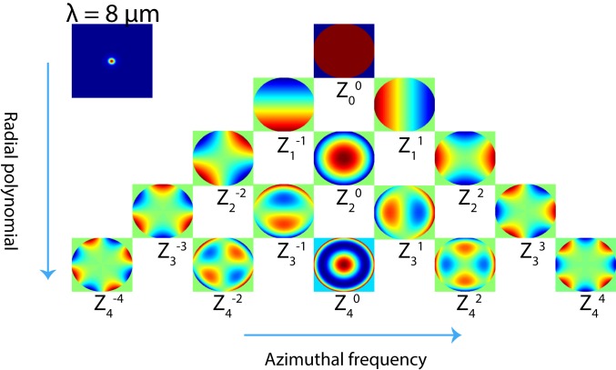
We utilized the simulated wavefront after the MDL to compute the equivalent lens aberrations. The aberrations are defined as the difference between the simulated wavefront and the ideal spherical wavefront, and the difference is expressed as a linear sum of Zernike polynomials. The coefficients of the Zernike polynomials are illustrated in Fig. 2 for the MDL with NA = 0.371, f = 19 mm computed at = 8 m. Similar results were obtained for the other MDLs and wavelengths, and are included in SI Appendix. These calculations confirm that MDLs exhibit aberrations that are comparable to or better than those seen in conventional refractive lenses.
Fig. 2.
Analysis of aberrations of the f = 19 mm lens (NA = 0.371) at = 8 m. The aberrations coefficients at other design wavelengths are included in SI Appendix.
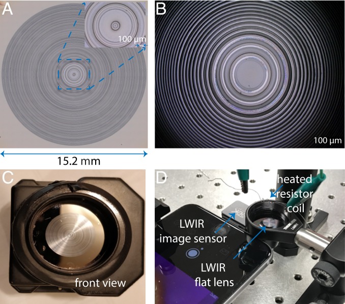
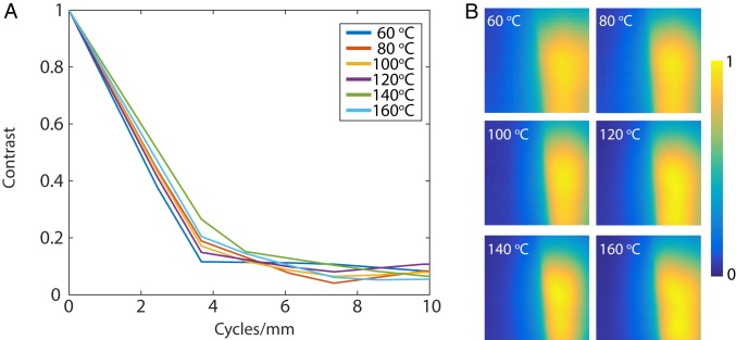
The devices were fabricated using grayscale lithography (SI Appendix) (16–18). The optical micrographs of the fabricated MDLs are shown in Fig. 3 A and B for the f = 19 and 8 mm lenses, respectively. Each lens was then assembled onto a different image sensor: Tau 2 camera core (FLIR Systems, Inc.) for f = 19 mm lens (Fig. 3C) and the LW-AAA camera (SeekThermal) for f = 8 mm lens, whose original lens was manually removed (Fig. 3D). We first characterized the modulation transfer function (MTF) of the f = 19 mm, NA = 0.371 lens coupled with the Tau 2 sensor (28). A hot plate with insulator in front was used as an object, and the MTF was estimated using the slanted edge (SI Appendix). The temperature of the hot plate was adjusted from 60 °C to 160 °C, and the results are summarized in Fig. 4. There are no significant differences in the MTF with temperature, confirming achromatic imaging.
Fig. 3.
Experiment details. Optical micrographs of the fabricated (A) f = 19 mm and (B) f = 8 mm lens. Each lens assembled onto the LWIR image sensor for (C) f = 19 mm lens with the Tau 2 sensor (FLIR Systems, Inc.) and (D) f = 8 mm lens with the LW-AAA sensor (SeekThermal).
Fig. 4.
MTF of lens with f = 19 mm, NA = 0.371 and Tau 2 image sensor (FLIR Systems, Inc.). (A) MTF curves for different temperatures show good consistency. (B) Raw images used to compute the MTF curves.
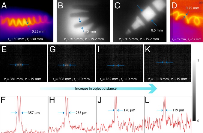
Several images were taken with both cameras for characterization, and these are summarized in Fig. 5. All figures except Fig. 5D are with the f = 19 mm lens and Tau 2 camera (FLIR Systems, Inc.), while Fig. 5D is with the f = 8 mm lens and LW-AAA (Seek Thermal) camera. Fig. 5 A and D is of a heated resistor coil, whose diameter is ∼250 m. The object distance and the image distance for each image are labeled in the corresponding figure. By placing a metal block with holes in front of a hot plate (80 °C) at various object distances, we can estimate the resolving power of the camera as indicated in Fig. 5 E–L. When the object is 762 mm away from the lens, the demagnified image of the holes is spaced by 170 m and these are still well resolved. This spacing corresponds to 10 pixels on the image sensor and represents an angular resolution of 0.013°. The field of view of the images is about 35°× 30° in the horizontal and vertical axes, respectively. Several videos are also obtained from both cameras and have been included in SI Appendix. These include videos of a resistor coil (see Movies S1 and S2 from the Tau 2 and the LW-AAA cameras, respectively), and a human subject indoors (Movie S3) and outdoors (at night; Movie S4).
Fig. 5.
Exemplary images taken using the flat-lens LWIR cameras. (A–C and E, G, I, and K) Images are taken with the f = 19 mm lens and Tau 2 core, and (D) image is with f = 8 mm and the LW-AAA camera. Object distance = and image distance = are labeled in the figures. (E, G, I, and K) The images and (F, H, J, and L) corresponding linescans of 2 holes in a metal block placed in front of a hot plate heated to 80 °C taken at increasing distances from the camera. The holes are well resolved at a distance as large as 762 mm, which corresponds to an angular resolution of 0.013°.
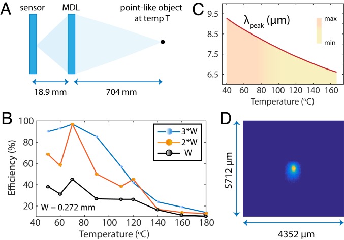
For imaging efficiency measurements, we used a sharp nail as the object (tip diameter = 4.5 mm). The nail was heated to a desired temperature and imaged onto the Tau 2 camera core (FLIR Systems, Inc.) (see SI Appendix for details and Fig. 6A). The imaging efficiency was estimated as the ratio of the sum of the pixel values inside the spot size to the sum of all of the pixel values in the entire frame. The results are summarized in Fig. 6B. An example image at 50 °C is shown in Fig. 6C. The imaging efficiency was estimated using spot size of W, 2W, and 3W as shown in Fig. 6B, where W = 0.272 mm, the FWHM of the demagnified image of the tip of the heated nail. Note that the imaging efficiency is distinct from the focusing efficiency, due to the finite size and temperature of the object that is being imaged. In all cases, the efficiency peaks approximately below 60 °C. This can be understood by appealing to Wein’s law, which determines the peak emission wavelength of a black body at a given temperature (Fig. 6D). For temperatures above 60 °C, the peak wavelength is shorter than 8 m, which is below the designed spectrum of the MDL, and, as expected, the efficiency drops. This is further exacerbated by the spectral response of the image sensor, which drops off below 8 m. Increased focusing efficiency will also lead to better-quality images. This can be readily seen by noting that power that is not focused into the main lobe essentially causes background noise and therefore reduces contrast of the image. An ideal singlet refractive lens or an ideal blazed diffractive lens can both achieve very close to 100% focusing efficiency at one wavelength. Although it is difficult to quantify a single cutoff value for efficiency (since that is dependent upon many other factors, including sensor characteristics and the image postprocessing pipeline), we can generally state that better efficiency leads to better images.
Fig. 6.
Characterization of focusing efficiency. (A) Schematic of experiment. (B) Imaging efficiency of f = 19 mm lens with Tau 2 camera core as a function of the object (hot plate) temperature. (C) Peak wavelength corresponding to a blackbody temperature using Wein’s law, showing that efficiency peak occurs for temperatures of 50 °C, which corresponds to m. (D) Exemplary point-spread function at 50 °C (raw data).
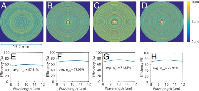
From such a perspective, one can utilize higher refractive index material to increase the focusing efficiency. Since Si exhibits high refractive index and low absorption in the LWIR band (3.42 at = 8 m), it is a good candidate material. We designed several MDLs using Si with focal length and NA equal to 19 mm and 0.371, respectively. The MDLs were designed with height level constraints of 8, 16, 32, and 64 with the corresponding optimized height profiles as shown in Fig. 7 A–D. The corresponding plots of focusing efficiency as function of wavelength are shown in Fig. 7 E–H. Simulated PSFs of all lenses are included in SI Appendix. With 8 height levels, the Si lens performs approximately equally to the polymer lens with 100 height levels. Once we increase the number of height levels in the Si lens to 16 or higher, the focusing efficiency averaged over all wavelengths is increased significantly to over 71%. Finally, we noticed that the wavelength-averaged efficiency does not increase significantly beyond 16 levels. Sixteen height levels in Si may be achieved by 4 lithography and etch steps, which are very standard processes in semiconductor manufacturing (29). Although this fabrication approach will be more expensive than imprinting directly onto a polymer, in some applications, the additional cost is likely to be justifiable.
Fig. 7.
The optimized height profile of Si MDL for NA = 0.371 and focal length = 19 mm with (A) 8 levels, (B) 16 levels, (C) 32 levels, and (D) 64 levels. The corresponding simulated focusing efficiencies for the MDL with (E) 8 levels, (F) 16 levels, (G) 32 levels, and (H) 64 levels. It is observed that the focusing efficiency tends to improve only marginally beyond 16 levels in this case. All other design parameters are the same.
Conclusion
Reducing the weight, thickness, and number of optical elements will have important applications for all spectral bands. Here, we demonstrate that this can be achieved in the LWIR band using MDLs. We note that our MDLs are quite distinct from conventional diffractive lenses because of their achromaticity. Nevertheless, conventional diffractive lenses are designed for a specific wavelength, and their focusing performance drastically drops at wavelengths away from the design value.
Materials and Methods
Design and Optimization.
All MDL designs were obtained using nonlinear optimization using a modified gradient-descent based search algorithm that maximized wavelength-averaged focusing efficiency.
Supplementary Material
Acknowledgments
We thank Brian Baker, Steve Pritchett, and Christian Bach for fabrication advice; and Tom Tiwald (Woollam) for measuring dispersion of materials. The support and resources with the computing facilities from the Center for High Performance Computing at the University of Utah and Amazon Web Services Award 051241749381 are gratefully acknowledged. R.M. and B.S.-R. acknowledge funding from the Office of Naval Research Grant N66001-10-1-4065 and from, respectively, NSF Grants ECCS 1828480 and ECCS 1936729.
Footnotes
Competing interest statement: R.M. is cofounder of Oblate Optics, Inc., which is commercializing technology discussed in this manuscript. The University of Utah has filed for patent protection for technology discussed in this manuscript.
This article is a PNAS Direct Submission.
This article contains supporting information online at www.pnas.org/lookup/suppl/doi:10.1073/pnas.1908447116/-/DCSupplemental.
References
- 1.Vollmer M., Möllmann K.-P., Infrared Thermal Imaging: Fundamentals, Research and Applications (Wiley, 2017). [Google Scholar]
- 2.Kaplan H., Practical Applications of Infrared Thermal Sensing and Imaging Equipment (SPIE Press, 2007), vol. 75. [Google Scholar]
- 3.Kateb B., Yamamoto V., Yu C., Grundfest W., Gruen J. P., Infrared thermal imaging: A review of the literature and case report. NeuroImage, 47, T154–T162 (2009). [DOI] [PubMed] [Google Scholar]
- 4.Vadivambal R., Jayas D. S., Applications of thermal imaging in agriculture and food industry—A review. Food Bioprocess Technol. 4, 186–199 (2011). [Google Scholar]
- 5.Soref R., Mid-infrared photonics in silicon and germanium. Nat. Photon. 4, 495–497 (2010). [Google Scholar]
- 6.Shakhatreh H., et al. , Unmanned aerial vehicles (UAVs): A survey on civil applications and key research challenges. IEEE Access 7, 48572–48634 (2019). [Google Scholar]
- 7.Salmon D. M., Harrison M. F., Neary J. P., Neck pain in military helicopter aircrew and the role of exercise therapy. Aviat. Space Environ. Med. 82, 978–987 (2011). [DOI] [PubMed] [Google Scholar]
- 8.Yu N., et al. , Light propagation with phase discontinuities: Generalized laws of reflection and refraction. Science 334, 333–337 (2011). [DOI] [PubMed] [Google Scholar]
- 9.Ni X., Emani N. K., Kildishev A. V., Boltasseva A., Shalaev V. M., Broadband light bending with plasmonic nanoantennas. Science 335, 427 (2012). [DOI] [PubMed] [Google Scholar]
- 10.Arbabi A., Horie Y., Bagheri M., Faraon A., Dielectric metasurfaces for complete control of phase and polarization with subwavelength spatial resolution and high transmission. Nat. Nanotechnol. 10, 937–943 (2015). [DOI] [PubMed] [Google Scholar]
- 11.Fan Q., et al. , A high numerical aperture, polarization-insensitive metalens for long-wavelength infrared imaging. Appl. Phys. Lett. 113, 201104 (2018). [Google Scholar]
- 12.Liu M., Fan Q., Yu L., Xu T., Polarization-independent infrared micro-lens array based on all-silicon metasurfaces. Opt. Express 27, 10738–10744 (2019). [DOI] [PubMed] [Google Scholar]
- 13.Banerji S., et al. , Imaging with flat optics: Metalenses or diffractive lenses? Optica 6, 805–810 (2019). [Google Scholar]
- 14.Banerji S., Sensale-Rodriguez B., A computational design framework for efficient, fabrication error-tolerant, planar THz diffractive optical elements. Sci. Rep. 9, 5801 (2019). [DOI] [PMC free article] [PubMed] [Google Scholar]
- 15.Banerji S., Sensale-Rodriguez B., “3D-printed diffractive terahertz optical elements through computational design” in Micro-and Nanotechnology Sensors, Systems, and Applications XI, Chatard Jean-Pierre, Dennis Peter N. J., Eds. (International Society for Optics and Photonics, 2019), vol. 10982, p. 109822X. [Google Scholar]
- 16.Wang P., Mohammad N., Menon R., Chromatic-aberration-corrected diffractive lenses for ultra-broadband focusing. Sci. Rep. 6, 21545 (2016). [DOI] [PMC free article] [PubMed] [Google Scholar]
- 17.Mohammad N., Meem M., Shen B., Wang P., Menon R., Broadband imaging with one planar diffractive lens. Sci. Rep. 8, 2799 (2018). [DOI] [PMC free article] [PubMed] [Google Scholar]
- 18.Meem M., Majumder A., Menon R., Full-color video and still imaging using two flat lenses. Opt. Express 26, 26866–26871 (2018). [DOI] [PubMed] [Google Scholar]
- 19.Xu K., et al. , Flexible devices fabricated by a plate-to-roll nanoimprint lithography system. Nanotechnology 30, 075301 (2018). [DOI] [PubMed] [Google Scholar]
- 20.Manaf A. R. A., Sugiyama T., Yan J., Design and fabrication of Si-HDPE hybrid Fresnel lenses for infrared imaging systems. Opt. Express 25, 1202–1220 (2017). [DOI] [PubMed] [Google Scholar]
- 21.Grulois T., et al. , Extra-thin infrared camera for low-cost surveillance applications. Opt. Lett. 39, 3169–3172 (2014). [DOI] [PubMed] [Google Scholar]
- 22.Giles M. B., Pierce N. A., An introduction to the adjoint approach to design. Flow Turbul. Combust. 65, 393–415 (2000). [Google Scholar]
- 23.Plessix R.-E., A review of the adjoint-state method for computing the gradient of a functional with geophysical applications. Geophys. J. Int. 167, 495–503 (2006). [Google Scholar]
- 24.Lalau-Keraly C. M., Bhargava S., Miller O. D., Yablonovitch E., Adjoint shape optimization applied to electromagnetic design. Opt. Express 21, 21693–21701 (2013). [DOI] [PubMed] [Google Scholar]
- 25.Molesky S., et al. , Inverse design in nanophotonics. Nat. Photon. 12, 659–670 (2018). [Google Scholar]
- 26.Hughes T. W., Minkov M., Williamson I. A. D., Fan S., Adjoint method and inverse design for nonlinear nanophotonic devices. ACS Photon. 5, 4781–4787 (2018). [Google Scholar]
- 27.Arbabi A., Horie Y., Ball A. J., Bagheri M., Faraon A., Subwavelength-thick lenses with high numerical apertures and large efficiency based on high-contrast transmitarrays. Nat. Commun. 6, 7069 (2015). [DOI] [PubMed] [Google Scholar]
- 28.Estribeau M., Magnan P., “Fast MTF measurement of CMOS imagers using ISO 12333 slanted-edge methodology” in Detectors and Associated Signal Processing, Chatard Jean-Pierre, Dennis Peter N. J., Eds. (International Society for Optics and Photonics, 2004), vol. 5251, pp. 243–253. [Google Scholar]
- 29.Swanson G. J., “Binary optics technology: The theory and design of multi-level diffractive optical elements” (Tech. Rep. 854, Massachusetts Institute of Technology Lexington Lincoln Laboratory, 1989).
Associated Data
This section collects any data citations, data availability statements, or supplementary materials included in this article.


