

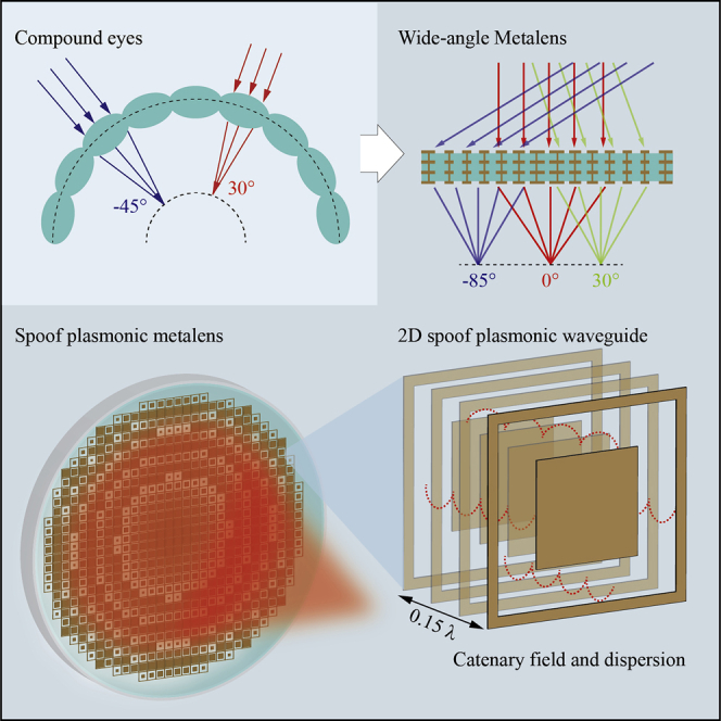
Summary
Although tremendous efforts have been devoted to investigating the analogy between the surface plasmon polariton and its spoof counterparts, it remains elusive that a single thin spoof plasmonic metalens realizes wide-angle focusing and wide field-of-view (FOV) imaging. Here, we propose a spoof plasmonic metasurface that can impart arbitrary phase with high transmittance, which comprises two-dimensional (2D) gradient spoof-insulator-spoof waveguides. With the developed catenary field and dispersion theory, their intrinsic physics is theoretically analyzed. As a proof of concept, a spoof plasmonic metalens with a thickness of 0.15λ has been elaborately designed and experimentally demonstrated for wide-angle (∼170°) focusing and wide FOV (∼40°) imaging. To the best of our knowledge, it is the first experimental demonstration of wide FOV imaging of a 2D object with single thin and planar metalens in the microwave regime. The proposed method offers a promising solution to compact cameras, integrated imaging, and detection systems.
Subject Areas: Optical Imaging, Electromagnetic Waves, Surface
Graphical Abstract
Highlights
-
•
Thin spoof metalens has been developed
-
•
A satisfactory qualitative description through catenary dispersion theory
-
•
Wide-angle microwave focusing (170°) and wide FOV (40°) imaging of 2D objects
Optical Imaging; Electromagnetic Waves; Surface
Introduction
Since the turn of this century, numerous anomalous optical phenomena associated with subwavelength metallic structures have been discovered, e.g., extraordinary optical transmission (Ebbesen et al., 1998), optical beaming effects (Lezec et al., 2002), as well as extraordinary Young interferences (Luo and Ishihara, 2004a, Pu et al., 2018a), just to name a few. Subsequent investigations reveal that these abnormal phenomena are closely related to the excitation of surface plasmon polaritons (SPPs), which are intrinsically a kind of collective oscillation of photons and electrons at the interface of metal and dielectric and attenuate exponentially in the direction perpendicular to the interface, as indicated in Figure 1A. Thanks to this unique property, SPPs could surpass the traditional diffraction limit and were taken as the next chip-scale technology (Zia et al., 2006).
Figure 1.

Concepts of SPPs and Their Spoof Analogues
(A–E) SPP confined (A) along a semi-infinite metal-dielectric interface and (B) in metal-insulator-metal (MIM) waveguide. (C) Gradient plasmon metasurfaces composed of variable-width metallic slits. Spoof SPP confined (D) along a structured metal surface and (E) coupled structured metal surface.
(F) Schematic of spoof plasmon metasurface, a spoof analogue of plasmon metasurface.
On the other hand, a thin metallic film with negative permittivity could behave as a “poor-man's perfect lens” (Pendry, 2000) and enable the sub-diffraction imaging (Fang et al., 2005, Luo and Ishihara, 2004a), since the coupled SPPs between its two interfaces would compensate the exponential decay of high spatial frequency components. Furthermore, the effective wavelength of SPPs can be greatly reduced by decreasing the metallic film thickness (Luo and Ishihara, 2004b). The appealing short-wavelength property (Luo, 2015) leads to the plasmonic lithography turning over the 22-nm resolution node (Gao et al., 2015) with a much lower cost than the extreme UV lithography.
In comparison with the metallic film, its complementary counterpart (i.e., metal-insulator-metal [MIM] waveguide) shown in Figure 1B provides stronger confinement of SPPs and thus promises highly integrated optical devices (Bozhevolnyi et al., 2006). According to the dispersion relationship of the MIM waveguide, the phase retardation through a metallic slit would increase with the shrinking slit width, and a planar and ultrathin metasurface can be developed by etching gradient metallic slits in a metallic film, as illustrated in Figure 1C. So far, abnormal beam deflection (Xu et al., 2008), super-resolution focusing (Verslegers et al., 2009), and vortex beam generation (Guo et al., 2016) have been demonstrated with both one-dimensional (1D) and two-dimensional (2D) gradient metallic slits. Alternatively, gradient metasurfaces can be constructed by exploiting the plasmon resonances (Chen et al., 2018, Wang et al., 2017) and spin-orbit interaction (Li et al., 2016, Pu et al., 2015) of metallic slits or antennas.
Among various functional metasurfaces, wide field-of-view (FOV) metalens is particularly intriguing owing to its potential applications in imaging devices from microscopes and telescopes to commercial cameras. Unfortunately, the FOV of a thin and planar metalens is stringently limited because of the unavoidable off-axis aberration. On the other hand, although wide FOV imaging systems inspired from animal's visual system have been developed (Kundtz and Smith, 2010, Lee and Szema, 2005, Ma and Cui, 2010, Zhao et al., 2016), the rotational-symmetry profiles cause the disadvantages of cumbersome size, considerable weight, and incompatibility with planar optical systems. Therefore, it poses a difficult dilemma for optical elements to simultaneously satisfying wide FOV and planar profile. Recently, metalenses doublets (with a separation gap of ∼1000λ) have been leveraged for wide FOV imaging of 2D object beyond 50° (Arbabi et al., 2016, Groever et al., 2017). Meanwhile, wide-angle focusing has been experimentally demonstrated at the visible bandwidth with ordered nanoapertures (Pu et al., 2017), and 1D wide-angle Fourier metalens has been proposed at the near-infrared band (Liu et al., 2018). Therefore, wide FOV imaging of a 2D object with single thin (<λ/5) metalens has remained elusive in the microwave regime, where the properties of metals approach those of a perfect electric conductor rather than a plasmon with negative permittivity, and SPPs cannot be naturally supported at the low frequencies. Spoof (or designer) SPPs were proposed by patterning periodic corrugations in original smooth metallic surfaces (Pendry et al., 2004), as indicated in Figure 1D. Subsequently, a myriad of spoof plasmonic waveguides (Hibbins et al., 2005, Ma et al., 2013, Shen et al., 2013, Williams et al., 2008, Wu et al., 2017, Zhen et al., 2018) and the spoof-insulator-spoof (SIS) waveguide (Kats et al., 2011, Zhang et al., 2015) have been developed, as shown in Figures 1D and 1E. Despite these impressive advances, nearly all of the aforementioned works focus on the in-plane spoof plasmonic waveguide devices. Therefore, a fundamental question is still to be answered, i.e., could the powerful electromagnetic manipulation competence in free space be well inherited during the spoof analogy of the plasmonic metasurface. Recently, only a few of works shed light on this question by developing 1D beam deflector and focusing metalens with spoof plasmonic metasurface (Pu et al., 2018b, Yin et al., 2019), as illustrated in Figure 1F. Nevertheless, neither of them involves the significant topic of wide-angle focusing and wide FOV imaging of a 2D object.
In this paper, a spoof plasmonic metalens that can perform wide-angle (∼170°) focusing and wide FOV (∼40°) imaging is presented to demonstrate the powerful electromagnetic manipulation ability of spoof plasmonic metasurface. The following contexts are organized as: First, the transmission properties and fundamental mode distribution of 2D SIS waveguide are investigated and its underlying physical mechanism is interpreted based on a catenary dispersion model (Pu et al., 2018b). Subsequently, the width-dependent phase modulation is, respectively, investigated by the full-wave simulations and the proposed theoretical model. Finally, a spoof plasmonic metalens with parabolic phase profile is elaborately designed, fabricated, and experimentally demonstrated for wide-angle focusing and wide FOV imaging of a 2D object.
Results and Discussions
Phase-Engineering Properties of 2D SIS Waveguides
To develop a spoof plasmonic transmissive metasurface, the key is designing a 2D SIS waveguide unit cell that can impart arbitrary phase change with high transmittance. However, there is no appropriate 2D spoof plasmonic waveguide for phase engineering and electromagnetic manipulation in free space, since the previous investigations mainly focus on the in-plane spoof plasmonic waveguide devices, which are composed of tens of periodic metallic grooves and not in the subwavelength scale along the propagation direction. Figure 2A illustrates the proposed spoof plasmonic metasurface, where each unit cell (with a period of P = 3.3 mm, ∼λ/3) consists of several ultra-thin (with a thickness of tm = 0.018 mm, ∼λ0/500) metallic patterns separated by thin (with a thickness of d = 0.508 mm, ∼λ0/20) dielectric substrates (with a dielectric constant of ϵd = 2.65 and loss tangent of 0.001). Here, the quadrate patches (with a side length of l) at the center and quadrate ring (with a width of 0.1 mm) at the margin of the unit cells form a 2D metallic slit (with a slit width of g). The alternative stacks of metal patterns and dielectric substrates mimic an SIS waveguide for generating different phase retardation by changing the slit width. The latter analysis shows that only four-layer metallic patterns and three-layer dielectric substrates are sufficient to generate a phase change covering the whole range of 2π with high transmittance. Therefore, the total length of the SIS waveguide is about 1.5 mm (∼0.15λ), which is helpful to construct ultra-thin spoof plasmonic metasurfaces.
Figure 2.

Schematic of the 2D SIS Waveguide and the Power as well as Electric Field Distribution
(A) Schematic illustration of 2D SIS waveguides with defined geometric parameters.
(B) Power flow of the SIS waveguide along the xoz plane with l = 1.5 mm.
(C) Normalized power along the dotted line shown in Figure 2B.
(D) Electric field distribution of the SIS waveguide along the xoz plane.
(E) Normalized electric field along the horizontal lines: (I) z = 0, (II) z = d, (III) z = 2d, and (IV) z = 3d.
First, we would like to investigate the field distribution in the proposed 2D SIS waveguide at a frequency of 30 GHz (λ0 = 10 mm). Owing to the C4 symmetry of the proposed structure, identical responses will be obtained under the normal incidence for transverse magnetic (TM) and electric (TE) polarizations. Subsequently, the transmission properties of the 2D SIS waveguide under the illumination of TM polarization are investigated via finite-element simulation with commercial CST software, where the unit cell and open add space boundary conditions are applied along the x, y, and z directions, respectively. Figure 2B shows the simulated vector power flow within the xoz plane when the slit width is g = 1.6 mm (i.e., l = 1.5 mm). It clearly indicates that electromagnetic waves can effectively transmit through the proposed SIS waveguide. The power flow along the cutline in Figure 2B is depicted in Figure 2C, which demonstrates that the incident wave is transformed into spoof plasmon wave at the entrance of the SIS waveguide and then transforms back into propagating wave at the exit of the SIS waveguide. The vector electric field in the xoz plane shown in Figure 2D illustrates the electric field circulating around the SIS waveguide. The magnetic dipole generated by the electric circular displacement current is parallel to the magnetic field of the incident wave (along the y axis), leading to a non-unity effective permeability, which will be taken into consideration in our theoretical model. The electric field distribution along the four metallic pattern layers in Figure 2E reveals the abrupt change of the electric field within a deep-subwavelength scale and tremendous field enhancement at the ends of the metallic slits (Huang et al., 2019, Pu et al., 2018b), which is mainly attributed to the ultralow filling ratio (η = tm/(tm + d) = 0.034) of thin metallic slit and cannot be accessed by previous SIS waveguide with a high filling ratio of 0.9 (Kats et al., 2011).
Second, the phase engineering ability of the proposed 2D SIS waveguide around 30 GHz is investigated. Because there are only three periods in our SIS waveguides, traditional Bloch dispersion relation (Rahman and Stuchly, 2001, Xu et al., 2005) is not applied. Alternatively, we take the thin metallic structure as a surface impedance layer as a simple but reasonable approximation and resort to the transfer matrix method to predict the electromagnetic response of the proposed structure (Cheng et al., 2019, Pfeiffer and Grbic, 2013). The equivalent circuit model of the metallic patch in Figure 3A is a parallel LC circuit, as indicated in Figure 3B. Therefore, the effective admittance (Ymeta) and impedance (Zmeta) of each metasurface layer can be expressed as:
| (Equation 1) |
where, ω is the incidence angular frequency. The effective inductor L and capacitance C in Equation (1) are related to the geometric parameters and operation frequency. According to the quasi-stationary field theory (Huang et al., 2019, MacFarlane, 1946), they can be respectively expressed as:
| (Equation 2) |
and
| (Equation 3) |
where ni is the effective index of the surrounding the metasurface layer. Specifically, ni = 1 for air layer and should be changed to ni = for dielectric substrate, where ϵeff = ϵd = 2.65, and μeff is the effective permeability generated by the circulating electric field mentioned earlier. The mathematical expression of F is written as:
| (Equation 4) |
Figure 3.

Equivalent Circuit Model and Transmission Properties of the Metasurface with Catenary Dispersion
(A) Schematic illustration of the metasurface.
(B) Equivalent circuit model of the metasurface.
(C) Transfer matrix model of cascading metasurfaces that support the propagation of spoof plasmon.
(D) Simulated and calculated phase of S21 changes with the incident frequency with different l.
(E) Generated effective permeability changes with l.
(F) Simulated amplitude of S21 changes with the gap width.
(G) Simulated phase of S21 changes with the gap width.
We note that the dispersions of both effective inductor L and capacitance C follow the “catenary of equal phase,” which has been utilized to generate continuous and linear geometric phases (Pu et al., 2015). Based on the physical model established in Figure 3C, we can obtain the whole transfer matrix as follows (see Transparent Methods for detail):
| (Equation 5) |
where, Z0 = 1/Y0 = 377Ω, Yd = Y0. To obtain the transmission and reflection coefficients, i.e., S21 and S11, we assume the input is [a; b] and the normalized output is [1; 0]. Then, we have:
| (Equation 6) |
and the transmission and reflection coefficients can be expressed as:
| (Equation 7) |
To check the above-mentioned theoretical analysis, the phase of S21 changes with the incident frequency and metallic patch width is calculated as shown in Figure 3D, well consistent with the full-wave simulation results. Therefore, the catenary field and dispersion theory provides a satisfactory qualitative description of the intrinsic physics of the spoof plasmonic metasurface, offering an alternative design method to time-costing brute-force simulations. The generated effective permeability varies with the metallic patch width l, as indicated in Figure 3E.
Similar to the plasmonic metasurfaces operating in the visible band (Xu et al., 2008), adjusting the width of the metallic slits is an effective way to realize local phase modulation. Figures 3F and 3G, respectively, present the simulated amplitude and phase of S21 at 30 GHz change with the slit width, indicating that nearly 2π phase shift can be realized within a thin thickness (0.15λ) by changing the slit widths from 0.25 to 1.25 mm, with the amplitudes being kept above 0.8. Note that, for a transmissive spoof metasurface within the subwavelength scale (<λ/5), it is quite difficult to obtain a phase change covering the whole range of 2π with high transmittance through single or two coupled metallic layers. To illustrate this, the amplitude and phase modulation of single and two coupled metallic layers are also investigated at 30 GHz. The phase shift of single-layer and two double-coupled layers with a separation of d and 3d are, respectively, only 50°, 90°, and 170° when the transmission coefficient is higher than 0.8 (see Figure S1 for detail), and thus cascading metallic patterns are generally needed in previous reports (Cheng et al., 2019, Pfeiffer and Grbic, 2013) to ensure a complete control of the wavefront. Otherwise, the performance of the metalens will be greatly deteriorated or even invalided in this circumstance. Because the evanescent coupling between the two ends of the metallic slits is robust to the change of incident angle (Guo et al., 2018), the relative phase shift generated by the spoof plasmonic metasurface is nearly non-variable for various incident angles (see Figure S2 for detail), which is helpful in the construction of a wide-angle metalens.
Spoof Plasmonic Metalens-Based Wide-Angle Focusing and Imaging
Here, based on the proposed spoof plasmonic metasurface, we implement the experimental demonstration of isolate spoof plasmonic metalens for wide-angle focusing (170°) and further confirm its capability of wide FOV imaging (40°) of a 2D arbitrary object. The fundamental mechanism of wide-angle focusing and imaging lies in that the proposed spoof plasmonic metalens can perform the symmetry transformation from rotational symmetry to transversal symmetry (Pu et al., 2017). For this purpose, the following quadratic phase profile should be fulfilled (Guo et al., 2018):
| (Equation 8) |
The symmetry transformation can be mathematically expressed as:
| (Equation 9) |
where r is the radial distance of the phase shift unit cell to the metalens center, θ is the oblique angle of incidence, f is the focal length of the metalens, , and . Since C is a constant that is independent of r and can be neglected, the rotational effect θ of the oblique incidence light is perfectly converted to the translational symmetry Δ of the focusing spot within the focal plane.
To verify our design, a metalens with a radius R = 200 mm (including 25,921 SIS waveguide unit cells) and a designed focal length f = 100 mm (the corresponding numerical aperture defined by NA = sin(tan−1(R/f)) is about 0.89) was fabricated on three F4B substrates with print circuit board (PCB) technique and then pressed together (see Figures S3A–S3C for detail). The focusing properties of the sample at a broadband range from 26.5 to 32 GHz are characterized by near-field measurements in an anechoic chamber with a step of 0.5 GHz. The measuring setup and method are described in the Transparent Methods section (see Figures S3D and S3E and Transparent Methods for detail). Figure 4 shows the measured intensity distributions along the xoz plane for different incident frequencies. We can see that intensive focusing spots are formed in a broadband and the focal length gradually increases with the incident frequency, with the FWHM (full-width at half magnitude) of the spots approaching the theoretical diffraction limit (∼0.61λ/NA), which demonstrates that the designed spoof plasmonic metalens can operate well in a broadband range from 26.5 to 32 GHz. The relative broadband operation band of the proposed spoof plasmonic metalens is mainly attributed to the low quality-factor of the SIS waveguide, which leads to a slow dispersion of the amplitude and phase modulation around the operation frequency (see Figure S4 for detail).
Figure 4.

Broadband Focusing Properties of the Spoof Metalens
(A–L) Measured intensity distribution in the xoz plane for normal incidences with different frequencies.
Subsequently, the wide-angle focusing properties are experimentally verified at 30 GHz. The measured intensity and phase distributions shown in Figures 5A–5E display the focusing properties for different incidence angles of θ = 0°, 30°, and 75°. Although the measured focal length (∼90 mm) at 30 GHz is slightly smaller than the design value of 100 mm, it is nearly non-variable for different incident angles. The intensity and phase distributions along the focal plane (indicated by the white dotted lines) are shown in the corresponding insets. The measured normalized intensity profiles along the center of the focal plane under different incident angles are presented in Figure 5G, which show that the focusing pattern maintains well for large-angle off-axis illumination up to 85°. These results demonstrate that the proposed spoof plasmonic metalens can realize a wide-angle focusing within 170°, considering the structural and wavefront symmetry of the proposed metalens. Note that the translational shifts under 0°, 30°, 75°, and 85° are, respectively, 0, 45, 89, and 91 mm, agreeing well with the theoretical expectations, i.e., Δ = fsin(θ), that is, 50, 96.6, and 99.6 mm, correspondingly. The small discrepancy between them may be attributed to the non-ideal plane wave emitted from the horn antenna and measurement errors. The measured focusing efficiency (defined by the intensity ratio between the focal spot and incidence) at 30 GHz is about 46%. Several factors that influence the focusing efficiency include the direct reflection due to the mismatched impedance, substrate absorptive loss, fabrication errors (e.g., the substrate thickness discrepancies and the SIS waveguides misalignment generated during the PCB board pressing), and the unsmooth transmitted wavefront caused by limited quantitative phase levels, which is especially obvious at the margin of the metalens as the phase change is abrupt. Therefore, to further improve the efficiency of the metalens, some antireflection structure may be considered in the future design and smaller unit cell with higher phase engineering accuracy is preferred, which may require cascading more layers. The distortion of the substrate can be alleviated by using harder substrate with lower loss (e.g., RF-35). To further demonstrate the unique wide-angle property of the proposed wide-angle metalens, a control experiment is also done, where the metalens is designed with the same building blocks, diameter, and focal length but a spherical phase profile (i.e.). It is shown that the focusing properties are seriously deteriorated when the incident angle increases. No obvious focusing spot is observed even for a 30° incidence (see Figure S5 for detail).
Figure 5.

Wide-Angle Focusing Properties of the Spoof Metalens
(A and B) Measured (A) intensity and (B) phase distribution in the xoz plane for normal incidence at 30 GHz. Insets show the corresponding intensity and phase distribution in the focal plane.
(C) and (D) are similar to (A) and (B) except that the incidence angle is changed to 30°.
(E) and (F) are similar to (A) and (B) except that the incidence angle is changed to 75°.
(G) Measured normalized intensity profiles along the cutline through the center of the focal plane under different incidences.
We further carry an imaging experiment of a 2D object at 30 GHz using the same metalens. As illustrated in Figure 6A, an object consisting of an “I”-shaped aperture etched in tin foil is attached on a foam plate. The outer dimensional size of the word is 35 × 60 mm2 and the characteristic width of the aperture is 6 mm (approaching the resolution limit of the designed metalens, i.e., 0.61λ/NA). Ideally, the object should be placed at a distance do from the metalens to ensure the imaging process satisfies the paraxial approximation. The FOV with a measure of 2θ is determined by observing the imaging quality of the object with a relative horizontal shift of s from the metalens center (θ = tan−1(s/do)), as illustrated in Figure S6A. However, restricted by the limited measuring space, the object distance is fixed at 180 mm in practical measurement (Figure S6B). The waveguide probe is placed at a distance of 180 mm from the metalens and steered at a step of 4 mm with an area of 200 × 200 mm2. The measured results corresponding to different illumination angles of 0°, 10°, and 20° are plotted in Figures 6B–6D. Although the imaging quality deteriorates with increasing incident angle, the proposed metalens can image the 2D object well within 40°, considering the symmetry of the metalens.
Figure 6.

Wide FOV Imaging Properties of the Spoof Metalens
(A) Photography of the measurement setup, where both the objective and detection distances do are 180 mm. The outer dimensional size of the object, an “I”-shaped aperture etched in silver paper, is 35 × 60 mm2 and the width of the aperture is 6 mm.
(B–D) Measured imaging results at 30 GHz with different relative horizontal shift s from the metalens center s = dotan(θ).
Generally, the focal length is fixed once the metalens has been fabricated, which is not feasible for application in commercial cameras and advanced optical systems, where focal adjustment and zooming are universal features. Varifocal systems were first developed by changing the axial distance between multiple conventional bulky refractive elements with a sophisticated optical design strategy and then implemented based on the shape change of deformable solid (Shian et al., 2013) and liquid-filled lenses (Chronis et al., 2003, Sugiura and Morita, 1993) systems with a slow tuning speed. Although liquid crystal-based electrically varifocal lenses exhibit a more compact footprint and higher tuning speeds (Ren and Wu, 2006, Ren et al., 2007), the large pixel size of diffractive optical elements may limit the imaging performance. Recently, continuous varifocal metalens has been demonstrated by reconfigurable metasurfaces integrating with stretchable substrate (Ee and Agarwal, 2016), lateral actuation (She et al., 2018), and microelectromechanical systems (Arbabi et al., 2018). For the proposed design here, a possible approach to realizing the varifocal design is inserting varactor and PIN (positive-insulator-negative) diodes in the gaps between the inner and outer metallic patterns. By changing the external bias voltage, the states of the varactor and PIN diodes can be electrically harnessed, imparting different inductor and capacitor to the effective impedance of metasurface. Consequently, both the amplitude and phase of the transmitted wave can be adjusted according to the catenary dispersion theory, which will be studied in our future investigation.
Conclusion
In summary, a 2D spoof plasmonic metasurface composed of variable-width SIS waveguides, as corresponding analogue of the plasmonic metallic slits metasurface, has been proposed to construct thin and planar microwave lens antenna. The developed catenary field and dispersion theory provides a satisfactory qualitative description of the intrinsic physics of the spoof plasmonic metasurface, offering an alternative optimization method to time-costing brute-force simulations. As a representational prototype, a single thin spoof plasmonic metalens with the competence of symmetry transformation from rotational symmetry to transversal symmetry has been fabricated and experimentally demonstrated for wide-angle microwave focusing (170°) and imaging (40°). These results reveal a roadmap toward future compact, portable, and wide FOV camera.
Limitations of the Study
A moderate FOV of 40° is demonstrated here for 2D object imaging. In addition, the focal length is fixed once the metalens has been fabricated and then the maximum FOV is also determined. Therefore, a metalens with a large NA is generally needed for wide FOV imaging, for example, the NA is about 0.89 in our design. Further study will be needed to address these issues.
Methods
All methods can be found in the accompanying Transparent Methods supplemental file.
Acknowledgments
This work was supported by the National Natural Science Funds of China under Grant Nos. 61875253, 61575032, and 61622508.
Author Contributions
Y.G. conceived the original idea. Y.G. and M.P. performed the theoretical calculations and the numerical simulations. Z.Z., X.L., and X.M. fabricated the sample and performed the experimental measurements and data analysis. X.L. supervised the whole project. Y.G. wrote the manuscript, and all the authors reviewed the manuscript.
Declaration of Interests
The authors declare there is no competing interest.
Published: November 22, 2019
Footnotes
Supplemental Information can be found online at https://doi.org/10.1016/j.isci.2019.10.019.
Supplemental Information
References
- Arbabi A., Arbabi E., Kamali S.M., Horie Y., Han S., Faraon A. Miniature optical planar camera based on a wide-angle metasurface doublet corrected for monochromatic aberrations. Nat. Commun. 2016;7:13682. doi: 10.1038/ncomms13682. [DOI] [PMC free article] [PubMed] [Google Scholar]
- Arbabi E., Arbabi A., Kamali S.M., Horie Y., Faraji-Dana M., Faraon A. MEMS-tunable dielectric metasurface lens. Nat. Commun. 2018;9:812. doi: 10.1038/s41467-018-03155-6. [DOI] [PMC free article] [PubMed] [Google Scholar]
- Bozhevolnyi S.I., Volkov V.S., Devaux E., Laluet J.-Y., Ebbesen T.W. Channel plasmon subwavelength waveguide components including interferometers and ring resonators. Nature. 2006;440:508–511. doi: 10.1038/nature04594. [DOI] [PubMed] [Google Scholar]
- Chen Y., Gao J., Yang X. Direction-controlled bifunctional metasurface polarizers. Laser Photon. Rev. 2018;12:1800198. [Google Scholar]
- Cheng K., Wei Z., Fan Y., Zhang X., Wu C., Li H. Realizing broadband transparency via manipulating the hybrid coupling modes in metasurfaces for high-efficiency metalens. Adv. Opt. Mater. 2019;7:1900016. [Google Scholar]
- Chronis N., Liu G.L., Jeong K.-H., Lee L.P. Tunable liquid-filled microlens array integrated with microfluidic network. Opt. Express. 2003;11:2370–2378. doi: 10.1364/oe.11.002370. [DOI] [PubMed] [Google Scholar]
- Ebbesen T.W., Lezec H.J., Ghaemi H.F., Thio T., Wolff P.A. Extraordinary optical transmission through sub-wavelength hole arrays. Nature. 1998;391:667–669. [Google Scholar]
- Ee H.-S., Agarwal R. Tunable metasurface and flat optical zoom lens on a stretchable substrate. Nano Lett. 2016;16:2818–2823. doi: 10.1021/acs.nanolett.6b00618. [DOI] [PubMed] [Google Scholar]
- Fang N., Lee H., Sun C., Zhang X. Sub-diffraction-limited optical imaging with a silver superlens. Science. 2005;308:534–537. doi: 10.1126/science.1108759. [DOI] [PubMed] [Google Scholar]
- Gao P., Yao N., Wang C., Zhao Z., Luo Y., Wang Y., Gao G., Liu K., Zhao C., Luo X. Enhancing aspect profile of half-pitch 32 nm and 22 nm lithography with plasmonic cavity lens. Appl. Phys. Lett. 2015;106:093110. [Google Scholar]
- Groever B., Chen W.T., Capasso F. Meta-lens doublet in the visible region. Nano Lett. 2017;17:4902–4907. doi: 10.1021/acs.nanolett.7b01888. [DOI] [PubMed] [Google Scholar]
- Guo Y., Pu M., Zhao Z., Wang Y., Jin J., Gao P., Li X., Ma X., Luo X. Merging geometric phase and plasmon retardation phase in continuously shaped metasurfaces for arbitrary orbital angular momentum generation. ACS Photon. 2016;3:2022–2029. [Google Scholar]
- Guo Y., Ma X., Pu M., Li X., Zhao Z., Luo X. High-efficiency and wide-angle beam steering based on catenary optical fields in ultrathin metalens. Adv. Opt. Mater. 2018;6:1800592. [Google Scholar]
- Hibbins A.P., Evans B.R., Sambles J.R. Experimental verification of designer surface plasmons. Science. 2005;308:670. doi: 10.1126/science.1109043. [DOI] [PubMed] [Google Scholar]
- Huang Y., Luo J., Pu M., Guo Y., Zhao Z., Ma X., Li X., Luo X. Catenary electromagnetics for ultrabroadband lightweight absorbers and large-scale flat antennas. Adv. Sci. 2019;6:1801691. doi: 10.1002/advs.201801691. [DOI] [PMC free article] [PubMed] [Google Scholar]
- Kats M.A., Woolf D., Blanchard R., Yu N., Capasso F. Spoof plasmon analogue of metal-insulator-metal waveguides. Opt. Express. 2011;19:14860–14870. doi: 10.1364/OE.19.014860. [DOI] [PubMed] [Google Scholar]
- Kundtz N., Smith D.R. Extreme-angle broadband metamaterial lens. Nat. Mater. 2010;9:129–132. doi: 10.1038/nmat2610. [DOI] [PubMed] [Google Scholar]
- Lee L.P., Szema R. Inspirations from biological optics for advanced photonic systems. Science. 2005;310:1148–1150. doi: 10.1126/science.1115248. [DOI] [PubMed] [Google Scholar]
- Lezec H.J., Degiron A., Devaux E., Linke R.A., Martin-Moreno L., Garcia-Vidal F.J., Ebbesen T.W. Beaming light from a subwavelength aperture. Science. 2002;297:820–822. doi: 10.1126/science.1071895. [DOI] [PubMed] [Google Scholar]
- Li X., Chen L., Li Y., Zhang X., Pu M., Zhao Z., Ma X., Wang Y., Hong M., Luo X. Multicolor 3D meta-holography by broadband plasmonic modulation. Sci. Adv. 2016;2:e1601102. doi: 10.1126/sciadv.1601102. [DOI] [PMC free article] [PubMed] [Google Scholar]
- Liu W., Li Z., Cheng H., Tang C., Li J., Zhang S., Chen S., Tian J. Metasurface enabled wide-angle fourier Lens. Adv. Mater. 2018;30:1706368. doi: 10.1002/adma.201706368. [DOI] [PubMed] [Google Scholar]
- Luo X. Principles of electromagnetic waves in metasurfaces. Sci. China Phys. Mech. Astron. 2015;58:594201. [Google Scholar]
- Luo X., Ishihara T. Surface plasmon resonant interference nanolithography technique. Appl. Phys. Lett. 2004;84:4780–4782. [Google Scholar]
- Luo X., Ishihara T. Subwavelength photolithography based on surface-plasmon polariton resonance. Opt. Express. 2004;12:3055–3065. doi: 10.1364/opex.12.003055. [DOI] [PubMed] [Google Scholar]
- Ma H., Cui T. Three-dimensional broadband and broad-angle transformation-optics lens. Nat. Commun. 2010;1:124. doi: 10.1038/ncomms1126. [DOI] [PubMed] [Google Scholar]
- Ma H.F., Shen X., Cheng Q., Jiang W.X., Cui T.J. Broadband and high-efficiency conversion from guided waves to spoof surface plasmon polaritons. Laser Photon. Rev. 2013;8:146–151. [Google Scholar]
- MacFarlane G.G. Quasi-stationary field theory and its application to diaphragms and junctions in transmission lines and wave guides. Proc. Inst. Elect. Eng. Lond. U.K. 1946;93:703–719. [Google Scholar]
- Pendry J.B. Negative refraction makes a perfect lens. Phys. Rev. Lett. 2000;85:3966–3969. doi: 10.1103/PhysRevLett.85.3966. [DOI] [PubMed] [Google Scholar]
- Pendry J.B., Martin-Moreno L., Garcia-Vidal F.J. Mimicking surface plasmons with structured surfaces. Science. 2004;305:847–848. doi: 10.1126/science.1098999. [DOI] [PubMed] [Google Scholar]
- Pfeiffer C., Grbic A. Cascaded metasurfaces for complete phase and polarization control. Appl. Phys. Lett. 2013;102:231116. [Google Scholar]
- Pu M., Li X., Ma X., Wang Y., Zhao Z., Wang C., Hu C., Gao P., Huang C., Ren H. Catenary optics for achromatic generation of perfect optical angular momentum. Sci. Adv. 2015;1:e1500396. doi: 10.1126/sciadv.1500396. [DOI] [PMC free article] [PubMed] [Google Scholar]
- Pu M., Li X., Guo Y., Ma X., Luo X. Nanoapertures with ordered rotations: symmetry transformation and wide-angle flat lensing. Opt. Express. 2017;25:31471–31477. doi: 10.1364/OE.25.031471. [DOI] [PubMed] [Google Scholar]
- Pu M., Guo Y., Li X., Ma X., Luo X. Revisitation of extraordinary Young’s interference: from catenary optical fields to spin-orbit interaction in metasurfaces. ACS Photon. 2018;5:3198–3204. [Google Scholar]
- Pu M., Ma X., Guo Y., Li X., Luo X. Theory of microscopic meta-surface waves based on catenary optical fields and dispersion. Opt. Express. 2018;26:19555–19562. doi: 10.1364/OE.26.019555. [DOI] [PubMed] [Google Scholar]
- Rahman M., Stuchly M.A. Transmission line–periodic circuit representation of planar microwave photonic bandgap structures. Microwave Opt. Technol. Lett. 2001;30:15–19. [Google Scholar]
- Ren H., Wu S.-T. Adaptive liquid crystal lens with large focal length tunability. Opt. Express. 2006;14:11292–11298. doi: 10.1364/oe.14.011292. [DOI] [PubMed] [Google Scholar]
- Ren H., Fox D.W., Wu B., Wu S.-T. Liquid crystal lens with large focal length tunability and low operating voltage. Opt. Express. 2007;15:11328–11335. doi: 10.1364/oe.15.011328. [DOI] [PubMed] [Google Scholar]
- She A., Zhang S., Shian S., Clarke D.R., Capasso F. Adaptive metalenses with simultaneous electrical control of focal length, astigmatism, and shift. Sci. Adv. 2018;4:eaap9957. doi: 10.1126/sciadv.aap9957. [DOI] [PMC free article] [PubMed] [Google Scholar]
- Shen X., Cui T.J., Martin-Cano D., Garcia-Vidal F.J. Conformal surface plasmons propagating on ultrathin and flexible films. Proc. Natl. Acad. Sci. U S A. 2013;110:40. doi: 10.1073/pnas.1210417110. [DOI] [PMC free article] [PubMed] [Google Scholar]
- Shian S., Diebold R.M., Clarke D.R. Tunable lenses using transparent dielectric elastomer actuators. Opt. Express. 2013;21:8669–8676. doi: 10.1364/OE.21.008669. [DOI] [PubMed] [Google Scholar]
- Sugiura N., Morita S. Variable-focus liquid-filled optical lens. Appl. Opt. 1993;32:4181–4186. doi: 10.1364/AO.32.004181. [DOI] [PubMed] [Google Scholar]
- Verslegers L., Catrysse P.B., Yu Z., White J.S., Barnard E.S., Brongersma M.L., Fan S. Planar lenses based on nanoscale slit arrays in a metallic film. Nano Lett. 2009;9:235–238. doi: 10.1021/nl802830y. [DOI] [PubMed] [Google Scholar]
- Wang S., Wu P.C., Su V.-C., Lai Y.-C., Hung Chu C., Chen J.-W., Lu S.-H., Chen J., Xu B., Kuan C.-H. Broadband achromatic optical metasurface devices. Nat. Commun. 2017;8:187. doi: 10.1038/s41467-017-00166-7. [DOI] [PMC free article] [PubMed] [Google Scholar]
- Williams C.R., Andrews S.R., Maier S.A., Fernández-Domínguez A.I., Martín-Moreno L., García-Vidal F.J. Highly confined guiding of terahertz surface plasmon polaritons on structured metal surfaces. Nat. Photon. 2008;2:175. [Google Scholar]
- Wu X., Meng Y., Tian J., Huang Y., Xiang H., Han D., Wen W. Direct observation of valley-polarized topological edge states in designer surface plasmon crystals. Nat. Commun. 2017;8:1304. doi: 10.1038/s41467-017-01515-2. [DOI] [PMC free article] [PubMed] [Google Scholar]
- Xu T., Wang C., Du C., Luo X. Plasmonic beam deflector. Opt. Express. 2008;16:4753–4759. doi: 10.1364/oe.16.004753. [DOI] [PubMed] [Google Scholar]
- Xu X., Xi Y., Han D., Liu X., Zi J., Zhu Z. Effective plasma frequency in one-dimensional metallic-dielectric photonic crystals. Appl. Phys. Lett. 2005;86:091112. [Google Scholar]
- Yin X., Zhu H., Guo H., Deng M., Xu T., Gong Z., Li X., Hang Z.H., Wu C., Li H. Hyperbolic metamaterial devices for wavefront manipulation. Laser Photon. Rev. 2019;13:1800081. [Google Scholar]
- Zhang H.C., Cui T.J., Zhang Q., Fan Y., Fu X. Breaking the challenge of signal integrity using time-domain spoof surface plasmon polaritons. ACS Photon. 2015;2:1333–1340. [Google Scholar]
- Zhao Y.-Y., Zhang Y.-L., Zheng M.-L., Dong X.-Z., Duan X.-M., Zhao Z.-S. Three-dimensional Luneburg lens at optical frequencies. Laser Photon. Rev. 2016;10:665–672. [Google Scholar]
- Zhen G., Wu L., Gao F., Luo Y., Zhang B. Spoof plasmonics: from metamaterial concept to topological description. Adv. Mater. 2018;30:1706683. doi: 10.1002/adma.201706683. [DOI] [PubMed] [Google Scholar]
- Zia R., Schuller J.A., Chandran A., Brongersma M.L. Plasmonics: the next chip-scale technology. Mater. Today. 2006;9:20–27. [Google Scholar]
Associated Data
This section collects any data citations, data availability statements, or supplementary materials included in this article.