Abstract
Due to their inherent physical properties, thin-film Si/SiGe heterostructures have specific thermal management applications in advanced integrated circuits and this in turn is essential not only to prevent a high local temperature and overheat inside the circuit, but also generate electricity through the Seebeck effect. Here, we were able to enhance the Seebeck effect in the germanium composite quantum dots (CQDs) embedded in silicon by increasing the number of thin silicon layers inside the dot (multi-fold CQD material). The Seebeck effect in the CQD structures and multi-layer boron atomic layer-doped SiGe epitaxial films was studied experimentally at temperatures in the range from 50 to 300 K and detailed calculations for the Seebeck coefficient employing different scattering mechanisms were made. Our results show that the Seebeck coefficient is enhanced up to ≈40% in a 3-fold CQD material with respect to 2-fold Ge/Si CQDs. This enhancement was precisely modeled by taking into account the scattering of phonons by inner boundaries and the carrier filtering by the CQD inclusions. Our model is also able to reproduce the observed temperature dependence of the Seebeck coefficient in the B atomic layer-doped SiGe fairly well. We expect that the phonon scattering techniques developed here could significantly improve the thermoelectric performance of Ge/Si materials through further optimization of the layer stacks inside the quantum dot and of the dopant concentrations.
Subject terms: Thermoelectric devices and materials, Quantum dots
Introduction
Due to dense packaging in high power electronics, the heat generation in chips can reach ~50 W/cm2, which produces uneven temperature distributions with 5 °C to 30 °C overheated hot spots and decreases the reliability of silicon-based electronic components1–3. These hot spots can generate electricity through the Seebeck effect by harvesting waste heat from electronic circuits. Through the reverse Peltier effect, on-chip cooling has been achieved in thin-film Si/SiGe superlattice micro-refrigerators, which allows effective on-chip temperature control3.
The thermoelectric efficiency is most conveniently determined by the figure of merit, Z = S2/κρ, where S is the Seebeck coefficient, κ is the thermal conductivity and ρ is the electrical resistivity. Therefore, the better thermoelectric performance can be obtained at greater Z, requiring greater S and smaller κ and ρ. The search for efficient thermoelectric materials is challenging due to the multitude of conflicting property requirements that must be simultaneously satisfied, which is because the coefficients S, ρ and κ are usually related to one another and are not mutually exclusive4. Figure 1 compares the variation of S and Z as a function of the electrical resistivity. It is seen that increasing ρ enhances the Seebeck coefficient while much smaller optimal electrical resistivities, corresponding to the dopant concentrations of about 1020–1021 cm−3 in Fig. 1, maximizes the figure of merit.
Figure 1.
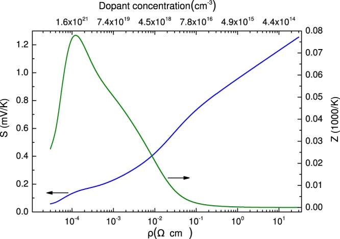
Variation of the Seebeck coefficient and figure of merit upon electrical resistivity for a bulk Si at T = 300 K. Theoretical estimates are made using the works of Yi and Yu47 and Morelli et al.59. Relaxation time τp is obtained by taking into account phonon-phonon and Umklapp scattering, phonon-alloy and boundary scattering. τe takes into account electron scattering by impurities and phonons.
Improving Seebeck coefficient is very relevant to numerous applications utilizing thin-film approach to achieve thermoelectric sensing functionality2,5. One common strategy for increasing S relies on the enhancement of the phonon scattering, which is ultimately governed by interfaces and boundaries in nanostructured materials2,6–8.
In particular, Choi et al. reported thermoelectric Te-embedded Bi2Te3 materials with enhanced scattering of phonons at the inter-grain Te/Bi2Te3 boundaries9. Ahmad et al. designed nanocomposite SiGe-TiO2 materials with superior thermoelectric properties due to TiO2 inclusions with coherent interfaces and modulation dopant regions of boron10. This finding of the intentional doping as a new design of thermoelectric devices has some implications on a study performed by Zardo and Rurali using the strategy of varying impurity concentrations to tune the amount of phonon scattering events11. The evidence for the fact that the scattering of phonons by nano-scale grains and nanotwins in InSb samples can straightforwardly be related to their thermoelectric behaviour came from the work of Mao et al.12. With this in mind, the Seebeck coefficient can be increased by the filtering of low energy charge carries at the interfaces, as pointed out by Zhao et al.13. It was further shown by Yadav et al. that the thermoelectric properties of composite materials can be improved by adding different two-dimensional components in the host matrix14. Further progress was achieved very recently by Sakane et al. owing to fabrication of Si films with various nanodots and atomic-scale impurities, which act as scattering centers controlling the carrier transport15. This insight was improved considerably by fabricating textured polycrystals of superlattice phases, which generate appropriate potential barriers that can manipulate the phonon and electron transport16. Furthermore, as shown by Kim et al., the inclusion of the conducting polymer, polypyrrole, in the Bi2Te3 matrix enhances the phonon scattering at the interface of the two components in this hybrid material and thus makes the Seebeck coefficient considerably greater than one achieved in pristine Bi2Te317. As noted by Tureson et al., the presence of Mg implanted ions in epitaxial ScN films introduces an interesting approach to enhance the Seebeck coefficient18. Tayari et al. found high Seebeck coefficient in a quasi-two-dimensional semiconducting material, such as layered SnSe19.
Chang et al. previously introduced Ge/Si composite quantum dots (CQDs) assembled on Si. which can effectively scatter phonons due to Si sub-dot stacks formed inside the dot, thereby reducing κ in the composites20,21.
In order to construct a mathematical model for the thermoelectric voltage, it is useful to consider (i) the difference in work function, Sφ, between the electrode and semiconducting materials, which is important in solid state thermionic applications, (ii) the diffusive transport of charge carriers across a temperature gradient, Sd, and (iii) the phonon drag component, Sp, which arises from electron drag by phonons, so that S = Sφ + Sd + Sp22–24. Typically, Sd is the most dominant component, while Sp is frequently taken into account in doped samples, especially at low temperature6. Thus, it was previously suggested by Boukai et al. that increase in S observed in Si nanowires is due to increased Sp25.
The Sp component can be estimated as26
where n is the carrier concentration, e is the elementary charge, 0 < β ≤ 1 is the strength of the electron-phonon interaction, υp is the phonon velocity and lp is the phonon mean free path. In calculating lp, we take into account only phonons participating in the phonon-mediated drag effect. Therefore, lp in fact greatly exceeds the mean free path of an average phonon, since the low-wavenumber vibration modes mainly interact with the electrons. Consequently, the Sp component is normally small for high doping, while at low doping it can dominate over the Sd component, as was indeed observed in Si by Weber and Gmelin26.
The main advances in the understanding of these thermoelectric properties came from the Boltzmann transport theory23,27,28. In particular, taking into account the scattering of phonons at boundaries increases S due to filtering or quantum confinement of free carriers29–31. Most recently, Vargiamidis et al. modeled the Seebeck coefficient in superlattice materials taking the relaxation processes in the barrier and well regions32 as well as the thermoelectric behaviour of hierarchically nanostructured materials employing the nonequilibrium Green’s function technique33. Phonon relaxation times in aperiodic polycrystalline nanostructures were approximated by Ohnishi and Shiomi34. The phonon transport and confinement in the layered structural blocks were addressed by Fiorentini et al. utilizing ab initio anharmonic computations35. Gelda et al. estimated phonon lifetimes from the scattering theory at rough surfaces, which are suitable to describe the properties of thermal transport in nanostructures36.
Here, we attempt to realize a new strategy for enhancing the Seebeck coefficient by optimizing an interfacial design in Ge/Si nanostructures. This was done by employing multi-fold Ge/Si composite quantum dots with thin silicon layers placed inside the germanium quantum dot. Our experiments revealed that this CQD material can offer significantly enhanced Seebeck effect. The observed enhancement was modeled by precisely taking into account the scattering of phonons by inner boundaries and the carrier filtering by the CQD inclusions. The applicability of such a modeling approach was independently verified by using GeSi films with boron atomic layer doping that allow precise control of the phonon scattering. We therefore provide a direct experimental and computational evidence that using the composite Ge/Si quantum dot inclusions provides an effective path to enhance the Seebeck coefficient. In order to accurately quantify the contribution of the phonon-interface scattering in the composite quantum dots and to surpass the likely involvement of the impurity scattering effects, undoped CQD layers were employed here. Varying the dopant concentration of each layer is thought to have a preponderant effect on the resultant high-performance thermoelectric behaviour.
Samples and Thermoelectric Measurement Techniques
Three sample sets were analyzed. The samples of set L were obtained depositing a 100 nm thick GexSi1−x alloy layer on a p-doped (001) single silicon-on-insulator (SOI) wafer, which comprised 55 nm Si, 150 nm SiO2 buffer and 500 μm Si substrate. The thickness of the device Si layer (10 Ω × cm) was reduced to about 10 nm by wet oxidation and HF etching. GexSi1−x films were deposited at 500 °C by chemical vapor deposition (CVD) using SiH4/GeH4/H2 with the gas pressure of 200 Pa. The concentration of Ge in the grown SiGe films was about 30%, the resistivity was 0.03 Ω × cm, resulting from the B doping level of about 1018 cm−3. This sample set was used to judge the reliability of our Seebeck measurements and calculations.
The second set MDL was made using atomic-level control of B doping in a 450 nm thick GexSi1−x film, following the methodology described elsewhere37. Epitaxial growth of multi-layer B-doped GexSi1−x was carried out by alternately supplied B2H6 and SiH4/GeH4 in H2. In this case, the growth of the base GexSi1−x material was terminated and the temperature was set at 400 °C. During this growth interruption, the sample surface was exposed to B2H6. Thereafter, the GexSi1−x growth was continued. The Ge content in the resulting GexSi1−x films was about 25%, the resistivity was 0.04 Ω × cm. Typical secondary ion mass spectroscopy (SIMS) profile of the boron concentration is shown in Supplementary Fig. S1.
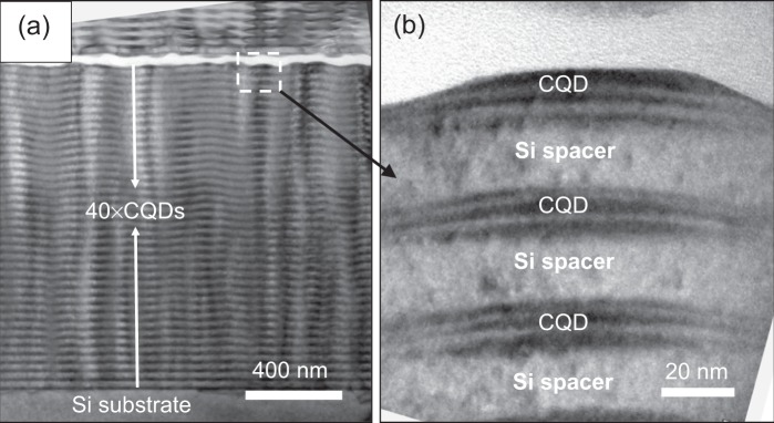
A further sample set was a series of multifold Ge/Si/Ge stacked structures (CQDs) with varying thermoelectric functionality, which is due to different thicknesses of inserted Si and numbers of Ge stacks. They were CVD grown on p-type (001)-oriented Si wafers (10–25 Ω × cm), 150 mm in diameter, with ≈0.15 nm thick insulating layer of SiO2, which was used to electrically isolate the stacks from the substrate. The growth temperature was set at 600 °C. Further details on the structure growth system can be found elsewhere20,21. Here, two sets of samples were compared, which are referred to as 2-fold and 3-fold CQDs. The 2-fold CQDs consists of the sequence of Ge (12.6 MLs)/Si (2 nm)/Ge (12.6 MLs) layers, whereas the Ge (12.6 MLs)/Si (2 nm)/Ge (12.6 MLs)/Si (2 nm)/Ge (12.6 MLs) sequence was developed in 3-fold CQDs. As shown in Fig. 2(a), 40-period multifold CQDs were grown to build up a thin-film-like material, ~1.5 μm thick, for thermoelectric measurements. Each multifold CQD layer was separated by 20 nm Si spacer layers.
Figure 2.
XTEM micrograph of a 3-fold coupled QD structure (40 periods of CQD/Si stacks) (a). A magnified image of the dashed rectangular region in (a) for three selected CQDs near the top stack is shown in (b). Each CDQ is composed of Ge layers (three distinct dark regions shown in the right-hand image), whereas the two white areas corresponding to Si layers are inserted into the dot. Higher resolution image of CDQs is given in Supplementary Fig. S2.
Although non intentionally doped, those CQD fllms revealed n-type behavior with a room-temperature resistivity of about 0.09 Ω × cm, which corresponds to concentrations of ≈1 × 1017 cm−3. This may be due to the fact that type II Ge/Si heterostructure forms the potential well for holes in the valence band of GexSi1−x inclusions38. Our theoretical estimates gave the resulting electron concentration of ≈0.5 × 1017 cm−3 in the CQD fllms, which is fairly close to the measured value.
The Seebeck coefficient was measured using the general approach reviewed by Martin et al.39. Our automatic home-built measuring system is schematically sketched in Fig. 3. Because of flow of current through the heater with a resistance R (1 in Fig. 3) mounted on the sample the temperature rises at the heater side of the sample. A thermal bath at the opposite sample side works as a temperature-controlled heat sink (Fig. 3). In turn, a local temperature difference ΔT = T2 − T3 is built up between temperature-sensing diodes 2 and 3, and the thermoelectric voltage ΔV is measured between contacts 4 and 5. The temperature sensors were calibrated before Seebeck measurement. A closed-cycle cryostat (CS204, Advanced Research Systems) was used to vary the temperature of the sample.
Figure 3.
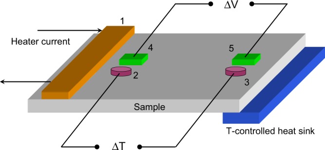
A schematic diagram for the Seebeck coefficient measurement. 1 - heater (100-Ω SMD resistor), 2 and 3 - temperature sensors (BAP64-02NXP diodes), 4 and 5 - metal pads (InGa), which form Ohmic contacts to the semiconductor. Heat is extracted by channeling it into the cold head of the cryostat connected directly to the sample edge (T-controlled heat sink).
In our experimental setup, the heater current IR is determined by measuring an applied voltage, which varies as square root of time. In this case, both the electrical power IR2R and the temperatures sensed by diodes 2 and 3 increase with a linear dependence on time. This behaviour is exemplified in Fig. 4(a). At time t = 0, the controller of the cryostat temperature is set to a 5° larger temperature value, so the diode readings evolve in time, as shown by curves 2 and 3 in Fig. 4(a). Well after the readings saturate and the temperature is stabilized at the larger value of T (horizontal part of curves 2 and 3 at t ≥ 40 s in Fig. 4(a)) the heating is applied to the heater 1 in Fig. 3 at t = 90 s (arrow “Heat” in Fig. 4(a)).
Figure 4.
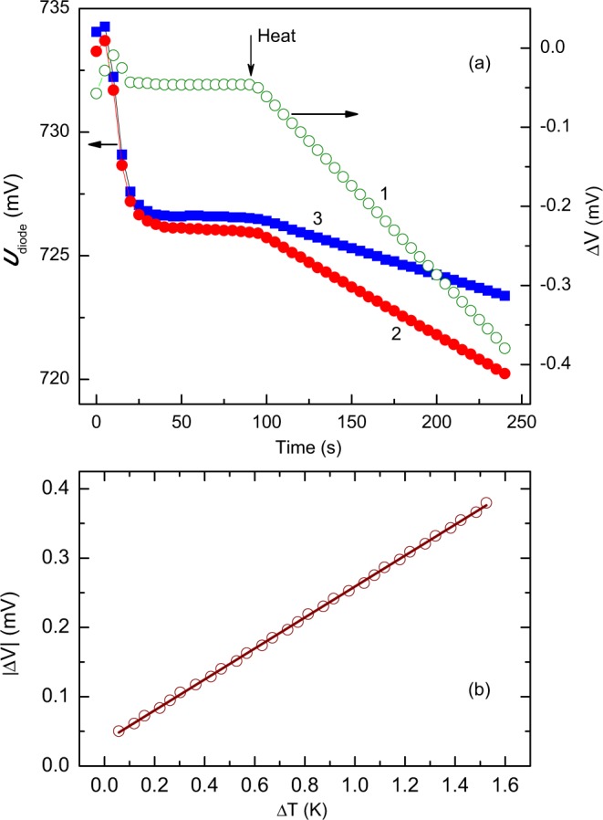
(a) Real-time monitoring of the temperature-sensing diode voltages (curves 2 and 3 correspond to diodes 2 and 3 in Fig. 3) after the cryostat temperature controller is set to 5° temperature increase at t = 0 and after the heater 1 in Fig. 3 is energised at t = 90 s. The diode voltages and ΔV (curve 1) are read with a 16 bit analog-to-digital converter (Analog Devices AD7792). (b) Voltage monitoring during Seebeck coefficient measurements in regular-QD sample at T = 243 K. Circles - experimental data. Line is a linear fit to the data yielding S = 0.223 mV/K.
When current is applied through the heater (1 in Fig. 3), there is a temperature rise behind the heater area, which yields the temperature difference ΔT between the sensors (2 and 3) sitting on the sample surface. Hence, curves 2 and 3 in Fig. 4(a) gradually diverge at time instants greater than that marked by arrow “Heat”. The resulting temperature difference ΔT increasing in time creates a thermoelectric voltage ΔV (curve 1 in Fig. 4(a)), which responses to the changes in ΔT. Figure 4(b) shows the linear fit to the measured ΔV vs ΔT data, which has a slope of 0.223 mV/K equal to the value of the Seebeck coefficient.
Further experimental details are given below in Methods section.
Results and Discussion
Raman spectra of our samples are shown in Fig. 5. Three GexSi1−x alloy phonon modes are clearly seen, which correspond to Ge-Ge (at frequency ω1), Si-Ge (ω2) and Si-Si vibrations. It is known that the frequencies of the Ge-Ge and Si-Ge modes vary with the Ge fraction x and in-plane strain 〈S∥〉 as follows40:
| 1 |
| 2 |
Figure 5.
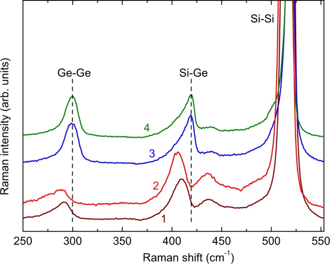
Raman spectra of samples L (1) and MDL (2), 2-fold (3) and 3-fold (4) coupled QD structures. Two dashed lines are used to guide the eye to show the different frequencies of the Ge-Ge and Si-Ge modes.
where b1 and b2 are the phonon strain-shift coefficients for the Ge-Ge and Si-Ge modes, respectively. In order to obtain an estimate of the x and 〈S∥〉 values, we use b1 = −400 cm−1 and b2 = −575 cm−1 given by Tan et al.41 and Lin et al.42. The calculated values for these parameters are given in Table 1.
Table 1.
The Ge-Ge and Si-Ge Raman frequencies obtained from spectra in Fig. 5 and the values of x and 〈S∥〉 calculated using Eqs 1 and 2.
| Sample | ω1 (cm−1) | ω2 (cm−1) | x | 〈S∥〉 (%) |
|---|---|---|---|---|
| L | 291.7 | 410.3 | 0.34 | −0.008 |
| MDL | 288.2 | 406.3 | 0.25 | −0.003 |
| 2-fold CQDs | 299.2 | 418.7 | 0.54 | −0.020 |
| 3-fold CQDs | 299.8 | 419.1 | 0.57 | −0.021 |
It is seen that the concentration of Ge atoms in the CQDs layers is about 55%, showing that intermixing of Si and Ge occurs during the growth process, which is a common process in crystallization of Si/Ge multilayers43,44. It is also seen in Table 1 that in both 2-fold and 3-fold CQDs layers the values of x are very close to each other.
In order to decipher how the QD structure evolves during this process and provide supporting evidence for the intermixing, we performed a numerical study based on molecular dynamics (see Supplementary Video). From this simulation, the value x = 0.67 was obtained, which is in reasonable overall agreement with that obtained in Raman experiments.
The measured temperature dependencies of the Seebeck coefficient for different samples are shown by the data points in Fig. 6. These data indicate that S drops with decreasing electrical resistivities of our samples (≈0.09 Ω × cm in CQDs, 0.04 Ω × cm in MDL, 0.03 Ω × cm in L), which follows the trend established in Fig. 1.
Figure 6.
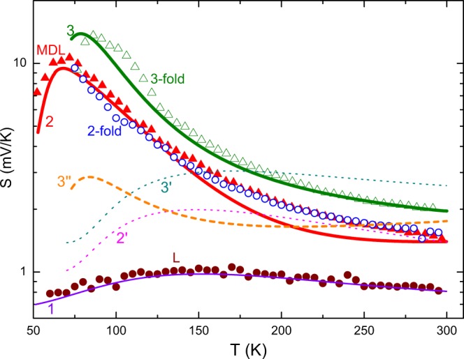
Temperature dependence of S for samples L, MDL, 2-fold and 3-fold coupled QD structures studied experimentally (data points) and theoretically (lines).
As stated in the Introduction, computations can be based on the Boltzmann transport equation. The comparison between experimental data of Fig. 6 and model predictions was carried out considering the contribution of the diffusive Sd and phonon drag Sp components into the Seebeck coefficient S. Based on the preceding literature survey, we employ the general calculation framework addressed by Mahan et al.45. The carrier diffusion term in n-type layers is
| 3 |
Similarly for p-type layers
| 4 |
where e is the electron charge, Ec is the conduction band minimum, Eg is the band gap, μ = μ(T) is the Fermi level, kB is the Boltzman constant and the ratio I1/I2 is taken in the integral forms
where the variable is the dimensionless energy of the carrier with the wave vector and lifetime τ(ξ).
In sample L, we consider a uniformly doped single layer of Ge 0.34Si 0.66 and combine relevant scattering mechanisms to get total phonon (τp) and electron (τe) lifetimes. These can be numerically calculated in the framework described, for example, by Ziman46. Here, we include phonon-phonon normal and Umklapp processes, alloy scattering and boundary scattering of phonons at the inner boundaries for calculating τp. The computed τe value takes into account different scattering centers such as impurities and phonons. These scattering mechanisms were combined using the Matthiessen’s rule.
The phonon lifetime τp is calculated by following a procedure given by Mahan et al.45. In our fitting, input parameters for silicon (not SiGe) are used, which are taken from ref. 45. To account for GexSi1−x alloy, we replace isotope scattering by alloy scattering in GexSi1−x with the value of x taken from Table 1. The electron lifetime τe is obtained for GexSi1−x using the approach and input parameters described by Yi and Yu47. The model we use here also involves a set of additional physical parameters which are taken from the literature45,47. The solid line 1 in Fig. 6 represents the fitting result in sample L, exhibiting an excellent agreement with measurement data given by closed circles.
However, this approach cannot be straightforwardly applied to MDL and CQD samples, as illustrated by curves 2′ and 3′ in Fig. 6. It is seen that similarly modeled S(T) curves to include τp and τe exhibit a noticeable discrepancy between the expected (curves 2′ and 4′) and measured (closed and open triangles in Fig. 6, respectively) values of S. Based on the experimental results given in the Introduction, we may therefore conclude that in our MDL and CQD samples enhancement of the phonon scattering due to inner boundaries in the GexSi1−x layer and Ge/Si/Ge stacks has to be taken into account.
Speaking qualitatively, the phonons preferentially move from the hot to cold sample side in the temperature gradient across them. This in turn forces the carriers to move in the same direction and this effect is gradually quenched with increasing T due to anharmonic interatomic forces48. This would increase S at low temperatures, as indeed observed in our S(T) experiments. It is seen in Fig. 6 that this rise in S is most pronounced in MDL and CQD samples (open circles and triangles). The decrease in S with further decreasing temperature can naturally be explained by the contribution of the boundary scattering of phonons48,49. As expected, increasing the number of embedded scatterers would make this effect more marked, which is also observed in Fig. 6 (open triangles compared with open circles).
Therefore, following the procedure described above, we now consider two more relaxation processes for modeling S(T) curves in MDL and CQD samples, which involve the scattering from the inner interfaces in τp and the carrier filtering in τe. In both samples, the boundary scattering is taken into account when calculating the phonon drag term as
| 5 |
where d is the distance between boundaries and interfaces that scatter incident phonons (see Fig. 7), Da is the deformation potential parameter, is the Planck constant, θD is the Debye temperature, ρ0 is the sample density, aB is the effective Bohr radius of the impurity, Ei is the binding energy of the impurity and
where υL and υT are the speeds of the longitudinal and transverse acoustic waves, respectively, y = qaB is the phonon integration variable, q is the phonon wave number, g2 is the coupling coefficient for isotope scattering and Ω0 is the unit cell volume. The interface specularity parameter α is included in the first term of the phonon scattering rate τp−1(y) as discussed elsewhere47. For the specular reflection α = 1, and for the totally diffusive scattering of phonons α = 0. Values of δ (ranging from 1.4 to 2.3) and τp0 were found to be very temperature dependent45.
Figure 7.
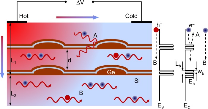
Schematics of phonon scattering processes from the 2-fold CQD inclusions (A) and the phonon drag (B) contribution to the thermoelectric voltage ΔV. Electron and hole are indicated by a circle and labeled e− and h+, respectively. Horizontal and vertical arrows illustrate a heat flux from hot to cold parts of the sample. L1 and L2 indicate the thickness of the quantum dot and buffer Si layers, respectively. In our CQD samples, L2 = 50 nm and L1 ≈ 1.4 μm in 2-fold and 1.8 μm in 3-fold CQD structures. Computationally, a one-dimensional unit cell spans the buffer Si layer (L2) and 4 periods of CQD layers (L1 = 140 nm in 2-fold and 180 nm in 3-fold CQDs). Lb and wb indicates the fitting parameters of the barriers generated by embedded CQDs (see Supplementary Fig. S4). High-energy electrons move above the energy barrier (process B on the right-hand side) while the ones with energies less than the barrier height are scattered back (process A). Conduction- and valence-band edges are marked as Ec and Ev, respectively.
For handling the total Seebeck coefficient, we artificially divide each layer d in Fig. 7 into a certain number N of sublayers having a thickness of di (i = 1,2, ..., N). We choose here the thickness of the sublayer varying from 15 to 25 nm. Following a calculation similar to that of Bahk et al.50, the total measured value of S is the weighted averaging of the mN values developed in the sublayers with m being the number of repeated layers (d in Fig. 7) in the sample. The weights are written in proportion to the electrical conductivity σi of the i-th sublayer multiplied by the thickness di as
| 6 |
where the subscript i denotes the constituent Sd and Sp coefficients for the i-th sublayer. The electrical conductivity is defined47 by
| 7 |
where m* is the effective mass of the carrier and τi is the total lifetime in the i-th sublayer. Using Matthiessen’s rule, τi was obtained from the lifetimes due to different scattering mechanisms discussed above.
The specularity parameter α and the value of τp0 in the phonon scattering rate τp−1(y) were adjusted to match the S(T) data from the experiment. Solid line 2 in Fig. 6 is the best-fit curve to the filled triangular experimental data points for sample MDL. It is seen that curve 2 gives a good fit at temperatures below ≈150 K and at about T = 300 K. The model accounting for the interface scattering (curve 2 in Fig. 6) produces much better agreement with the experimental data for temperatures ≤175 K than the model yielding curve 2′.
This is in marked contrast to what one observes for multifold Ge/Si/Ge CQD structures. Indeed, dashed line 3″ in Fig. 6, computed similar to curve 2 for MDL sample, shows discrepancy to the experimental values (open triangles), which are too large at low temperatures and are somewhat smaller at temperatures greater than ≈200 K. We, therefore, have considered a subsidiary contribution of the carrier filtering to explain the experimental data for CQDs shown by open circles and triangles in Fig. 6. These calculations show that the S(T) data obtained in our experiments can be properly modeled by filtering the carriers with energies less than the barrier height.
Here we use the schematics of the scattering and filtering effects described by Zhou et al.30. Schematic illustration of the interaction between phonons and CQD inclusions and phonon drag processes is shown in Fig. 7 by arrows A and B, respectively. The quantum dot layer with thickness L1 and thin buffer layer (L2), which are included into our calculation unit cell, are depicted in Fig. 7. In the type II SiGe/Si heterostructure, the band edge discontinuities have different signs for the conduction and valence bands51, as indicated in the right-hand side of Fig. 7. The interaction of electrons with CQDs (process A in Fig. 7) is modeled by the relaxation time τbi, which is approximated by the interface scattering in the i-th sublayer. If the average energy of moving electrons is less than the barrier height Eb, they bounce back from the barrier (A in the right-hand side of Fig. 7). If the energy of electrons or holes exceeds the barrier height Eb, they pass through the boundary region, as shown by processes B in Fig. 7.
The quantity τbi = λi/υi, where is the average velocity of the carriers with energy εi and λi is their mean-free paths52
| 8 |
with T(εi) the transmission probability for the carriers through a barrier.
We find that this method provides an adequate fit to the experimental S(T) data in CQD samples using only Lb and wb as slightly adjustable parameters (aside from the ones used to fit the data in sample MDL). The model fit to the temperature-dependent Seebeck coefficient of 3-fold CQDs is shown by solid line 3 in Fig. 6. In all the temperature range, the agreement between the experimental values and those found from the fit to S(T) is excellent. In the case of 2-fold CQDs (open circles in Fig. 6), the discussed scattering effects are capable to consistently explain the experimental results, so that the the measured Seebeck coefficient and its temperature dependence can be fitted quite well by the computed curve (not shown in Fig. 6).
The values of the parameters used to generate the fits are Lb = 90 nm (3-fold CQDs), 100 nm (2-fold CQDs), wb = 40 nm (3-fold CQDs), 60 nm (2-fold CQDs), α = 1.2 × 10⁻² (3-fold CQDs), 2.3 × 10⁻² (2-fold CQDs) and Eb = 0.37 eV in both samples (see Supplementary Fig. S4). Perhaps the most interesting result is that the specularity parameter α in 2-fold CQDs is roughly two times greater than the appropriate value observed in 3-fold CQDs, indicative of the fact that the interface is seen more rough in the latter sample with increased number of Si layers inserted into the quantum dot. It is most remarkable that the Seebeck coefficient corresponding to different CQD samples concomitantly increases with increasing the number of the inserted layers. Because the only difference between the 2-fold and 3-fold CQD samples is the one more Si layer inserted into the 3-fold quantum dot that leads to enhanced interface scattering of phonons, which, in turn, increases S. It is seen in Fig. 6 that the experimental S(T) data corresponding to the two CQD samples are nearly parallel to each other above ≈80 K (open circles and triangles), exhibiting increase in S of about 40% due to additional Si layer inserted into the dot.
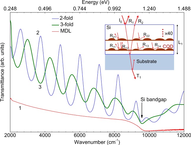
Another test of this type, estimating the degree to which the interface scattering effects can be modified using composite quantum dots, is shown in Fig. 8. In this figure we plot the infrared (IR) transmittance spectra for MDL and CQD samples. In this experiment, the sample is illuminated from the front with an intensity of the incident light of I0 (inset in Fig. 8). The incident radiation is in part reflected at the layer top and bottom surfaces, as indicated by arrows R1 and R2, respectively, and transmitted through the sample (T1). Clear Fabry-Perot oscillations are observed in spectra 2 and 3 in Fig. 8 due to the interference between the partially reflected IR beams R1 and R2 shown in the inset of Fig. 8. However, these oscillations are not observable in sample MDL (spectrum 1 in Fig. 8). This is clearly in accord with the fact that the oscillations can occur if the layer thickness is comparable with the light wavelength due to the coherent multiple reflections53.
Figure 8.
Room temperature IR transmittance spectra of sample MDL (1), 2-fold (2) and 3-fold (3) CQD structures. Inset: Ray diagram of the incident light (I0) within a CQD sample with the reflection from the front and rear surfaces and various interfaces. R11, R12, ..., R22 illustrate reflectivities from the inner boundaries.
The second factor of observing the oscillations is a high enough optical transparency of the layered structure. This transparency is apparently affected by the presence of CQD scatterers between the two reflecting surfaces formed by the top and bottom interfaces of the deposited layer. Diffuse scattering of the light beam, which is highlighted by arrows R11, R12, …, R22 in the inset of Fig. 8, weakens the interference signals. Therefore, the amplitude of the transmitted light drops off very rapidly as the roughness of the inner interfaces is raised, as derived by Kan et al.54. Strictly speaking, specularity of an interface to an incident wave depends on the radiation wavelength relative to the roughness height and correlation length, as has been mentioned by Ogilvy55. Therefore, the scattering of electromagnetic and lattice waves should generally not be compared with each other. Meanwhile, it is remarkable that the quenching of the interference fringes observed in spectrum 3 of Fig. 8 compared with spectrum 2 and the increased S in 3-fold CQDs compared with that in 2-fold CQDs (open triangles and open circles in Fig. 6, respectively) both give a good indication of the increased interface roughness in 3-fold CQDs.
In conclusion, we have combined experiment and theory to deliver the first direct evidence that placing thin silicon layers inside the germanium quantum dot (multi-fold CQD material) can offer considerable enhancement of the Seebeck effect. We show that the Seebeck coefficient gets enhanced up to ≈40% in the 3-fold CQD material compared with the 2-fold CQDs. We present a numerical model to faithfully account for this enhancement, which relates the enlarged Seebeck coefficient to efficient scattering of phonons by inner boundaries and the carrier filtering by the CQD inclusions. These composite Ge/Si composite quantum dots can be competitive for the applications related to on-chip temperature control through micro-refrigeration and autonomous renewable energy systems. Moreover, we anticipate that the phonon scattering techniques developed here could significantly augment the thermoelectric performance of Ge/Si materials through further optimization of the layer stacks inside the quantum dot and of the dopant concentrations.
Methods
Sample characterization
Cross-sections of the microstructures were observed on a JEOL JEM-2100 transmission electron microscope (XTEM) operating at 200 kV. Raman spectra measurements were performed at room temperature with a 514.5-nm line of an Ar+ laser using a Horiba Jobin-Yvon T64000 spectrometer. The laser light was focused onto the sample surface to a spot of 0.7 μm in diameter using Olympus objective (50×, NA = 0.5). Raman measurements were performed in the z(x, y) scattering geometry, where x, y, and z correspond to the crystallographic directions [100], [010], and [001] of Si, respectively. This Raman geometry is allowed for scattering by LO phonons in Ge and Si and forbidden for two-phonon scattering by TA phonons of Si substrate, which thus allowed to avoid complications in the interpretation of Raman spectra56. Room temperature transmission FTIR spectra in the 2000–12000 cm−1 wavenumber range were obtained at normal incidence using Bruker Vertex 70V FTIR spectrometer with a Globar source. For each spectrum, 64 scans were averaged with a spectral resolution of 1 cm−1. The layer resistance was measured employing the transmission line measurement technique57.
Simulations
Numerical analysis of the integrals I1, I2 and I3 in Eqs (3), (4) and (5) was performed using the extended trapezoidal rule and the Fortran code available on pp. 1052–1056 in the book of Press et al.58. Supplementary Video clip was created using the open visualization tool OVITO. The program is freely available under an open source license at https://ovito.org.
Supplementary information
Acknowledgements
This work was partially supported by the National Nano Device Laboratories and National Science Council of Taiwan under Contracts no. NSC-100-2221-E-008-016-MY3 and NSC-103-2221-E-008-116-MY3.
Author contributions
S.-W.L. and P.-W.L. fabricated the CQD structures and performed electron microscopy measurements. O.K. and A.N. contributed to the design of SiGe layers and execution of the experiment, V.S. designed the study of the SiGe composition and performed optical measurements, V.K. performed the calculations, O.K., P.-W.L. and S.-W.L. analysed the data and co-wrote the paper. All authors discussed the results and commented on the manuscript.
Competing interests
The authors declare no competing interests.
Footnotes
Publisher’s note Springer Nature remains neutral with regard to jurisdictional claims in published maps and institutional affiliations.
Supplementary information
is available for this paper at 10.1038/s41598-019-52654-z.
References
- 1.Simons, R. E., Antonetti, V. W., Nakayama, W. & Oktay, S. Heat Transfer in Electronic Packages in Microelectronics Packaging Handbook, Vol. 1, Chap. 4, p. 314 (Chapman and Hall, New York, 1997).
- 2.Alam H, Ramakrishna S. A review on the enhancement of figure of merit from bulk to nano-thermoelectric materials. Nano Energy. 2013;2:190–212. doi: 10.1016/j.nanoen.2012.10.005. [DOI] [Google Scholar]
- 3.Shakouri A, Zhang Y. On-chip solid-state cooling for integrated circuits using thin-film microrefrigerators. IEEE Trans. Components Packag. Technol. 2005;28:65–69. doi: 10.1109/TCAPT.2005.843219. [DOI] [Google Scholar]
- 4.Dresselhaus MS, et al. New directions for low-dimensional thermoelectric materials. Adv. Mater. 2007;19:1043–1053. doi: 10.1002/adma.200600527. [DOI] [Google Scholar]
- 5.Nishibori M, et al. Thermoelectric hydrogen sensors using Si and SiGe thin films with a catalytic combustor. J. Ceramic Soc. Jap. 2006;118:188–192. doi: 10.2109/jcersj2.118.188. [DOI] [Google Scholar]
- 6.Pichanusakorn P, Bandaru P. Nanostructured thermoelectrics. Mater. Sci. Eng. R. 2010;67:19–63. doi: 10.1016/j.mser.2009.10.001. [DOI] [Google Scholar]
- 7.Vineis CJ, Shakouri A, Majumdar A, Kanatzidis MG. Nanostructured thermoelectrics: big efficiency gains from small features. Adv. Mater. 2010;22:3970–3980. doi: 10.1002/adma.201000839. [DOI] [PubMed] [Google Scholar]
- 8.Gayner C, Kar KK. Recent advances in thermoelectric materials. Progr. Mater. Sci. 2016;83:330–382. doi: 10.1016/j.pmatsci.2016.07.002. [DOI] [Google Scholar]
- 9.Choi H, et al. Enhancement in thermoelectric properties of Te-embedded Bi2Te3 by preferential phonon scattering in heterostructure interface. Nano Energy. 2018;47:374–384. doi: 10.1016/j.nanoen.2018.03.009. [DOI] [Google Scholar]
- 10.Ahmad S, et al. Enhanced thermoelectric figure-of-merit of p-type SiGe through TiO2 nanoinclusions and modulation doping of boron. Materialia. 2018;4:147–156. doi: 10.1016/j.mtla.2018.09.029. [DOI] [Google Scholar]
- 11.Zardo I, Rurali R. Manipulating phonons at the nanoscale: impurities and reduced dimensionality. Curr. Opin. Green Sustain. Chem. 2019;17:1–7. doi: 10.1016/j.cogsc.2018.12.006. [DOI] [Google Scholar]
- 12.Mao J, Wang Y, Liu Z, Ge B, Ren Z. Phonon scattering by nanoscale twin boundaries. Nano Energy. 2017;32:174–179. doi: 10.1016/j.nanoen.2016.12.026. [DOI] [Google Scholar]
- 13.Zhao L, He Y, Zhang H, Yi L, Wu J. Enhancing the thermoelectric property of Bi2Te3 through a facile design of interfacial phonon scattering. J. Alloys Compd. 2018;768:659–666. doi: 10.1016/j.jallcom.2018.07.324. [DOI] [Google Scholar]
- 14.Yadav S, Chaudhary S, Pandya DK. Incorporation of MoS2 nanosheets in CoSb3 matrix as an efficient novel strategy to enhance its thermoelectric performance. Appl. Surf. Sci. 2018;435:1265–1272. doi: 10.1016/j.apsusc.2017.11.262. [DOI] [Google Scholar]
- 15.Sakane S, et al. Thermoelectric power factor enhancement based on carrier transport physics in ultimately phonon-controlled Si nanostructures. Mater. Today Energy. 2019;13:56–63. doi: 10.1016/j.mtener.2019.04.014. [DOI] [Google Scholar]
- 16.Liang X, Shen L, Wang C. Origin of anisotropy and compositional dependence of phonon and electron transport in ZnO based natural superlattices and role of atomic layer interfaces. Nano Energy. 2019;59:651–666. doi: 10.1016/j.nanoen.2019.03.007. [DOI] [Google Scholar]
- 17.Kim C, Baek JY, Lopez DH, Kim DH, Kim H. Interfacial energy band and phonon scattering effect in Bi2Te3-polypyrrole hybrid thermoelectric material. Appl. Phys. Lett. 2018;113:153901. doi: 10.1063/1.5050089. [DOI] [Google Scholar]
- 18.Tureson N, et al. Effect of ion-implantation-induced defects and Mg dopants on the thermoelectric properties of ScN. Phys. Rev. B. 2018;98:205307. doi: 10.1103/PhysRevB.98.205307. [DOI] [Google Scholar]
- 19.Tayari V, et al. Quasi-two-dimensional thermoelectricity in SnSe. Phys. Rev. B. 2018;97:045424. doi: 10.1103/PhysRevB.97.045424. [DOI] [Google Scholar]
- 20.Chang H-T, Wang S-Y, Lee S-W. Designer Ge/Si composite quantum dots with enhanced thermoelectric properties. Nanoscale. 2014;6:3593–3598. doi: 10.1039/C3NR06335F. [DOI] [PubMed] [Google Scholar]
- 21.Chang H-T, et al. High quality multifold Ge/Si/Ge composite quantum dots for thermoelectric materials. Appl. Phys. Lett. 2013;102:101902. doi: 10.1063/1.4794943. [DOI] [Google Scholar]
- 22.Wood C. Materials for thermoelectric energy conversion. Rep. Progr. Phys. 1988;51:459–539. doi: 10.1088/0034-4885/51/4/001. [DOI] [Google Scholar]
- 23.Wu MW, Horing NJM, Cui HL. Phonon-drag effects on thermoelectric power. Phys. Rev. B. 1996;54:5438–5443. doi: 10.1103/PhysRevB.54.5438. [DOI] [PubMed] [Google Scholar]
- 24.Zianni X, Butcher PN, Kearney MJ. Semiclassical magnetothermopower of a quasi-tvvo-dimensional electron gas. Phys. Rev. B. 1994;49:7520–7527. doi: 10.1103/PhysRevB.49.7520. [DOI] [PubMed] [Google Scholar]
- 25.Boukai AI, et al. Silicon nanowires as efficient thermoelectric materials. Nature. 2008;451:168–171. doi: 10.1038/nature06458. [DOI] [PubMed] [Google Scholar]
- 26.Weber L, Gmelin E. Transport properties of silicon. Appl. Phys. A. 1991;53:136–140. doi: 10.1007/BF00323873. [DOI] [Google Scholar]
- 27.Nanoscale Thermoelectrics (eds Wang, X. & Wang, Z. M.) (Springer, 2014).
- 28.Conwell EM, Zucker J. “Thermoelectric effect” of hot carriers. J. Appl. Phys. 1965;36:2192–2196. doi: 10.1063/1.1714448. [DOI] [Google Scholar]
- 29.Harman T, Taylor P, Walsh M, LaForge B. Quantum dot superlattice thermoelectric materials and devices. Science. 2002;297:2229–2232. doi: 10.1126/science.1072886. [DOI] [PubMed] [Google Scholar]
- 30.Zhou J, Li X, Chen G, Yang R. Semiclassical model for thermoelectric transport in nanocomposites. Phys. Rev. B. 2010;82:115308. doi: 10.1103/PhysRevB.82.115308. [DOI] [Google Scholar]
- 31.Xiao Y, et al. Synergistic tuning of carrier and phonon scattering for high performance of n-type Bi2Te2.5Se0.5 thermoelectric material. J. Mater. Chem. A. 2015;3:22332–22338. doi: 10.1039/C5TA06107E. [DOI] [Google Scholar]
- 32.Vargiamidis V, Thesberg M, Neophytou N. Theoretical model for the Seebeck coefficient in superlattice materials with energy relaxation. J. Appl. Phys. 2019;126:055105. doi: 10.1063/1.5108607. [DOI] [Google Scholar]
- 33.Vargiamidis V, Neophytou N. Hierarchical nanostructuring approaches for thermoelectric materials with high power factors. Phys. Rev. B. 2019;99:045405. doi: 10.1103/PhysRevB.99.045405. [DOI] [Google Scholar]
- 34.Ohnishi M, Shiomi J. Towards ultimate impedance of phonon transport by nanostructure interface. Appl. Phys. Lett. Mater. 2019;7:013102. [Google Scholar]
- 35.Fiorentini V, Farris R, Argiolas E, Maccioni MB. High thermoelectric figure of merit and thermopower in layered perovskite oxides. Phys. Rev. Mater. 2019;3:022401. doi: 10.1103/PhysRevMaterials.3.022401. [DOI] [Google Scholar]
- 36.Gelda D, et al. Specularity of longitudinal acoustic phonons at rough surfaces. Phys. Rev. B. 2018;97:045429. doi: 10.1103/PhysRevB.97.045429. [DOI] [Google Scholar]
- 37.Murota J, Sakuraba M, Tillack B. Atomically controlled processing for group IV semiconductors by chemical vapor deposition. Jpn. J. Appl. Phys. 2006;45:6767–6785. doi: 10.1143/JJAP.45.6767. [DOI] [Google Scholar]
- 38.Brunner K. Si/Ge nanostructures. Rep. Prog. Phys. 2002;65:27–72. doi: 10.1088/0034-4885/65/1/202. [DOI] [Google Scholar]
- 39.Martin J, Tritt T, Uher C. High temperature Seebeck coefficient metrology. J. Appl. Phys. 2010;108:121101. doi: 10.1063/1.3503505. [DOI] [Google Scholar]
- 40.Alonso MI, de la Calle M, Ossó JO, Garriga M, Goñi AR. Strain and composition profiles of self-assembled Ge/Si(001) islands. J. Appl. Phys. 2005;98:033530. doi: 10.1063/1.2006229. [DOI] [Google Scholar]
- 41.Tan PH, Brunner K, Bougeard D, Abstreiter G. Raman characterization of strain and composition in small-sized self-assembled Si/Ge dots. Phys. Rev. B. 2003;68:125302. doi: 10.1103/PhysRevB.68.125302. [DOI] [Google Scholar]
- 42.Lin JH, et al. Strain analysis of Ge/Si(001) islands after initial Si capping by Raman spectroscopy. J. Appl. Phys. 2007;101:083528. doi: 10.1063/1.2721875. [DOI] [Google Scholar]
- 43.Czigány Z, Radnóczi G, Järrendahl K, Sundgren J-E. Annealing induced interdiffusion and crystallization in sputtered amorphous Si/Ge multilayers. J. Mater. Res. 1997;12:2255–2261. doi: 10.1557/JMR.1997.0301. [DOI] [Google Scholar]
- 44.Lee SW, et al. Self-assembled nanorings in Si-capped Ge quantum dots on (001)Si. Appl. Phys. Lett. 2003;83:5283–5285. doi: 10.1063/1.1635073. [DOI] [Google Scholar]
- 45.Mahan GD, Lindsay L, Broido DA. The Seebeck coefficient and phonon drag in silicon. J. Appl. Phys. 2014;116:245102. doi: 10.1063/1.4904925. [DOI] [Google Scholar]
- 46.Ziman, J. M. Electrons and Phonons (Clarendon, Oxford, 2001).
- 47.Yi S, Yu C. Modeling of thermoelectric properties of SiGe alloy nanowires and estimation of the best design parameters for high figure-of-merits. J. Appl. Phys. 2015;117:035105. doi: 10.1063/1.4906226. [DOI] [Google Scholar]
- 48.Herring C. Theory of the thermoelectric power of semiconductors. Phys. Rev. 1954;96:1163–1187. doi: 10.1103/PhysRev.96.1163. [DOI] [Google Scholar]
- 49.Pokharel M, et al. Phonon drag effect in nanocomposite FeSb2. MRS Commun. 2013;3:31–38. doi: 10.1557/mrc.2013.7. [DOI] [Google Scholar]
- 50.Bahk JH, Favaloro T, Shakouri A. Thin film thermoelectric characterization techniques. Annu. Rev. Heat Transfer. 2013;16:51–99. doi: 10.1615/AnnualRevHeatTransfer.v16.30. [DOI] [Google Scholar]
- 51.Brennan, K. F. & Brown, A. S. Theory of Modern Electronic Semiconductor Devices (Wiley, New York, 2002).
- 52.Popescu A, Woods LM, Martin J, Nolas GS. Model of transport properties of thermoelectric nanocomposite materials. Phys. Rev. B. 2009;79:205302. doi: 10.1103/PhysRevB.79.205302. [DOI] [Google Scholar]
- 53.Katsidis CC, Siapkas DI. General transfer-matrix method for optical multilayer systems with coherent, partially coherent, and incoherent interference. Appl. Opt. 2002;41:3978–3987. doi: 10.1364/AO.41.003978. [DOI] [PubMed] [Google Scholar]
- 54.Kan PYY, Foss SE, Finstad TG. The effect of etching with glycerol, and the interferometric measurements on the interface roughness of porous silicon. Phys. Stat. Sol. (a) 2005;202:1533–1538. doi: 10.1002/pssa.200461173. [DOI] [Google Scholar]
- 55.Ogilvy JA. Wave scattering from rough surfaces. Rep. Prog. Phys. 1987;50:1553–1608. doi: 10.1088/0034-4885/50/12/001. [DOI] [Google Scholar]
- 56.Baranov AV, Fedorov AV, Perova TS. Analysis of strain and intermixing in single-layer Ge/Si quantum dots using polarized Raman spectroscopy. Phys. Rev. B. 2006;73:075322. doi: 10.1103/PhysRevB.73.075322. [DOI] [Google Scholar]
- 57.Berger HH. Models for contacts to planar devices. Sol. State Electron. 1972;15:145–158. doi: 10.1016/0038-1101(72)90048-2. [DOI] [Google Scholar]
- 58.Press, W. H., Teukolsky, S. A., Vetterling, W. T. & Flannery, B. P. Numerical recipes in Fortran 90. The art of parallel scientific computing Vol. 2 (Cambridge University Press, New York, 1996).
- 59.Morelli DT, Heremans JP, Slack GA. Estimation of the isotope effect on the lattice thermal conductivity of group IV and group III-V semiconductors. Phys. Rev. B. 2002;66:195304. doi: 10.1103/PhysRevB.66.195304. [DOI] [Google Scholar]
Associated Data
This section collects any data citations, data availability statements, or supplementary materials included in this article.


