Abstract
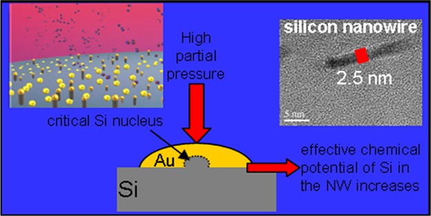
Quantum confinement effects in silicon nanowires (SiNWs) are expected when their diameter is less than the size of the free exciton (with a Bohr radius ∼5 nm) in bulk silicon. However, their synthesis represents a considerable technological challenge. The vapor–liquid–solid (VLS) mechanism, mediated by metallic nanoclusters brought to the eutectic liquid state, is most widely used for its simplicity and control on the SiNWs size, shape, orientation, density, and surface smoothness. VLS growth is often performed within high-vacuum physical vapor deposition systems, where the eutectic composition and the pressure conditions define the minimum diameter of the final nanowire usually around 100 nm. In this article, we present and discuss the SiNWs’ growth by the VLS method in a plasma-based chemical vapor deposition system, working in the mTorr pressure range. The purpose is to demonstrate that it is possible to obtain nanostructures with sizes well beyond the observed limit by modulating the deposition parameters, like chamber pressure and plasma power, to find the proper thermodynamic conditions for nucleation. The formation of SiNWs with sub-5 nm diameter is demonstrated.
Introduction
One-dimensional (1D) semiconductor nanostructures exhibit extraordinary electronic, optical, chemical, mechanical, and thermal properties, and for these reasons they have applications in very different areas such as electronics, sensors, optoelectronics, and photovoltaics.1,2 Nanowires made of silicon (SiNWs) have attracted great interest in the academic community because of its abundance, stability, and nontoxicity. Important changes in the electronic structure of low-dimensional Si take place, causing a transformation from indirect to direct band gap and/or an increase of the band gap value. A well-known example is the size dependence of the electronic band gap width of SiNWs: as the wire diameter decreases, the band gap of the nanowire widens and deviates from that of the bulk silicon.3 This happens as the diameter of the SiNWs reaches values smaller than about 5 nm. It is known that when the diameter of the SiNW is decreased to 3.5 nm, both the energies and the widths of the surface and bulk plasmon peaks appear to increase.4 The behavior is more evident for the surface plasmon. The increase in plasmon widths in small geometries has been attributed to increased surface scattering, while the rest of the effects have been correlated to spatial dispersion and generally to other nm-scale effects. In another work, a high-energy resolution transmission electron microscopy (TEM)–electron energy loss spectrum (EELS) study on SiNWs, covered with SiO2 layers of the native oxide, is reported. When the SiNW core diameter is small, the direct interband transitions of Si core, due to monopolar surface plasmons, are observed, together with the effect of thickness of the oxide shell layers on the direct interband transition. In particular, when the wire diameter is below 10 nm, two peaks are observed due to the interband transitions of Si, in the range 3–5 eV. They correspond to the imaginary part of the dielectric function of Si, which in turn is related to the single-electron excitations. A peak at about 8 eV is revealed and is attributed to the plasmonic excitations at the Si/SiO2 interface due to the native oxide. The Si bulk plasmons peak is observed in the range 16.6–16.9 eV.5 The electronic properties of SiNWs have been predicted by ab initio techniques and depend on the orientation of the wires. Direct band gaps, large band gap blue shift, and optical anisotropy between the longitudinal and transverse direction have been found for [001]-oriented wires. Unrelaxed [110] nanowires with size <4 nm have been found exhibiting a direct gap; the [111] wires instead present an indirect gap, unless the wire diameter is smaller than 2 nm, in which case, it becomes direct.6 Sub-5 nm SiNWs, confined in both [001] and [11̅0] directions, have been also embedded in field effect transistors (FETs). The electrical characteristics of the SiNW FET demonstrated step-like structures in the drain-source current for low gate voltages and as a function of back-gate voltage for various body lengths. This has been attributed to the confined one-dimensional structure of the SiNW FETs. Each step-like feature occurs at a threshold voltage corresponding to the confined carriers occupying a one-dimensional subband.7
Such quantum properties make the SiNWs a very promising material also for application in solar cells.1,2,8 Many top-down or bottom-up approaches have been developed and applied for the synthesis of SiNWs. One of the most common top-down methods is the metal-assisted chemical etching.9 It allows for obtaining very small SiNWs, with diameters of the order of 5 nm; however, the nanostructures may present high porosity and surface roughness.10,11 The surface roughness affects, through the carriers recombination, the electrical yield and the photoconversion properties in the device. For this reason, deep knowledge and control of the nanowire roughening mechanism are required for device application. Furthermore, it is not easy to implement this synthesis technique within the production lines because it is based on protocols not currently present in the industries. Another of the most popular processes to synthesize SiNWs is based on a bottom-up approach and it is the vapor–liquid–solid (VLS) growth.12 It is known to produce nanostructures with high surface quality.13 The VLS process is usually mediated by the presence of a metallic particle, such as gold, which works as a catalyst. During the growth, several processes take place: (i) the Au nanoparticles are deposited over the Si substrate and brought to the eutectic temperature of the Au/Si system forming alloy liquid droplets, (ii) the precursor gas selectively decomposes on the liquid cluster, (iii) supersaturates inside the eutectic mixture, (iv) due to the concentration gradient, the Si atoms diffuse toward the interface with the c-Si substrate, (v) where they nucleate the solid crystalline Si phase leading to the formation of a 1D nanostructure. Despite the several processes needed to take place for the formation of SiNWs, the VLS mechanism is fast and can be well controlled through the deposition parameters. VLS can be obtained during laser ablation,14 in physical vapor deposition systems like the molecular beam epitaxy (MBE)15,16 and in the chemical vapor deposition (CVD). MBE systems present the drawback of requiring high-vacuum chamber conditions. Moreover, the SiNWs diameter typically ranges in the tens to hundreds nanometer size interval.16 This experimental evidence has been attributed to the presence of a thermodynamic limit producing a minimum size of the stable liquid particle.2 CVD systems provide high control on the deposition parameters and on the morphological characteristics of the deposited material and are already present in the production industries.17−19 Preliminary works have shown that it is possible to tune the partial pressure of the Si precursor gas to obtain SiNWs with diameters smaller than 100 nm.20 The results were explained in terms of the chemical potential of Si in the nanowires, higher than that of Si in the vapor phase due to high surface-to-volume ratio of the nanostructure. When the pressure is low, the chemical potential balance prevents SiNW nucleation inside small eutectic droplets. When the pressure increases, the vapor chemical potential increases as well and the growth of small NWs becomes possible. The smallest observed SiNW, presented in that case,20 a diameter of about 15 nm. However, another part of the literature claims that the radius depends on the eutectic composition, governed also by the partial pressure of the gas.21,22 Therefore, the critical radius is defined not by the thermodynamic conditions but by the kinetic ones, with the lower limit for the size so far unknown. This is because the only limiting step for growth is identified in the dissociative silane absorption on the droplet, which is an irreversible process, i.e., once dissolved it does not re-evaporate. Thus, the chemical potential of silicon in NWs is irrelevant for growth. The same literature predicts that SiNWs smaller than those observed till now, i.e., 5 nm, can be synthesized but it does not prove it experimentally. SiNWs thinner than 5 nm were experimentally observed in one case through a double growth step: the first step, VLS-mediated, was necessary to grow SiNWs on the Si substrate; during the second phase, nano-Si branches were grown on the surface of the previously grown SiNWs.23 In the design of the experiment, the double step was chosen to exploit the small dimension of gold catalyst dots, which in those experimental conditions diffuse over the surface of the main NWs during the growth. It is presumable that in this case, the kinetic conditions have led to the formation of these small nanostructures only on the main trunks but not on the substrate surface. Some other approaches propose the possibility of oxidizing SiNWs grown by VLS-mediated CVD.24 However, this approach has several disadvantages such as the formation of local defects that change the crystalline structure of the SiNWs. No results are present so far for the formation of SiNWs smaller than 5 nm, by VLS in CVD systems, although their synthesis has been theoretically anticipated. The focus of the present work is to synthesize SiNWs by means of VLS-CVD and to explore the conditions favorable to obtain quantum SiNWs. By fixing the temperature, we study the role of the CVD chamber pressure and of the plasma power and show that it is possible to appropriately modulate the conditions ruling the nanostructure nucleation and obtain SiNWs with diameters of 5 nm and smaller.
Methods
Synthesis of SiNWs
The substrates used for the SiNWs deposition were p-type 6″ 1–5 Ω cm Si wafers. After a brief hydrofluoric acid (HF) dip, Au dots with a density of 2 × 1012 cm–2 and average radius of 1.6 nm were deposited by sputtering into a K675XD magnetron sputter, and after a second HF dip, they were loaded in the CVD chamber. The second HF dip was performed to remove the thin oxide shell present on the surface of the gold nanodots and to promote catalysis. More details are reported in refs (18, 19). The inductively coupled plasma-CVD, i.e., ICP-CVD, reactor has a vertical geometry (different from a parallel plate capacitive plasma-enhanced CVD) in which the ignition gas (Ar) is injected along the vertical axis of the reactor chamber and SiH4 (99.99% pure SiH4) is injected through a ring a few centimeters above the sample. Energetic electrons diffusing out from the Ar plasma region hit the SiH4 molecules and give rise to their decomposition. Table 1 reports the CVD deposition parameters used in the present experiments. The substrates used in this work were heated at 395 °C for 1 h before the deposition, which were performed with a gas ratio of SiH4/Ar = 30, for a total deposition time of 30 min and changing both the plasma power (20–40 W) and the gas pressure (20, 35, and 50 mTorr) as reported in Table 1.
Table 1. Silicon Nanowires Deposition Parameters.
| plasma power (Watt) | gas pressure (mTorr) |
|---|---|
| 20 | 20 |
| 20 | 35 |
| 20 | 50 |
| 30 | 50 |
| 40 | 50 |
Previous experiments were performed to explore larger ranges of these parameters but the SiNW growth was not observed.
Morphological and Structural Characterization
After the deposition, the samples were analyzed using a ZEISS SUPRA35 scanning electron microscope (SEM) with a field emission electron gun. Appropriate image processing was used to convert the images from gray scale to black and white type to define the threshold that identifies the edges of the structural characterization was performed using transmission electron microscopy (TEM) in standard and scanning modes. Energy-filtered TEM (EFTEM) analysis was obtained with a JEOL JEM 2010F machine operating at 200 kV equipped with a Schottky field emission gun and a post-column Gatan Imaging Filter. The energy-filtered images at 16 eV were acquired by selecting the energy window characteristic of bulk Si plasmon loss in the electron energy loss spectrum (EELS).
Results and Discussion
Figure 1 shows the SEM images acquired in a planar view of the SiNW samples deposited at the plasma power of 20 W, setting the chamber pressure at (a) 20 mTorr, (b) 35 mTorr, and (c) 50 mTorr. As observed, the density of the grown SiNWs is larger at 50 mTorr. In fact, at 20 mTorr, the density of the SiNWs is equal to 4.9 × 109 cm–2, at 35 mTorr, it is 6.48 × 109 cm–2, and at 50 mTorr, it is 1 × 1010 cm–2.
Figure 1.
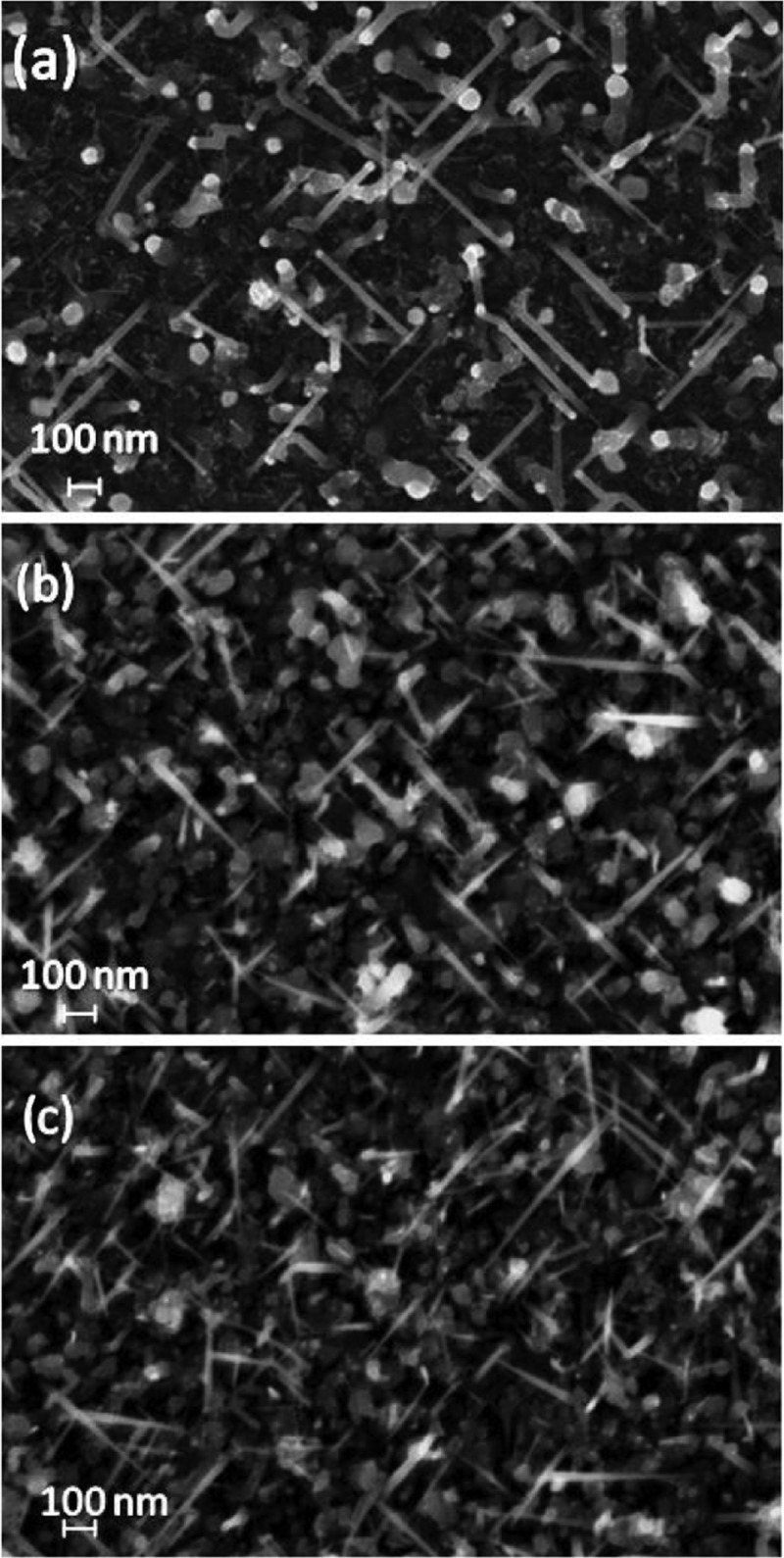
SEM images acquired in a planar view of the SiNW samples deposited at the plasma power of 20 W and setting the chamber pressure at (a) 20 mTorr, (b) 35 mTorr, and (c) 50 mTorr.
The qualitative observation of the SEM analysis, shown in Figure 1, preliminary suggests that at 50 mTorr the size of the NWs decreases with respect to the low-pressure conditions. This aspect is better quantified from the calculation of the SiNW size distribution, reported in Figure 2 as a function of their diameter for several chamber partial pressures of 20 mTorr (green symbols), 35 mTorr (red), and 50 mTorr (black). The graphs in the figure confirm that the NWs grown at 50 mTorr present a density distribution peaked at diameters smaller than those grown at 20 and 35 mTorr. At 5 nm, the SiNW distribution provides density values of about 3 × 10⁷ (20 mTorr), 4 × 10⁷ (35 mTorr), and 2 × 108 cm–2 nm–1 (50 mTorr), respectively.
Figure 2.
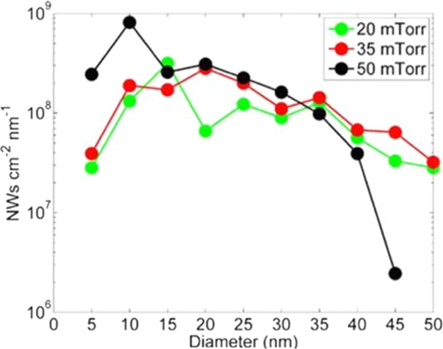
SiNWs size distribution determined by SEM images analysis for the samples deposited at 20 W of plasma power and 20 mTorr (green), 35 mTorr (red), and 50 mTorr (black) of chamber partial pressure.
Figure 3 reports the SEM images of the SiNWs grown at a constant pressure of 50 mTorr when the plasma power varies between 20 and 40 W. From the figure, we can see that the SiNWs grown at a power of 20 and 30 W are almost similar in density and size, while at 40 W, they drastically decrease in density and increase in dimension. Moreover, the presence of roughness on the substrate surface testifies the evident formation of Si by noncatalyzed growth.
Figure 3.
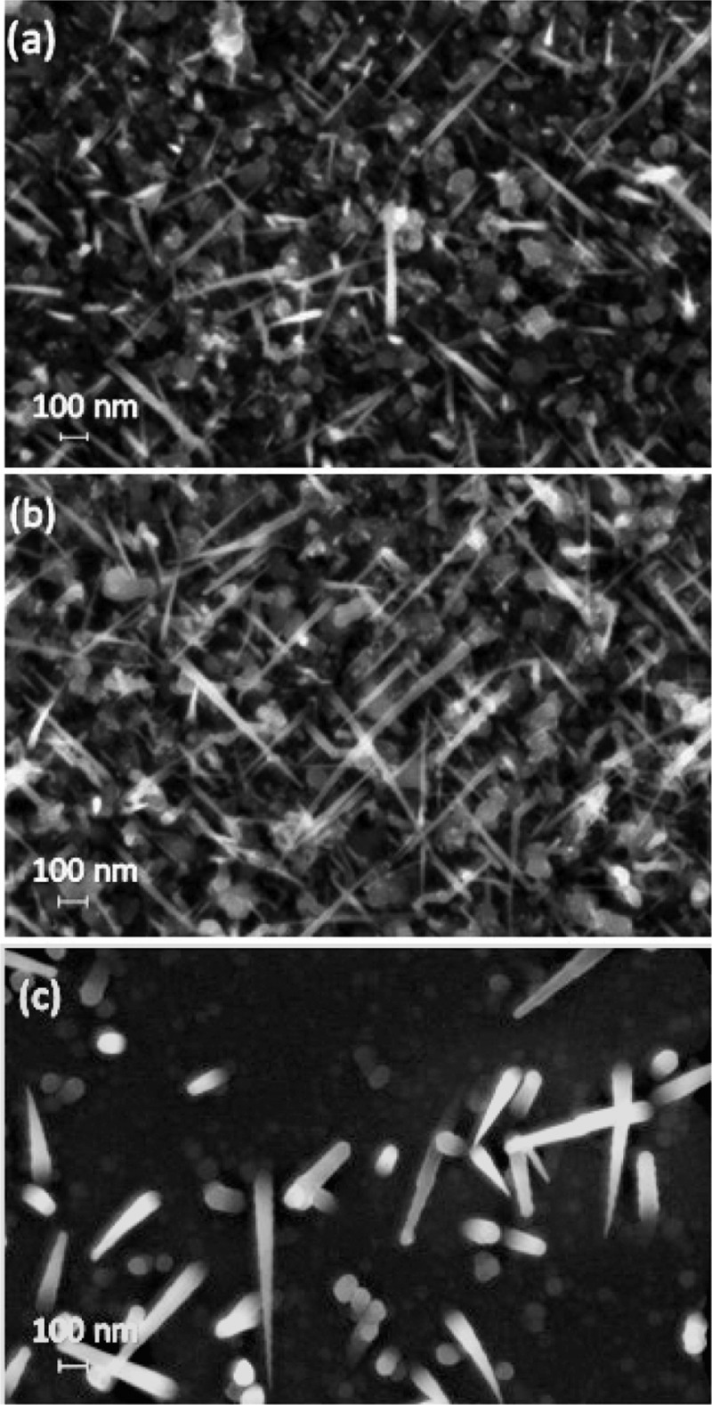
SEM images acquired in a planar view of the SiNW samples deposited at the Ar/SiH4 gas pressure of 50 mTorr by varying the plasma power: (a) 20 W, (b) 30 W, and (c) 40 W.
The density results can be quantitatively understood by comparing the size distribution for the different cases. Figure 4 displays the SiNWs size density distributions calculated by the SEM images analysis shown in Figure 3, i.e., for the samples deposited at 50 mTorr and 20 W (black), 30 W (red), and 40 W (green). The size distributions at 20 and 30 W are quite similar and peak at about 10 nm, showing that the plasma power in this range does not play a role in the SiNW diameters and confirming what is observed before, i.e., the pressure plays a major role in this process. At 40 W, however, the curve demonstrates a size distribution centered at ∼60 nm. The density of SiNWs obtained at plasma powers of 20, 30, and 40 W is, respectively, of the order 1 × 10¹⁰, 1.1 × 10¹⁰, and 4.8 × 108 cm–2. The low density of SiNWs grown at a power of 40 W is attributed to the noncatalyzed growth process, which under these conditions, becomes competitive compared to the catalyzed one. Large size is attributed to the fact that the small gold nanoparticles become buried during the competitive and fast SiH4 dissociation uncatalyzed process.18
Figure 4.
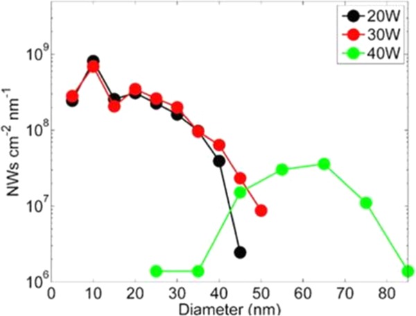
SiNWs size distribution calculated by SEM images analysis for the samples deposited at 50 mTorr and 20 W (black), 30 W (red), and 40 W (green).
To further investigate the presence of SiNWs with quantum size, the samples have been observed by TEM analysis since the SEM resolution is not sufficient to resolve objects below 5 nm. Figure 5 illustrates the TEM analysis obtained on the SiNWs at 20 W and 20 mTorr. The images in (a), (b), and (c) are taken in high-resolution mode and report SiNWs with diameters, respectively, of 2.8, 3.5, and 4 nm. The image in (d) represents an energy-filtered TEM acquired at 16 eV, i.e., close to the bulk Si plasmon excitation loss, with an energy window of 4 eV. The SiNW diameters measured correspond, respectively, to 2.8, 3.5, 4 and 3.5 nm. This demonstrates the presence of SiNWs with sizes smaller than 5 nm.
Figure 5.
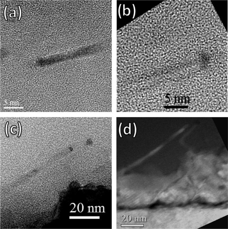
TEM acquired on the SiNWs grown at 20 W and 20 mTorr, imaged in high-resolution TEM mode (a–c) and in energy-filtered TEM mode by selecting the 16 eV plasmon peak (d). The SiNW diameters measured correspond, respectively, to 2.8, 3.5, 4, and 3.5 nm.
This result has to be attributed to the high partial pressure experienced by the metallic catalytic particle, liquid in the eutectic phase reached during the deposition, favoring the survival of the critical nucleus of Si precipitated after supersaturation. During the CVD deposition, the Si wafer with the Au dots on the surface is brought to 390 °C, a temperature higher than the Au–Si eutectic temperature. The Au nanodots in contact with the Si substrate form small liquid droplets of Au/Si eutectic alloy. The Gibbs–Thomson equation in this case is20
| 1 |
where Δμw = μw – μv, Δμb = μb – μv, and μw, μv, μb are the effective chemical potentials of Si in the NWs, in the vapor, and in the bulk state, respectively, Ω is the atomic volume of Si, and α and rd are the NW surface free energy and the droplet radius, respectively. For very small eutectic droplets, the inequality μw > μv is verified due to the large surface-to-volume ratio of the NWs. During surface diffusion, the droplet size can increase and reach a critical diameter, ruled by the allowed composition constrain in the droplet21 to allow the SiNW growth. Equation 1 hence sets a lower limit on the SiNWs that can grow under specific growth conditions. The experimental evidence for the minimum SiNW width has been also demonstrated by experimental data.20 The explanation provided is that if the chamber pressure is increased, μw increases leading to a more negative Δμb and allowing for the growth of small SiNWs.
Moreover, Tan demonstrated that while the minimum droplet radius rd is univocally determined (through the thermodynamic relation eq 1) by the vapor pressure conditions, there is not a thermodynamic constrain for the radius rNW cylindrical SiNW. As a consequence, the interplay between initial droplet geometry and the kinetic conditions implemented during the growth could also allow for the growth of smaller NWs, consistent with the fact that our size distributions tend to a finite value close to the 0 size for some process parameter settings (see Figure 4, red and black lines). The results presented demonstrate that SiNWs with sizes ranging between 2.5 and 80 nm can be synthesized. For applications where a uniform size is needed, other approaches can be envisaged, such as by controlling and fixing the catalyst size or by using lithographic mask constraints.27
Conclusions
In this work, a study on the formation of SiNWs with diameters as small as 5 nm, grown by VLS in the plasma-based CVD system, is reported. It is shown that the nanostructures can be obtained at pressures in the range between 20 and 50 mTorr. The peak of the size distribution appears at smaller sizes as the pressure increases. If the plasma power changes between 20 and 30 W, it plays a limited role in the size of SiNWs. The density value of SiNWs reached is as high as 1.1 × 1010 cm–2. To our knowledge, this is the first study where SiNWs as thin as 2.8 nm are obtained through direct deposition by VLS-CVD.
Acknowledgments
The authors wish to thank Salvatore Di Franco (CNR-IMM) for valuable help and expert support in several stages of the samples preparation. R.A.P. wishes to mention the National Program BEYOND NANO Upgrade (CUP G66J17000350007) for financial support.
The authors declare no competing financial interest.
References
- Cui Y.; Lieber C. M. Functional nanoscale electronic devices assembled using silicon nanowire building blocks. Science 2001, 291, 851–853. 10.1126/science.291.5505.851. [DOI] [PubMed] [Google Scholar]
- Zhang A.; Zheng G.; Lieber C.. Nanowires: Building Blocks for Nanoscience and Nanotechnology; Springer, 2016; ISBN 978-3-319-41979-4. [Google Scholar]
- Hasan M.; Huq M. F.; Mahmood Z. H. A review on electronic and optical properties of silicon nanowire and its different growth techniques. SpringerPlus 2013, 2, 151–160. 10.1186/2193-1801-2-151. [DOI] [PMC free article] [PubMed] [Google Scholar]
- Reed B. W.; Chen J. M.; MacDonald N. C.; Silcox J.; Bertsch G. F. Fabrication and STEM/EELS measurements of nanometer-scale silicon tips and filaments. Phys. Rev. B 1999, 60, 5641–5652. 10.1103/PhysRevB.60.5641. [DOI] [Google Scholar]
- Kikkawa J.; Takeda S.; Sato Y.; Terauchi M. Enhanced direct interband transitions in silicon nanowires studied by electron energy-loss spectroscopy. Phys. Rev. B 2007, 75, 245317 10.1103/PhysRevB.75.245317. [DOI] [Google Scholar]
- Voon L. C.; Zhang Y.; Lassen B.; Willatzen M.; Xiong Q.; Eklund P. C. Electronic Properties of Semiconductor Nanowires. J. Nanosci. Nanotechnol. 2008, 8, 1–26. 10.1166/jnn.2008.N03. [DOI] [PubMed] [Google Scholar]
- Yi K. S.; Trivedi K.; Floresca H. C.; Yuk H.; Hu W.; Kim M. J. Room-Temperature Quantum Confinement Effects in Transport Properties of Ultrathin Si Nanowire Field-Effect Transistors. Nano Lett. 2011, 11, 5465–5470. 10.1021/nl203238e. [DOI] [PubMed] [Google Scholar]
- Puglisi R. A.; Garozzo C.; Bongiorno C.; Di Franco S.; Italia M.; Mannino G.; Scalese S.; La Magna A. Molecular Doping applied to Si Nanowires array based Solar Cells. Sol. Energy Mater. Sol. Cells 2015, 132, 118–122. 10.1016/j.solmat.2014.08.040. [DOI] [Google Scholar]
- Peng K.; Lu A.; Zhang R.; Lee S. T. Motility of Metal Nanoparticles in Silicon and Induced Anisotropic Silicon Etching. Adv. Funct. Mater. 2008, 18, 3026–3035. 10.1002/adfm.200800371. [DOI] [Google Scholar]
- McSweeney W.; Lotty O.; Mogili N. V. V.; Glynn C.; Geaney H.; Tanner D.; Holmes J. D.; O’Dwyer C. Doping controlled roughness and defined mesoporosity in chemically etched silicon nanowires with tunable conductivity. J. Appl. Phys. 2013, 114, 034309 10.1063/1.4813867. [DOI] [Google Scholar]
- Lotty O.; Petkov N.; Georgiev Y. M.; Holmes J. D. Porous to Nonporous Transition in the Morphology of Metal Assisted Etched Silicon Nanowires. Jpn. J. Appl. Phys. 2012, 51, 11PE03 10.1143/JJAP.51.11PE03. [DOI] [Google Scholar]
- Wagner R. S.; Ellis W. C. Vapor-liquid-Solid Mechanism of Single Crystal Growth. Appl. Phys. Lett. 1964, 4, 89–90. 10.1063/1.1753975. [DOI] [Google Scholar]
- Akhtar S.; Usami K.; Tsuchiya Y.; Mizuta H.; Oda S. Vapor-Liquid-Solid Growth of Small- and Uniform-Diameter Silicon Nanowires at Low Temperature from Si2H6. Appl. Phys. Express 2008, 1, 014003 10.1143/APEX.1.014003. [DOI] [Google Scholar]
- Meng C. Y.; Shih B. L.; Lee S. C. Silicon nanowires synthesized by vapor–liquid–solid growth on excimer laser annealed thin gold film. J. Nanopart. Res. 2007, 9, 657–660. 10.1007/s11051-005-4631-1. [DOI] [Google Scholar]
- Das Kanungo P.; Zakharov N.; Bauer J.; Breitenstein O.; Werner P.; Goesele U. Controlled in situ boron doping of short silicon nanowires grown by molecular beam epitaxy. Appl. Phys. Lett. 2008, 92, 263107 10.1063/1.2953702. [DOI] [Google Scholar]
- Sivakov V.; Andra G.; Himcinschi C.; Gosele U.; Zahn D. R. T.; Christiansen S. Growth peculiarities during vapor–liquid–solid growth of silicon nanowhiskers by electron-beam evaporation. Appl. Phys. A 2006, 85, 311–315. 10.1007/s00339-006-3675-0. [DOI] [Google Scholar]
- Fontcuberta i Morral A.; Arbiol J.; Prades J. D. Synthesis of silicon nanowires with wurtzite crystalline structure by using standard chemical vapor deposition. Adv. Mater. 2007, 19, 1347–1351. 10.1002/adma.200602318. [DOI] [Google Scholar]
- Garozzo C.; La Magna A.; Mannino G.; Privitera V.; Scalese S.; Sberna P. M.; Simone F.; Puglisi R. A. Competition between uncatalyzed and catalyzed growth during the plasma synthesis of Si nanowires and its role on their optical properties. J. Appl. Phys. 2013, 113, 214313 10.1063/1.4809557. [DOI] [Google Scholar]
- Puglisi R. A.; Mannino G.; Scalese S.; La Magna A. Silicon Nanowires Obtained by Low Temperature Plasma-Based Chemical Vapor Deposition. MRS Online Proc. Libr. 2012, 1, 139–144. 10.1557/opl.2012.718. [DOI] [Google Scholar]
- Westwater J.; Gosain D. P.; Tomiya S.; Usui S.; Ruda H. Growth of silicon nanowires via gold/silane vapor–liquid–solid reaction. J. Vac. Sci. Technol., B 1997, 15, 554–557. 10.1116/1.589291. [DOI] [Google Scholar]
- Tan T. Y.; Li N.; Gösele U. Is there a thermodynamic size limit of nanowires grown by the vapor-liquid-solid process?. Appl. Phys. Lett. 2003, 83, 1199–1201. 10.1063/1.1599984. [DOI] [Google Scholar]
- Kodambaka S.; Tersoff J.; Reuter M. C.; Ross F. M. Diameter-Independent Kinetics in the Vapor-Liquid-Solid Growth of Si Nanowires. Phys. Rev. Lett. 2006, 96, 096105 10.1103/PhysRevLett.96.096105. [DOI] [PubMed] [Google Scholar]
- Dhalluin F.; Desré P. J.; Den Hertog M. I.; Rouvière J.-L.; Ferret P.; Gentile P.; Baron T. Critical condition for growth of silicon nanowires. J. Appl. Phys. 2007, 102, 094906 10.1063/1.2811935. [DOI] [Google Scholar]
- Shir D.; Liu B. Z.; et al. Oxidation of silicon nanowires. J. Vac. Sci. Technol., B 2006, 24, 1333–1336. 10.1116/1.2198847. [DOI] [Google Scholar]
- Puglisi R. A.; Lombardo S.; Nicotra G.; Spinella C.; Ammendola G.; Gerardi C. Partial self-ordering observed in silicon nanoclusters deposited on silicon oxide substrate by chemical vapor deposition. Phys. Rev. B 2005, 71, 125322 10.1103/PhysRevB.71.125322. [DOI] [Google Scholar]
- Tan T. Y.; Li N.; Gosele U. On the thermodynamic size limit of nanowires grown by the vapor-liquid-solid process. Appl. Phys. A: Mater. Sci. Process. 2004, 78, 519–526. 10.1007/s00339-003-2380-5. [DOI] [Google Scholar]
- Garozzo C.; Puglisi R. A.; Bongiorno C.; Scalese S.; Rimini E.; Lombardo S. Selective diffusion of gold nanoparticles on nano-templated substrates realised by diblock copolymers self-assembling. J. Mater. Res. 2011, 26, 240–246. 10.1557/jmr.2010.19. [DOI] [Google Scholar]


