Abstract
Staggered gap radial heterojunctions based on ZnO-CuxO core-shell nanowires are used as water stable photocatalysts to harvest solar energy for pollutants removal. ZnO nanowires with a wurtzite crystalline structure and a band gap of approximately 3.3 eV are obtained by thermal oxidation in air. These are covered with an amorphous CuxO layer having a band gap of 1.74 eV and subsequently form core-shell heterojunctions. The electrical characterization of the ZnO pristine and ZnO-CuxO core-shell nanowires emphasizes the charge transfer phenomena at the junction and at the interface between the nanowires and water based solutions. The methylene blue degradation mechanism is discussed taking into consideration the dissolution of ZnO in water based solutions for ZnO nanowires and ZnO-CuxO core-shell nanowires with different shell thicknesses. An optimum thickness of the CuxO layer is used to obtain water stable photocatalysts, where the ZnO-CuxO radial heterojunction enhances the separation and transport of the photogenerated charge carriers when irradiating with UV-light, leading to swift pollutant degradation.
Subject terms: Photocatalysis, Nanowires
Introduction
To answer the requirement of decreasing the use of fossil fuels researchers are directing their efforts towards harvesting solar, wind, bio-mass and other forms of renewable energy1,2. Developing suitable and sustainable materials for applications such as solar cells, batteries, H2 generation and pollutants removal via photocatalysis represents a sensible approach for achieving this goal1,3–6. In recent years, the trend in obtaining new material architectures with improved functionalities shifted towards nanoscale engineering, the advantages include minimized substance consumption and improvement of device performances7. Among nanostructures, nanowires are particularly remarkable, because of their high aspect ratio and large surface area8 they can show enhanced optical properties such as light trapping, antireflection, and high absorption9–11. To be technologically feasible, nanowire fabrication must be fast, controlled and easily scalable which is achievable with appropriate synthesis routes and material combinations12–14. For semiconductors with low exciton and carrier diffusion lengths, free charge carriers can be generated and transferred with a higher efficiency for radial heterojunctions than for planar/normal ones15,16 due to the orthogonal directions of the light absorption and charge in core-shell radial heterojunctions. In this particular case, photon absorption takes place along the nanowire length, while the separation of charges takes place within the diameter. Arrays of core-shell nanowires and/or nanowire nanoparticle junctions based on Pd/ZnO, ZnO/ZnFe2O4, ZnO/Zn2TiO4, ZnO/ZnS/Au, TiO2/CuO, Si/Cu2O are reported to be used in photocatalytic applications such as water splitting and pollutants removal3,17–22, dissolution processes not being investigated.
As a cost-effective alternative for obtaining photocatalysts that are efficient and also water stable, in this work ZnO–CuxO core-shell nanowire arrays are used as p-n staggered gap radial heterojunctions. A good photocatalytic efficiency and protecting the ZnO nanowire from dissolution are advantages of this system. Zinc oxide is an n-type semiconductor with a direct wide band-gap (Eg = 3.3 eV), a large exciton binding energy (~60 meV) and high electron mobility13,23,24. For aqueous environment applications, a major disadvantage to be overcome is the ZnO dissolution. This process was observed previously for nanoparticles25–29, thin films30,31, porous nanosheets32, and even nanowires33–35, being enhanced under UV-light irradiation32,36, but was not discussed, up to now, to our knowledge, in relation with its photocatalytic response. On the other hand, copper oxide is a p-type semiconductor, abundant, cheap and can be found in the form of: Cu2O, with a direct band-gap of 2.0 eV, CuO, with an indirect band-gap of 1.2–1.6 eV37,38 or a mixture between them, particular composition being a consequence of the preparation method.
In our study, ZnO nanowires were obtained by thermal oxidation in air and covered with CuxO layers deposited by magnetron sputtering leading to water stable photocatalysts. Electrical charges transfer along the radial junction and between the ZnO-CuxO core-shell nanowires and an aqueous media are investigated for different thickness of the shell layer in order to explain the mechanism of the photocatalytic degradation of methylene blue. Herein, for ZnO nanowires, two concurrent processes are considered: its dissolution which leads to zinc ions release in the solution and the charge carriers photogeneration. The dissolution process of ZnO nanowires with the covering by CuxO decreases with increasing the CuxO thickness, while the charges photogeneration improves. When reaching an optimum thickness of CuxO, the staggered gap radial heterojunction based on ZnO-CuxO nanowires has a better photocatalytic response than the pristine ZnO nanowires, being in the same time water stable.
Materials and Methods
Materials
All solvents and chemical reagents are commercially available being purchased and used without further purification.
Preparation of core-shell nanowires arrays
The synthesis of the ZnO-CuxO core-shell nanowires was described in our previous paper39. Thus, ZnO nanowires were prepared using 2 cm2 zinc foils (Alfa Aesar, 99.99%). Initially, the metallic foils were cleaned for 5 min in an ultrasonic bath (acetone and isopropyl alcohol), followed by repeated rinsing in deionized water and dried under nitrogen gas flow. The cleaned zinc substrates were thermally oxidized in air in a convection oven at 500 °C for 12 h. The length and diameters of the ZnO nanowires are controlled by the thermal oxidation parameters (temperature and time), as reported in our previous study23,24. Further, the ZnO-CuxO core-shell nanowires were obtained by depositing copper oxide thin layers in a TECTRA magnetron sputtering system from a CuO target (Kurt Lesker)39. The pressure used was 5.4 × 10⁻³ mbar in Ar atmosphere and the applied power was 100 W. By changing the deposition time from 6 min to 18 min and 30 min copper oxide thin films with different thicknesses were obtained, samples denoted with ZnO-CuxO_1, ZnO-CuxO_2 and ZnO-CuxO_3, respectively39. Also, for comparison reasons, a copper oxide layer was deposited on Si/SiO2 substrate for 30 min (sample denoted with CuxO).
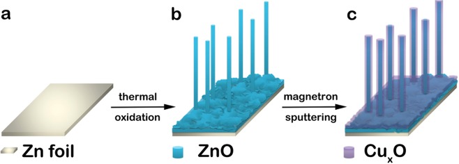
The stages implicated in the synthesis of the ZnO-CuxO core-shell nanowires39 are illustrated in Fig. 1.
Figure 1.
Illustration of the preparation procedures for ZnO – CuxO core-shell nanowire arrays: (a) cleaning the Zn foil used for substrate and growth site, (b) synthesizing ZnO nanowires by thermal oxidation in air and (c) obtaining ZnO – CuxO core-shell nanowire arrays by depositing a layer of CuxO by magnetron sputtering.
Characterization
The characterization techniques used for evaluating the properties of the ZnO-CuxO core-shell nanowires were detailed in our previous paper39. Thus, the structural, morphological and optical properties of the thermally oxidized Zn foil and of the samples covered with copper oxide were evaluated using a Bruker AXS D8 Advance instrument with Cu Kα radiation (λ = 0.154 nm), a Zeiss Merlin field emission scanning electron microscope (FESEM), a Perkin–Elmer Lambda 45 UV–vis spectrophotometer equipped with an integrating sphere and a FL 920 Edinburgh Instruments spectrometer with a 450 W Xe lamp excitation and double monochromators, respectively39. In the X-ray diffraction (XRD) measurements, the source was operated at 40 kV and 40 mA eliminating Kβ radiation with a nickel filter. Also, transmission electron microscopy (TEM) investigations using several techniques were performed on a Cs probe corrected JEM ARM 200F microscope provided with a JEOL energy-dispersive X-ray spectroscopy (EDS). Scanning transmission electron microscopy (STEM) was combined with the EDS analytical technique in order to map the local chemical composition. For TEM analysis, the ZnO and ZnO-CuxO nanowires were dispersed into isopropyl alcohol by sonication and in order to be investigated a drop of solution containing nanowires was placed on the TEM grid. The chemical analysis was obtained by means of EDX39.
X-Ray Photoelectron Spectroscopy (XPS) has been performed in an AXIS Ultra DLD (Kratos Surface Analysis) setup equipped with an 180° hemispherical analyzer39, using Al Kα1 (1486.74 eV) radiation produced by a monochromatized X-Ray source at operating power of 300 W (12 kV × 25 mA). The base pressure in the analysis chamber was at least 1.0 × 10⁻⁸ mbar. Partially charge compensation was reached by using a flood gun operating at 1.52 A filament current, 2.73 V charge balance, 2.02 V filament bias. The survey spectra have been recording using hybrid lens mode, 80 eV pass energy, slot aperture. High resolution core level spectra have been recorded using Field of View 2 lens mode, 20 eV pass energy, 110 µm aperture. The binding energy scale was calibrated to the C 1 s standard value of 284.6 eV.
The electrochemical studies were carried out using a VoltaLab PGZ100 potentiostat, running VoltaMaster 4.0 software. The experiments were done in a three-electrodes configuration, which consisted of a saturated calomel electrode (SCE) as reference, a platinum wire as auxiliary and the ZnO nanowires or ZnO-CuxO core-shell nanowires as working electrode. The electrochemical impedance spectroscopy (EIS) measurements were made in 0.1 M KCl, at open circuit potential (OCP) values, using a perturbation of 10 mV for 60 harmonic frequencies ranging from 100 kHz to 0.1 Hz at 10 steps/decade. The impedance spectra were analysed by fitting with an equivalent electrical circuit using ZView software (Scribner Associates, USA)40 containing as parameters Rs, CPE and Ws. The Rs consists of the solution and the bulk composite resistances. The constant phase elements, defined as:
| a |
is modelled as a non-ideal capacitor where the capacitance C describes the charge separation at the double layer interface and the α exponent is due to the heterogeneity of the surface.
The definition of the Warburg element used is:
| b |
where Rdiff is a diffusion resistance of electroactive species, τ is a time constant depending on the diffusion rate (τ = l2/D, where l is the effective diffusion thickness, and D is the effective diffusion coefficient of the species), and n = 0.50 for a perfect uniform flat interface41.
The photocatalytic activity of the synthesized samples under UV irradiation was evaluated by measuring the optical absorbance of the methylene blue (MB) solution at 665 nm wavelength using an UV–visible spectrophotometer (Evolution 220, Thermo Scientific). In this respect, a 15 watts UV bench lamp that emitted at wavelength 312 nm was used as a light source. The tests were carried out in a flask type reactor of glass with 10 mL of methylene blue aqueous solution adjusted to be 35 μM and pH of 7 where the zinc foils containing arrays of nanowires were immersed. The dye degradation was performed under constant stirring, in dark and UV conditions. After every 20 min of UV irradiation, the solution was withdrawn in order to collect its optical absorbance spectrum. During the UV irradiation, the MB solution was kept at 24 °C by means of circulating bath model TC120 with refrigerator from Grant. To make a comparison of the photocatalytic activity of the investigated samples, the degradation efficiency was estimated using the equation:
| c |
where, C0 is the initial value of the dye concentration, C is the value of dye concentration at t, time. Also, the degradation rate constant was obtained from the slope of the linear fitting of ln(C0/C) vs. time, taking into consideration that the photocatalytic degradation of MB is classified as the first-order Langmuir–Hinshelwood kinetics described by the equation:
| d |
where C0 is the initial concentration of MB, C is the concentration of MB at a time t, and k is the first-order degradation rate constant.
Results and Discussion
Morphological, structural, compositional and optical properties
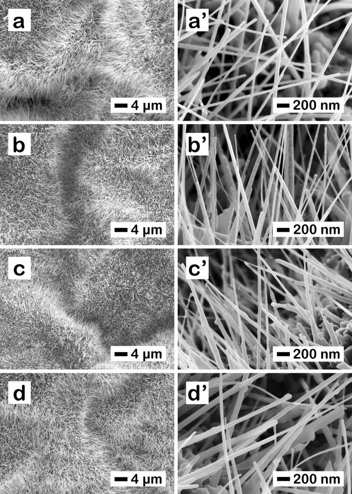
The morphology investigation revealed that the ZnO nanowires have a high density onto the Zn foil, Fig. 2, with lengths up to 30 µm and diameters of about 30 nm, Fig. 2(a,a’). The deposition of the CuxO layer led to an increase in the diameter of the ZnO-CuxO nanostructure. Consequently, at 6 min (Fig. 2(b,b’)), 18 min (Fig. 2(c,c’)) and 30 min (Fig. 2(d,d’)) deposition time, the thickness of the nanowire increased, in average with about 10 nm for ZnO-CuxO_1, 20 nm for ZnO-CuxO_2 and 30 nm for ZnO-CuxO_3, respectively. Thus, the increase in the diameter of the ZnO nanowires after their coating with the CuxO layer suggests the formation of a heterojunction between the two semiconductors.
Figure 2.
FESEM images at different magnifications for the as prepared (a,a’) ZnO nanowires, (b,b’) ZnO – CuxO_1, (c,c’) ZnO – CuxO_2 and (d,d’) ZnO – CuxO_3 core-shell nanowires.
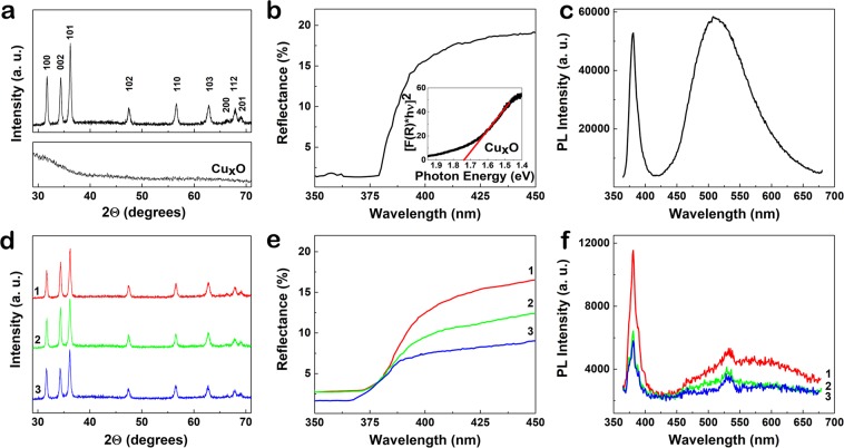
The XRD analysis showed the hexagonal wurtzite crystalline structure of the ZnO nanowires, Fig. 3(a) up, where the Miller indexes are depicted for every peak: (100), (002), (101), (102), (110), (103), (200), (112) and (201) corresponding to JCPDS file no. 36–1451. The same reflecting planes were also identified in the XRD patterns of ZnO-CuxO_1, ZnO-CuxO_2 and ZnO-CuxO_3 core- shell nanowire samples, Fig. 3(d). It has to be noticed that in the diffractograms of the core-shell nanowire arrays there is no additional peak that can be related with the CuxO layer. The result can be explained taking into account the amorphous nature of the copper oxide films deposited by radio-frequency magnetron sputtering42,43 evidenced by the XRD pattern of the CuxO film deposited on Si/SiO2 substrate (Fig. 3(a) down) in the same condition with that obtained in the case of ZnO-CuxO_3 sample.
Figure 3.
(a,d) XRD, (b,e) reflectance and (c,f) photoluminescence spectra of (a – up, b,c) ZnO and (d–f) ZnO-CuxO core shell nanowires: ZnO-CuxO_1 (red curves), ZnO-CuxO_2 (green curves) and ZnO-CuxO_3 (blue curves) nanowires; (a–down) XRD and (b – inset) Kubelka-Munk representation of the CuxO layer with the longest deposition time.
The reflectance measurements revealed that the energy band gap of ZnO does not alter significantly with the deposition of the CuxO shell layers being around 3.3 eV (Fig. 3(b,e)). The energy band gap of the CuxO on SiO2/Si was estimated from the Kubelka-Munk representation to be 1.74 eV (inset of Fig. 3(b)), a value between the ones of CuO and Cu2O nanostructures37,38. A decrease in reflectance in the visible range with the increase in thickness of CuxO layer is noticed, going from 19% for ZnO nanowires down to 17% for ZnO-CuxO_1, 12.5% for ZnO-CuxO_2 and 7.5% for ZnO-CuxO_3 core-shell nanowires. Thus, the ZnO nanowires covered with the thickest CuxO layer (15 nm) give rise to an increase of about 40% in the absorbance of the resulting ZnO-CuxO core-shell nanowires in the visible part of the solar spectrum, useful for photocatalysis applications.
For ZnO nanowires, the photoluminescence spectrum (Fig. 3(c)) exhibits a typical response for this semiconductor when being excited with 350 nm. The sharp peak at 380 nm, corresponds to the band-to-band transitions in ZnO (excitonic peak), while the broad intense emission band in the visible region, attributed to optical active defects in ZnO24,25. A decrease in the intensities of the two emission bands takes place when the ZnO nanowires are covered with CuxO layers. Also, a change in the ratio of the emission bands is observed, Fig. 3(f). This effect is in agreement with the compensation of ZnO surface defects by the covering with CuxO layers, being probably due to decrease of scattering processes44.
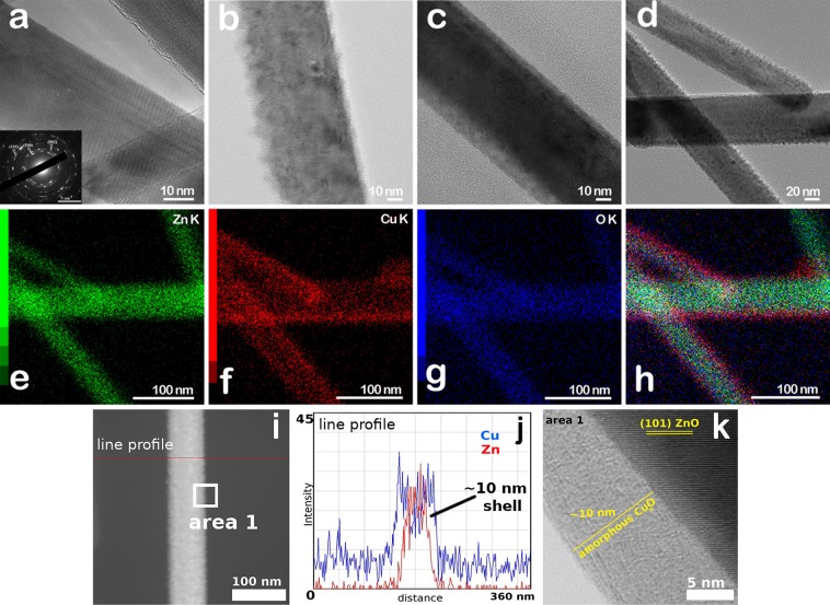
In Fig. 4(a–d), the TEM images show ZnO nanowires and ZnO-CuxO core-shell nanowires proving the difference in the shell thicknesses with increasing the deposition time, in accordance with the FESEM observations. Thus, the ZnO nanowires have diameters of about 30 nm while the shell thicknesses for the core-shell nanowires presents average values of about 5 nm for ZnO-CuxO_1, 10 nm for ZnO-CuxO_2 and 15 nm for ZnO-CuxO_3. For ZnO nanowires, the SAED pattern evidenced the wurtzite phase (inset of Fig. 4(a)) with the (101), (100) and (002) planes, consistent with the XRD analysis, while the CuxO layers were amorphous (Fig. 4(b–d)). Furthermore, the TEM image in Fig. 4(b) reveals that the surface of the ZnO-CuxO_1 core-shell nanowire is relative rough, probably due to discontinuities in the CuxO thin film, which does not entirely cover the ZnO nanowire surface. With increasing the CuxO thin film thickness, the surface of the core-shell nanowires becomes smoother, decreasing the number of possible pinholes in the CuxO layer and consequently leading to a complete coverage of the ZnO core for the samples denoted by ZnO-CuxO_3 (Fig. 4(d)). The elemental maps displayed in Fig. 4(e–h) demonstrate the spatial distribution of all constituting elements for the sample with the highest CuxO thickness, ZnO-CuxO_3. The Zn K-edge signals are emitted from the core area, while the Cu K-edge is seen at the edges, having O K-edge uniformly distributed along the nanowire, proving the heterojunction between ZnO and CuxO in the core-shell nanowire. The EDS line profile analysis by STEM mode and the HRTEM image (Fig. 4(i–k)) reveal also the formation of a core-shell structure in the nanowires consisting in a hexagonal wurtzite ZnO core and an amorphous CuxO shell. Additionally, TEM analysis confirm the diameters of the core-shell nanostructures determined by FESEM. Thus, the ZnO nanowires have diameters of about 30 nm while the shell thicknesses for the core-shell nanowires presents average values of about 5 nm for ZnO-CuxO_1, 10 nm for ZnO-CuxO_2 and 15 nm for ZnO-CuxO_3.
Figure 4.
TEM images of (a) ZnO nanowires having in the inset a SAED pattern proving the ZnO wurtzite phase and of (b-d) ZnO-CuxO core-shell nanowires with different shell thicknesses (with (b) ZnO-CuxO_1, (c) ZnO-CuxO_2 and (d) ZnO-CuxO_3), (e–h) Elemental maps of the same ZnO-CuxO_3 nanowires region, indicating spatially-resolved elemental distribution of Zn (green), Cu (red) O (blue), and their superposition, (i) STEM image, (j) EDS line profile analysis by STEM mode and (k) HRTEM image of area 1 of a ZnO-CuxO core-shell nanowire.
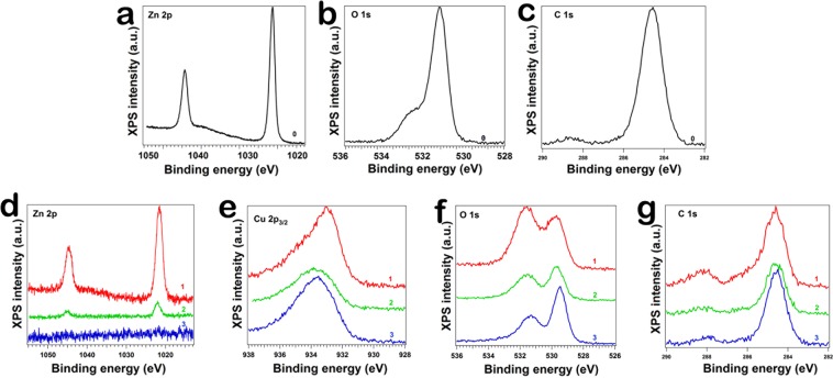
The XPS investigation was carried out to evidence the nature of bondings and to discover the Cu oxidation state in the CuxO layers. The core level spectra (Fig. 5) have been deconvoluted using Voigt profiles, based on the methods described in reference45 and are presented in Fig. S1 for Zn 2p levels, Fig. S2 for O 1 s levels and Fig. S3 for Cu 2p3/2 levels. The atomic composition, Table S1, has been determined by using the integral areas provided by the deconvolution procedure normalized at the atomic sensitivity factors46, taking into consideration a slight contamination of the surfaces with CO3.
Figure 5.
XPS spectra of the (a,d) Zn 2p levels, (b,f) O 1 s levels, (c,g) C 1 s levels and (e) Cu 2p3/2 levels, for pristine ZnO nanowires (a–c) and for ZnO-CuxO core-shell nanowires (d–g): ZnO-CuxO_1, ZnO-CuxO_2 and ZnO-CuxO_3 respectively.
The formation of ZnO is confirmed by XPS for the samples containing ZnO, ZnO-CuxO_1, ZnO-CuxO_2, with the signal fading when increasing the thickness of the CuxO layer. The XPS analysis has shown that the CuxO shell comprises a mixture between Cu2O and CuO having a ratio of about 3:1 for ZnO-CuxO_1 and a ratio of 1:1 for ZnO-CuxO_2 and ZnO-CuxO_3. Thus, the XPS results attested also the formation of a heterojunction between ZnO and CuxO in the core-shell nanowire.
Electrochemical properties
EIS was employed to investigate the electrical properties of the ZnO nanowires and ZnO-CuxO core-shell nanowires and to analyse the electron charge transfer between these nanowire arrays and water based solutions. EIS was carried out in 0.1 M KCl at OCP values, Fig. 6. The OCP values (−1.015 V for ZnO, −1.020 V for ZnO-CuxO_1, −1.025 V for ZnO-CuxO_2 and −1.020 V for ZnO-CuxO_3) were also recorded in 0.1 M KCl until a drift below 0.1 mV min−1 was reached. The obtained EIS included three main regions. The first region between 100 kHz and 100 Hz corresponding to the electron transfer and diffusion process. The second region between 100 Hz and 0.25 Hz, a semi-circular part due to pure electron transfer. The third region related to the frequency range below 0.25 Hz represented by an inverse loop is due to an inductive component. Thus, all characterized samples are eligible for charge transfer processes47.
Figure 6.
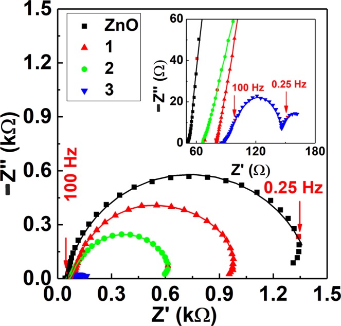
Nyquist representation of the EIS of ZnO nanowires (black squares) and of ZnO-CuxO core-shell nanowires: ZnO-CuxO_1 (red upward triangles), ZnO-CuxO_2 (green circles) and ZnO-CuxO_3 (blue downward triangles) recorded in 0.1 M KCl at OCP. The symbols represent the experimental data and the continuous lines the fitting results with the circuit in Fig. 7.
In agreement, the spectra were fitted with an equivalent electrical circuit, Fig. 7, formed by Rs attributed to electrochemical cell resistance, a constant phase element CPE1 in parallel with a resistor R1 and a Warburg impedance Ws corresponding to the electrolyte/electrode interface, followed by a parallel combination of a constant phase element CPE2 and a resistor R2 associated with ZnO-CuxO heterojunction.
Figure 7.
Equivalent electrical circuit used for fitting the EIS experimental data.
The EIS experiments revealed that, increasing the thickness of CuxO layer both real and imaginary impedance decreased. Data from analysis of EIS, Table 1, showed the cell resistance RΩ with values between 50 and 90 Ω increasing with CuxO thickness. On the other hand, the charge transfer resistances R1 and R2 decreased upon increasing the thickness of the CuxO, which can be associated with the protection of ZnO from dissolution, in agreement with CV studies.
Table 1.
Values of electrical equivalent circuit elements after fitting the experimental data in Fig. 6 with the equivalent circuit in Fig. 7.
| Sample | Rs (Ω) | R1 (Ω) | CPE1 | R2 (Ω) | CPE2 | Ws | ||||
|---|---|---|---|---|---|---|---|---|---|---|
| C1 (µF) | α1 | C2 (µF) | α2 | Rdiff (Ω) | Τ (ms) | N | ||||
| ZnO | 50.8 | 964.6 | 173.9 | 0.87 | 459.6 | 90.3 | 0.99 | 4.7 | 0.6 | 0.32 |
| ZnO-CuxO_1 | 77.9 | 581.6 | 152.7 | 0.88 | 345.9 | 114.2 | 0.99 | 19.6 | 6.7 | 0.33 |
| ZnO-CuxO_2 | 65.1 | 319.0 | 231.4 | 0.88 | 227.1 | 378.6 | 0.99 | 27.9 | 11.9 | 0.35 |
| ZnO-CuxO_3 | 87.3 | 32.4 | 463.5 | 0.99 | 30.9 | 413.9 | 1.0 | 29.1 | 14.8 | 0.37 |
Also, the interfacial capacitance C1 as well as the C2 of the ZnO-CuxO heterojunction showed higher values for thicker CuxO layer due to an increase of the electroactive surface area, whereas the heterogeneity parameter α1 reaches higher values concurring with smother surfaces for thicker CuxO. The roughness parameter α2 is approximatively 1 and remains constant, meaning that the ZnO-CuxO junction behaves as a pure capacitor. Nevertheless, the diffusion resistance as well as the diffusion process time constant increased with CuxO thickness, showing that when it reaches the maximum value, the faster interfacial charge transfer is attained for ZnO-CuxO_3.
Photocatalytic properties and dissolution effects
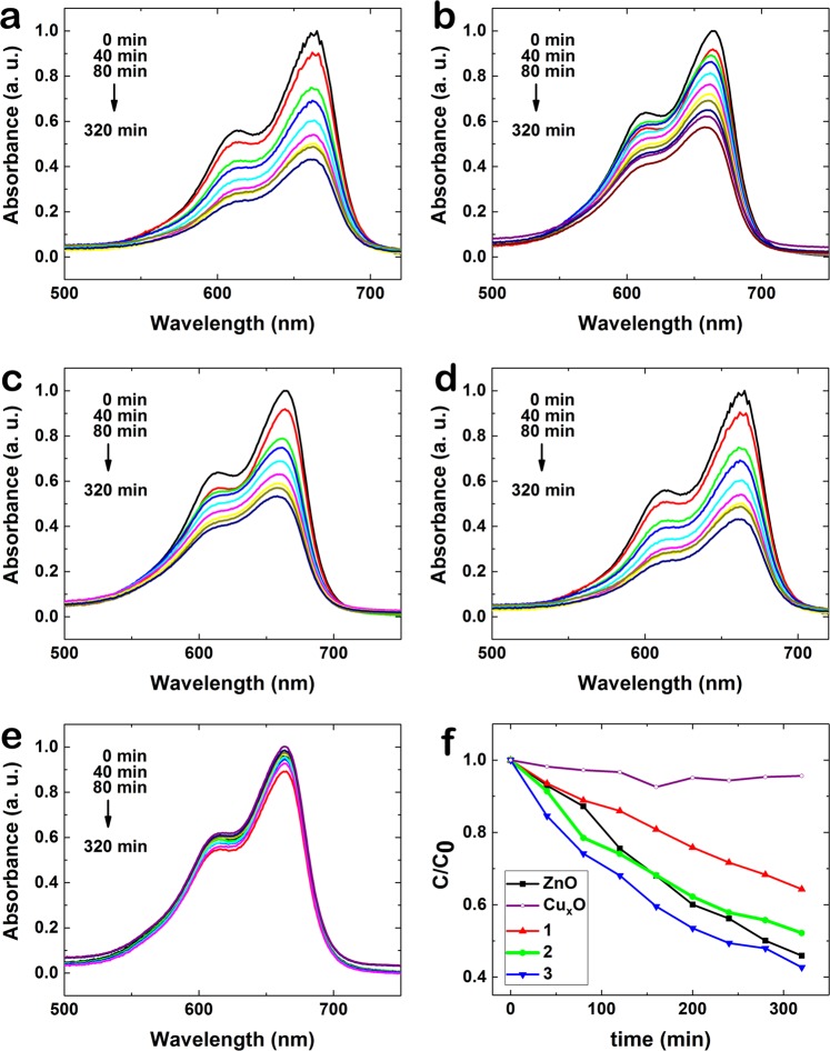
In order to demonstrate the photocatalytic efficiency of ZnO-CuxO nanostructures, the photodegradation of the model dye methylene blue (MB) was investigated and can be observed in Fig. 8, where the peaks of absorbance curves corresponding to MB decrease in time in the presence of ZnO (Fig. 8(a)), ZnO-CuxO_1 (Fig. 8(b)), ZnO-CuxO_2 (Fig. 8(c)), ZnO-CuxO_3 (Fig. 8(d)) and CuxO (Fig. 8(e)). The degradation profiles of MB in aqueous based solution under UV irradiation over time (Fig. 8(f)) show less steep curves of ZnO-CuxO_1 and ZnO-CuxO_2 than pristine ZnO nanowires.
Figure 8.
Absorption spectra showing time evolution of the degradation of MB in aqueous based solution under UV irradiation in the presence of (a) ZnO, (b) ZnO-CuxO_1, (c) ZnO-CuxO_2, (d) ZnO-CuxO_3 nanowires (e) CuxO film and (f) degradation profiles of MB in aqueous based solution under UV irradiation over time for all samples.
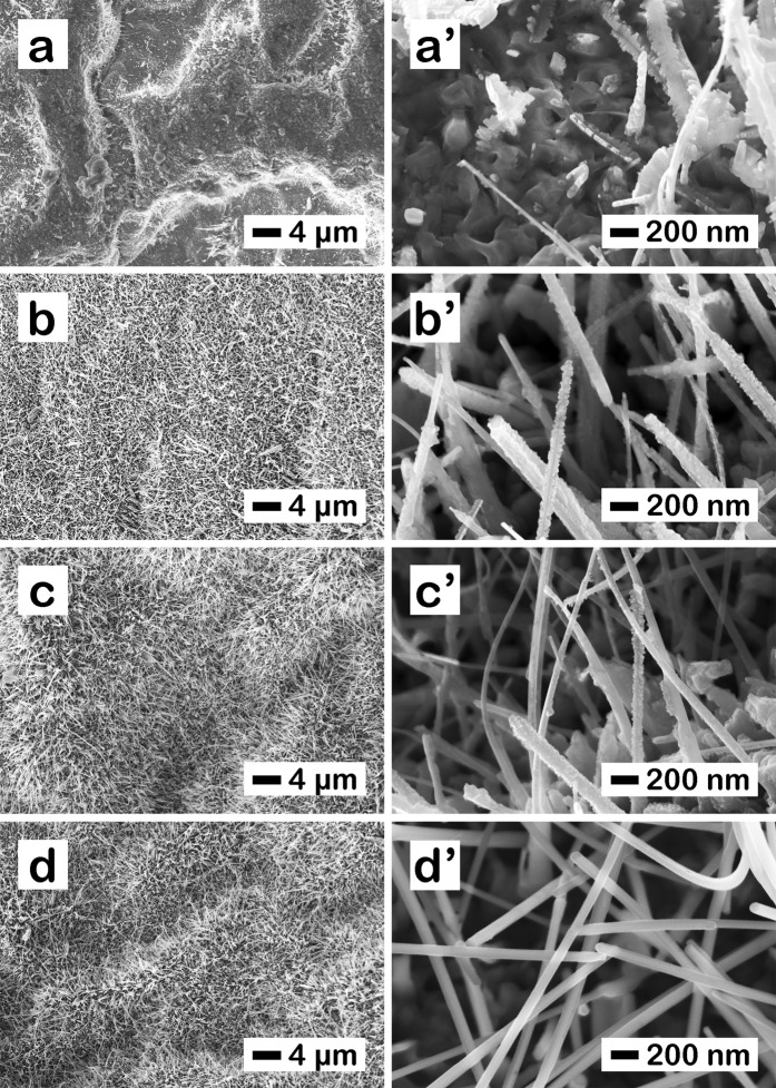
For a better understanding of the photocatalytic activity of our samples, FESEM images at different magnifications were made after the photocatalysis experiments (after immersion in water based solution and UV irradiation for at least 5 h, Fig. 9). The FESEM images revealed increased stability of the nanowires in aqueous based solutions with increasing shell thickness in agreement with the EIS results. ZnO pristine nanowires dissolve completely in 5 h (Fig. 9(a,a’)), ZnO-CuxO_1 and ZnO-CuxO_2 partially dissolve (Fig. 9(b,b’,c,c’), respectively) in 5 h, while ZnO-CuxO_3 nanowires remain morphologically unchanged (Fig. 9(d,d’)) after the photocatalysis experiments.
Figure 9.
FESEM images at different magnifications for (a,a’) ZnO, (b,b’) ZnO-CuxO_1, (c,c’) ZnO-CuxO_2 and (d,d’) ZnO-CuxO_3 nanowires after the photocatalysis experiments.
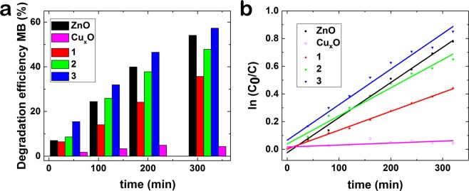
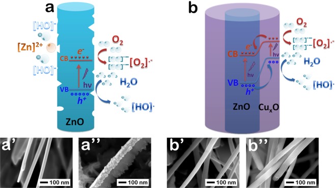
The degradation efficiency over time and the kinetics of the degradation of MB (ln(C0/C) vs. time) in the presence of ZnO, CuxO, ZnO-CuxO_1, ZnO-CuxO_2 and ZnO-CuxO_3 samples are shown in Fig. 10(a,b). An illustration of the mechanisms involved in the photodegradation of MB using ZnO and ZnO-CuxO nanowires is depicted in Fig. 11.
Figure 10.
(a) Photocatalysis degradation efficiency of MB over time and (b) kinetic curves for photocatalytic degradation of MB, under UV irradiation and in the presence of ZnO, ZnO-CuxO_1, ZnO-CuxO_2, ZnO-CuxO_3 nanowire arrays and CuxO film.
Figure 11.
The MB photocatalysis degradation mechanism under UV irradiation in the presence of (a) ZnO and (b) ZnO-CuxO_3 nanowires and the FESEM images of the samples (a’,b’) before and (a”,b”) after the photocatalysis experiment in each case, showing the (a’,a”) ZnO instability and (b’,b”) ZnO-CuxO_3 stability in aqueous based solutions.
The degradation of MB by ZnO occurs with 54% efficiency and 0.1518 h−1 degradation rate constant and follows distinct concurrent processes (dissolution of ZnO and photogeneration of charges) occurring either in the absence or under UV-light irradiation, in aqueous based solutions. The FESEM images taken before (Fig. 11(a’)) and after (Fig. 11(a”)) the photocatalysis experiments confirm the dissolution of ZnO nanowires in water based solution. The lower photocatalytic activity of the CuxO thin film (lower efficiency, 4%, and degradation rate constant, k = 0.0085 h−1) compared with the ZnO nanowires can be given by the thickness of the layer and its 2D morphology which lead to the absorption of a low number of photons giving rise to a small number of photogenerated charges and thus e− and h+ on its surface. For planar structures, the photogenerated carrier number increases with the thicknesses of the films48–51.
The ZnO-CuxO_1 and ZnO-CuxO_2 nanowires degrade MB with a higher efficiency (35% and 47% respectively) and a higher degradation rate constant (k = 0.0816 h−1 and k = 0.1218 h−1) than CuxO, even though lower than that of pristine ZnO nanowires. For these 2 types of samples the CuxO layer is not thick enough for totally blocking ZnO dissolution, the water based solution being able to protrude and reach the ZnO nanowire core, dissolving it. This determines the formation of a rough interface between the ZnO and CuxO layers which enhance the recombination of photogenerated charges hindering the migration of free charges towards the surface and thus, explaining the lower MB degradation efficiencies.
The ZnO-CuxO_3 core-shell nanowires exhibit a slightly higher photocatalytic activity than pristine ZnO nanowire array (57% degradation efficiency and k = 0.1542 h−1), having the advantage of being a water stable catalyst. When the CuxO layer reaches an optimum thickness, it plays a double role, on one side protecting the ZnO nanowires from corrosion and on the other side forming a ZnO-CuxO core-shell radial staggered gap heterojunction which can promote charge separation for photocatalysis applications (Fig. 11(b)). The FESEM images are proving the unchanged morphology of the ZnO-CuxO_3 core-shell nanowires by showing their surface before (Fig. 11(b’)) and after (Fig. 11(b”)) the photocatalysis experiments.
Taking into account that only a few studies were focused on the photocatalytic response of arrays formed by a mixture of ZnO and CuO nanowires52 or of CuO core - ZnO shell nanowire arrays53,54 and not on ZnO core - CuO shell nanowire arrays as in our study, it is difficult to compare our photocatalytic results with the data reported in the literature. Furthermore, these reports do not take into account the ZnO dissolution, process which can enhance the photocatalytic performance of their nanowires.
In core-shell radial junctions, the light absorption and charge separation directions are orthogonal, with absorption prevailing along the nanowire length (absorption depth is larger than nanowire diameter), while the separation of charges taking place within the diameter (diffusion lengths around nanowire diameters) more efficiently than in planar junctions16. Furthermore, when a staggered gap heterojunction (type II) is created, efficient charge separation occurs due the built in internal field formed at the interface between the two semiconductors51.
When irradiating the ZnO-CuxO core-shell nanowires with UV light, both component semiconductors are absorbing photons and generating charges (Fig. 11(b)). ZnO has a wide band gap of about 3.3 eV, absorbing UV light and CuxO has a narrow band gap of about 1.74 eV absorbing both UV and visible light. For the ZnO-CuxO_3 samples, highest absorption takes place, as confirmed by the reflectance measurements. Due to the staggered gap heterojunction (Fig. 11(b)), electrons are moving from the conduction band of CuxO into the conduction band of ZnO and holes are moving from the valence band of ZnO towards the valence band of CuxO, thus the photogenerated charges are separated efficiently51,55,56. The transferred charges at the surface of the radial p-n heterojunction can be trapped by adsorbed water or oxygen molecules to generate superoxide anion radicals or hydroxyl ions (Fig. 11(b)), similar to the case of ZnO (Fig. 11(a)), leading to the degradation of MB into harmless compounds55,56.
As previously reported, ZnO dissolution in aqueous environment has been observed for different morphologies such as: nanoparticles25–29, thin films30,31, porous nanosheets32, and even nanowires33–35. For nanoscale ZnO the surface to volume ratio is high and pinholes or defect sites represent the starting points in the dissolution process. In the case of CuxO and ZnO-CuxO at highest thickness the degradation of MB takes places because of the photogeneration of charges due to irradiation.
The proposed mechanism for the degradation of MB by ZnO, CuxO and ZnO-CuxO_3 in the absence and under UV-light irradiation is described as follows:
- (i)
-
(ii)
Under UV-light irradiation, the dissolution of ZnO can be enhanced32,36 which leads to the appearance of photogenerated charges that can be separated and sent into the conduction and valence band respectively, giving rise to even more reactive surface products which can photocorrode ZnO:
| 5 |
| 6 |
| 7 |
Zn2+ can contribute to the degradation of organic pollutants57–59 if, when at the surface, trap holes forming Zn3+ which further react with OH− to produce hydroxyl radicals or capture electrons producing Zn+ that react with adsorbed O2 resulting in superoxide anion radicals as described below:
| 8 |
| 9 |
| 10 |
| 11 |
| 12 |
| 13 |
Under UV-light irradiation at energies higher than the band gap, the electrons from the
valence band are excited and migrate towards the conduction band leaving behind an equal number of holes in the valence band. CuxO and ZnO-CuxO_3 are also photogenerating charges, similar to ZnO, which further can lead to the degradation of MB:
| 14 |
| 15 |
Some of these photogenerated charges recombine, but others travel towards the surface where they interact with adsorbed species such as O2 and H2O forming superoxide anion radicals and hydroxyl ions. These can form hydroxyl radicals when interacting with a hole or by subsequent reactions which lead to hydrogen peroxide that further decomposes to hydroxyl radicals. Additionally, the photogenerated holes can directly oxidize the dye molecules to organic radicals. Also, aerial oxygen acts as an electron scavenger to oxidize the activated organic. Thus, MB molecules can be photocatalitically degraded by reactive oxygen species into smaller hydrocarbons and finally into CO2 and H2O molecules60–63. The relevant redox reactions involved in the formation of active radicals which are responsible for MB degradation, valid also for other semiconductors used as photocatalysts (CuO, TiO2, ZnO-CuO as composites for core-shell nanostructures) after the photogeneration processes are summarized below36,55,56,60–67:
| 16 |
| 17 |
| 18 |
| 19 |
| 20 |
| 21 |
| 22 |
| 23 |
| 24 |
| 25 |
| 26 |
| 27 |
| 28 |
| 29 |
The enhanced photocatalytic efficiency of the ZnO-CuxO_3 core-shell nanowires as compared to the reference pristine ZnO and CuxO layers is attributed to the contribution of ZnO-CuxO staggered gap radial heterojunction to the separation and transport of the photogenerated charge carriers.
Conclusions
A water stable photocatalytic heterostructure for degradation of organic pollutants (MB was used as a model dye) was obtained by covering thermally oxidized ZnO nanowires with an optimum thickness of CuxO layer by magnetron sputtering, on one side for protecting ZnO nanowires from dissolution and on the other side for an improved charge transport towards the surface. The ZnO nanowires have a wurtzite crystalline structure, with the width of the band gap around 3.3 eV (n-type semiconductor), while the CuxO is amorphous with a bang gap value about 1.74 eV (p-type semiconductor). The ZnO-CuxO nanowires form a staggered gap radial heterojunction which enhances the separation and transport of the photogenerated charge carriers when irradiating with UV-light leading to MB degradation.
The proposed mechanism for the degradation of MB is described taking into consideration the dissolution of ZnO nanowires until reaching the optimum thickness of the CuxO shell. The staggered gap radial heterojunctions obtained for the ZnO-CuxO_3 nanowires have a better photocatalytic response (higher efficiency and higher degradation rate constant) than the pristine ZnO nanowires, being in the same time stable in water based solutions.
Supplementary information
Acknowledgements
The authors thank to Dr. C. M Teodorescu for the valuable comments and suggestions regarding the XPS analysis. This work has been funded by the Executive Agency for Higher Education, Research, Development and Innovation Funding (UEFISCDI), Romania, Project code: PN-III-P2-2.1-PED-2016-1249. Financial support from the Romanian Ministry of Research and Innovation through Operational Programme Competitiveness 2014-2020, Project: NANOBIOSURF-SMIS 103528, IDEI124/2017, 12PFE/2018, Core Programs PN18-11 and 3N/2018 are also acknowledged.
Author contributions
C.F., A.C. and I.E. had the idea of the work and of the experiments. F.C. and A.C. wrote parts of the paper, I.E. writing the final version. C.F. and A.C. prepared the ZnO-CuxO core-shell nanowire arrays. N.P. performed the optical measurements, gave valuable advices about the all experiments and made the correction of the manuscript. M.B. and V.D. obtained the EIS data. N.A. analyzed the XPS data. A.K. made the TEM measurements. C.P. and G.S. performed the photocatalysis experiments. All authors read and approved the manuscript.
Data availability
The datasets supporting the conclusions of the current study are presented in the manuscript and supporting information.
Competing interests
The authors declare no competing interests.
Footnotes
Publisher’s note Springer Nature remains neutral with regard to jurisdictional claims in published maps and institutional affiliations.
These authors contributed equally: Camelia Florica and Andreea Costas.
Contributor Information
Camelia Florica, Email: camelia.florica@infim.ro.
Andreea Costas, Email: andreea.costas@infim.ro.
Ionut Enculescu, Email: encu@infim.ro.
Supplementary information
is available for this paper at 10.1038/s41598-019-53873-0.
References
- 1.Wang ZL, Wu W. Nanotechnology-enabled energy harvesting for self powered micro-/nanosystems. Angew. Chem. Int. Ed. 2012;51:2–24. doi: 10.1002/anie.201107584. [DOI] [PubMed] [Google Scholar]
- 2.Ostfeld AE, Gaikwad AM, Khan Y, Arias AC. High-performance flexible energy storage and harvesting system for wearable electronics. Sci. Rep. 2016;6:26122. doi: 10.1038/srep26122. [DOI] [PMC free article] [PubMed] [Google Scholar]
- 3.Mondal K, Sharma A. Recent advances in the synthesis and application of photocatalytic metal–metal oxide core–shell nanoparticles for environmental remediation and their recycling process. RSC Adv. 2016;6:83589–83612. doi: 10.1039/C6RA18102C. [DOI] [Google Scholar]
- 4.Liu J, et al. Metal@semiconductor core-shell nanocrystals with atomically organized interfaces for efficient hot electron-mediated photocatalysis. Nano Energy. 2018;48:44–52. doi: 10.1016/j.nanoen.2018.02.040. [DOI] [Google Scholar]
- 5.Chiu Y-H, Hsu Y-J. Au@Cu7S4 yolk@shell nanocrystal-decorated TiO2 nanowires as an all-day-active photocatalyst for environmental purification. Nano Energy. 2017;31:286–295. doi: 10.1016/j.nanoen.2016.11.036. [DOI] [Google Scholar]
- 6.Tso S, Li W-S, Wu B-H, Chen L-J. Enhanced H2 production in water splitting with CdS-ZnO core-shell nanowires. Nano Energy. 2018;43:270–277. doi: 10.1016/j.nanoen.2017.11.048. [DOI] [Google Scholar]
- 7.Wang, Z. M. & Neogi, A. Nanoscale photonics and optoelectronics. (Springer-Verlag New York, Springer Science + Business Media, LLC, 9, 2010).
- 8.Huang, Y., Duan, X. & Lieber, C. M. Semiconductor nanowires: nanoscale electronics and optoelectronics, Second Edition, pp. 3910–3940 (Taylor and Francis: New York, 2009).
- 9.Cao L, et al. Engineering light absorption in semiconductor nanowire devices. Nat. Mater. 2009;8:643–647. doi: 10.1038/nmat2477. [DOI] [PubMed] [Google Scholar]
- 10.Garnett E, Yang P. Light trapping in silicon nanowire solar cells. Nano Lett. 2010;10:1082–1087. doi: 10.1021/nl100161z. [DOI] [PubMed] [Google Scholar]
- 11.Ding W, et al. Design of two dimensional silicon nanowire arrays for antireflection and light trapping in silicon solar cells. J. Appl. Phys. 2014;115:014307. doi: 10.1063/1.4848996. [DOI] [Google Scholar]
- 12.Glas, F. Elastic strain relaxation: thermodynamics and kinetics, pp. 1–26 (Wiley-VCH Verlag GmbH & Co. KGaA, Berlin, 2011).
- 13.Florica C, Matei E, Costas A, Toimil Molares ME, Enculescu I. Field effect transistor with electrodeposited zno nanowire channel. Electrochim. Acta. 2014;137:290–297. doi: 10.1016/j.electacta.2014.05.124. [DOI] [Google Scholar]
- 14.Lu, W. & Xiang, J. Semiconductor nanowires: from next-generation electronics to sustainable energy, (Cambridge: The Royal Society of Chemistry, UK, 2015).
- 15.Afroz K, Moniruddin M, Bakranov N, Kudaibergenov S, Nuraje N. A heterojunction strategy to improve the visible light sensitive water splitting performance of photocatalytic materials. J. Mater. Chem. A. 2018;6:21696–21718. doi: 10.1039/C8TA04165B. [DOI] [Google Scholar]
- 16.Kayes BM, Atwater HA, Lewis NS. Comparison of the device physics principles of planar and radial p-np-n junction nanorod solar cells. J. Appl. Phys. 2005;97:114302. doi: 10.1063/1.1901835. [DOI] [Google Scholar]
- 17.Choi J, Chan S, Joo H, Yang H, Ko FK. Three-dimensional (3D) palladium-zinc oxide nanowire nanofiber as photo-catalyst for water treatment. Water Res. 2016;101:362–369. doi: 10.1016/j.watres.2016.05.071. [DOI] [PubMed] [Google Scholar]
- 18.Guo X, Zhu H, Li Q. Visible-light-driven photocatalytic properties of ZnO/ZnFe2O4 core/shell nanocable arrays. Appl. Catal. B-Environ. 2014;160–161:408–414. doi: 10.1016/j.apcatb.2014.05.047. [DOI] [Google Scholar]
- 19.Wan L, et al. Facile synthesis of ZnO/Zn2TiO4 core/shell nanowires for photocatalytic oxidation of acetone. J. Hazard. Mater. 2010;184:864–868. doi: 10.1016/j.jhazmat.2010.08.004. [DOI] [PubMed] [Google Scholar]
- 20.Liu Y, et al. Design of sandwich-structured ZnO/ZnS/Au photoanode for enhanced efficiency of photoelectrochemical water splitting. Nano Res. 2015;8:2891–2900. doi: 10.1007/s12274-015-0794-y. [DOI] [Google Scholar]
- 21.Lee SS, Bai H, Liu Z, Sun DD. Novel-structured electrospun TiO2/CuO composite nanofibers for high efficient photocatalytic cogeneration of clean water and energy from dye wastewater. Water Res. 2013;47:4059–4073. doi: 10.1016/j.watres.2012.12.044. [DOI] [PubMed] [Google Scholar]
- 22.Xiong Z, Zheng M, Liu S, Ma L, Shen W. Silicon nanowire array/Cu2O crystalline core–shell nanosystem for solar-driven photocatalytic water splitting. Nanotechnology. 2013;24:265402. doi: 10.1088/0957-4484/24/26/265402. [DOI] [PubMed] [Google Scholar]
- 23.Florica C, Preda N, Costas A, Zgura I, Enculescu I. ZnO nanowires grown directly on zinc foils by thermal oxidation in air: Wetting and water adhesion properties. Mater. Lett. 2016;170:156–159. doi: 10.1016/j.matlet.2016.02.035. [DOI] [Google Scholar]
- 24.Florica C, Costas A, Kuncser A, Preda N, Enculescu I. High performance FETs based on ZnO nanowires synthesized by low cost methods. Nanotechnology. 2016;27:475503. doi: 10.1088/0957-4484/27/47/475303. [DOI] [PubMed] [Google Scholar]
- 25.David CA, et al. Dissolution kinetics and solubility of ZnO nanoparticles followed by AGNES. J. Phys. Chem. C. 2012;116:11758–11767. doi: 10.1021/jp301671b. [DOI] [Google Scholar]
- 26.Jiang C, Hsu-Kim H. Direct in situ measurement of dissolved zinc in the presence of zinc oxide nanoparticles using anodic stripping voltammetry. Environ. Sci.: Processes Impacts. 2014;16:2536–2544. doi: 10.1039/c4em00278d. [DOI] [PubMed] [Google Scholar]
- 27.Wang N, Tong T, Xie M, Gaillard J-F. Lifetime and dissolution kinetics of zinc oxide nanoparticles in aqueous media. Nanotechnology. 2016;27:324001. doi: 10.1088/0957-4484/27/32/324001. [DOI] [PubMed] [Google Scholar]
- 28.Mudunkotuwa IA, Rupasinghe T, Wu C-M, Grassian VH. Dissolution of ZnO nanoparticles at circumneutral pH: a study of size effects in the presence and absence of citric acid. Langmuir. 2012;28:396–403. doi: 10.1021/la203542x. [DOI] [PubMed] [Google Scholar]
- 29.Han Y, et al. Aggregation and dissolution of ZnO nanoparticles synthesized by different methods: influence of ionic strength and humic acid. Colloid Surf. A-Physicochem. Eng. Asp. 2014;451:7–15. doi: 10.1016/j.colsurfa.2014.03.030. [DOI] [Google Scholar]
- 30.Cao Y-Q, et al. Photocatalytic activity and photocorrosion of atomic layer deposited ZnO ultrathin films for the degradation of methylene blue. Nanotechnology. 2015;26:024002. doi: 10.1088/0957-4484/26/2/024002. [DOI] [PubMed] [Google Scholar]
- 31.Cheng Q, et al. Al2O3 and SiO2 atomic layer deposition layers on ZnO photoanodes and degradation mechanisms. ACS Appl. Mater. Interfaces. 2017;9:16138–16147. doi: 10.1021/acsami.7b01274. [DOI] [PubMed] [Google Scholar]
- 32.Ma X, et al. Comparison of photocatalytic reaction-induced selective corrosion with photocorrosion: impact on morphology and stability of Ag-ZnO. Appl. Catal. B-Environ. 2017;201:348–358. doi: 10.1016/j.apcatb.2016.08.029. [DOI] [Google Scholar]
- 33.Zhou J, Xu N, Wang ZL. Dissolving behavior and stability of ZnO wires in biofluids: a study on biodegradability and biocompatibility of ZnO nanostructures. Adv. Mater. 2006;18:2432–2435. doi: 10.1002/adma.200600200. [DOI] [Google Scholar]
- 34.Yang Y, et al. Unexpected long-term instability of ZnO nanowires “protected” by a TiO2 shell. J. Am. Chem. Soc. 2009;131:13920–13921. doi: 10.1021/ja906120a. [DOI] [PubMed] [Google Scholar]
- 35.Liu M, Nam C-Y, Black CT, Kamcev J, Zhang L. Enhancing water splitting activity and chemical stability of zinc oxide nanowire photoanodes with ultrathin titania shells. J. Phys. Chem. C. 2013;117:13396–13402. doi: 10.1021/jp404032p. [DOI] [Google Scholar]
- 36.Qamar MT, Aslam M, Ismail IMI, Salah N, Hameed A. Synthesis, characterization, and sunlight mediated photocatalytic activity of CuO coated ZnO for the removal of nitrophenols. ACS Appl. Mater. Interfaces. 2015;7:8757–8769. doi: 10.1021/acsami.5b01273. [DOI] [PubMed] [Google Scholar]
- 37.Florica C, et al. Electrical properties of single CuO nanowires for device fabrication: Diodes and field effect transistors. Appl. Phys. Lett. 2015;106:223501. doi: 10.1063/1.4921914. [DOI] [Google Scholar]
- 38.Filipic G, Cvelbar U. Copper oxide nanowires: a review of growth. Nanotechnology. 2012;23:194001. doi: 10.1088/0957-4484/23/19/194001. [DOI] [PubMed] [Google Scholar]
- 39.Costas A, et al. Radial heterojunction based on single ZnO-CuxO core-shell nanowire for photodetector applications. Sci. Rep. 2019;9:5553. doi: 10.1038/s41598-019-42060-w. [DOI] [PMC free article] [PubMed] [Google Scholar]
- 40.Pukird S, et al. An Synthesis and electrical characterization of vertically-aligned ZnO–CuO hybrid nanowire p–n junctions. Appl. Surf. Sci. 2015;351:546–549. doi: 10.1016/j.apsusc.2015.05.164. [DOI] [Google Scholar]
- 41.Braik M, Barsan MM, Dridi C, Ali MB, Brett CMA. Highly sensitive amperometric enzyme biosensor for detection of superoxide based on conducting polymer/CNT modified electrodes and superoxide dismutase. Sens. Actuator B-Chem. 2016;236:574–582. doi: 10.1016/j.snb.2016.06.032. [DOI] [Google Scholar]
- 42.Ahn H-J, Shim H-S, Kim WB, Sung YE, Seong T-Y. Co-sputtering growth and electro-oxidation properties of Pt–CuO nanocomposites for direct methanol thin film fuel cells. J. Alloys Compd. 2009;471:L39–L42. doi: 10.1016/j.jallcom.2008.04.008. [DOI] [Google Scholar]
- 43.Rydosz A. Amorphous and nanocrystalline magnetron sputtered CuO thin films deposited on low temperature cofired ceramics substrates for gas sensor applications. IEEE Sens. J. 2014;14:1600–1607. doi: 10.1109/JSEN.2014.2301031. [DOI] [Google Scholar]
- 44.Marvinney CE, et al. Effect of material structure on photoluminescence of ZnO/MgO core‐shell nanowires. ChemNanoMat. 2018;4:291–300. doi: 10.1002/cnma.201700313. [DOI] [Google Scholar]
- 45.Teodorescu CM, Esteva JM, Karnatak RC, Afif AE. An approximation of the Voigt I profile for the fitting of experimental X-ray absorption data. Nucl. Instrum. Meth. Phys. Res. A. 1994;345:141–147. [Google Scholar]
- 46.Wagner CD, et al. Empirical atomic sensitivity factors for quantitative analysis by electron spectroscopy for chemical analysis. Surf. Interface Anal. 1981;3:211. doi: 10.1002/sia.740030506. [DOI] [Google Scholar]
- 47.Khan I, et al. Single-step strategy for the fabrication of GaON/ZnO nanoarchitectured photoanode their experimental and computational photoelectrochemical water splitting. Nano Energy. 2018;44:23–33. doi: 10.1016/j.nanoen.2017.11.050. [DOI] [Google Scholar]
- 48.Brendel, R. Waffle cells from the porous Si (PSI) process, pp. 121–155 (Wiley-VCH Verlag GmbH & Co. KGaA, Berlin, 2005).
- 49.Halin DSC, Talib IA, Daud AR, Hamid MAA. Characterizations of cuprous oxide thin films prepared by sol-gel spin coating technique with different additives for the photoelectrochemical solar cell. Int. J. Photoenergy. 2014;2014:352156. doi: 10.1155/2014/352156. [DOI] [Google Scholar]
- 50.Yang Y, Xu D, Wu Q, Diao P. Cu2O/CuO bilayered composite as a high-efficiency photocathode for photoelectrochemical hydrogen evolution reaction. Sci. Rep. 2016;6:35158. doi: 10.1038/srep35158. [DOI] [PMC free article] [PubMed] [Google Scholar]
- 51.Wang Z, et al. Progress on extending the light absorption spectra of photocatalysts. Phys. Chem. Chem. Phys. 2014;16:2758–2774. doi: 10.1039/c3cp53817f. [DOI] [PubMed] [Google Scholar]
- 52.Chou C-M, Chang Y-C, Lin P-S, Liu F-K. Growth of Cu-doped ZnO nanowires or ZnO-CuO nanowires on the same brass foil with high performance photocatalytic activity and stability. Materials Chemistry and Physics. 2017;201:18–25. doi: 10.1016/j.matchemphys.2017.08.023. [DOI] [Google Scholar]
- 53.Cao F, Wang T, Ji X. Enhanced visible photocatalytic activity of tree-like ZnO/CuO nanostructureon Cu foam. Applied Surface Science. 2019;471:417–424. doi: 10.1016/j.apsusc.2018.12.034. [DOI] [Google Scholar]
- 54.Bai J, et al. A solar light driven dual photoelectrode photocatalytic fuel cell (PFC) for simultaneous wastewater treatment and electricity generation. Journal of Hazardous Materials. 2016;311:51–62. doi: 10.1016/j.jhazmat.2016.02.052. [DOI] [PubMed] [Google Scholar]
- 55.Jung S, Yong K. Fabrication of CuO-ZnO nanowires on a stainless steel mesh for highly efficient photocatalytic applications. Chem. Commun. 2011;47:2643–2645. doi: 10.1039/c0cc04985a. [DOI] [PubMed] [Google Scholar]
- 56.Pal S, Maiti S, Maiti UN, Chattopadhyay KK. Low temperature solution processed ZnO/CuO heterojunction photocatalyst for visible light induced photo-degradation of organic pollutants. CrystEngComm. 2015;17:1464–1476. doi: 10.1039/C4CE02159B. [DOI] [Google Scholar]
- 57.Devi LG, Kottam N, Murthy BN, Kumniar SG. Enhanced photocatalytic activity of transition metal ions Mn2+, Ni2+ and Zn2+ doped polycrystalline titania for the degradation of Aniline Blue under UV/solar light. J. Mol. Catal. A-Chem. 2010;328:44–52. doi: 10.1016/j.molcata.2010.05.021. [DOI] [Google Scholar]
- 58.Devi LG, Murthy BN, Kumar SG. Photocatalytic activity of TiO2 doped with Zn2+ and V5+ transition metal ions: influence of crystallite size and dopant electronic configuration on photocatalytic activity. Mater. Sci. Eng. B. 2010;166:1–6. doi: 10.1016/j.mseb.2009.09.008. [DOI] [Google Scholar]
- 59.Léonard GL-M, Pàez CA, Ramírez AE, Mahy JG, Heinrichs B. Interactions between Zn2+ or ZnO with TiO2 to produce an efficient photocatalytic, superhydrophilic and aesthetic glass. J. Photochem. Photobiol. A-Chem. 2018;350:32–43. doi: 10.1016/j.jphotochem.2017.09.036. [DOI] [Google Scholar]
- 60.Tripathi KM, Tran TS, Kim YJ, Kim T. Green Fluorescent Onion-Like Carbon Nanoparticles from Flaxseed Oil for Visible Light Induced Photocatalytic Applications and Label-Free Detection of Al(III) Ions. ACS Sustain. Chem. Eng. 2017;5:3982–3992. doi: 10.1021/acssuschemeng.6b03182. [DOI] [Google Scholar]
- 61.Park SJ, et al. Visible-light photocatalysis by carbonnano-onion-functionalized ZnO tetrapods: degradation of 2,4-dinitrophenol and a plant-model-based ecological assessment. NPG Asia Mater. 2019;11:8. doi: 10.1038/s41427-019-0107-0. [DOI] [Google Scholar]
- 62.Gunture SA, Bhati A, Khare P, Tripathi KM, Sonkar SK. Soluble Graphene Nanosheets for the Sunlight-Induced Photodegradation of the Mixture of Dyes and its Environmental Assessment. Sci. Rep. 2019;9:2522. doi: 10.1038/s41598-019-38717-1. [DOI] [PMC free article] [PubMed] [Google Scholar]
- 63.Bhati A., Singh A., Tripathi K. M. & Sonkar S. K. Sunlight-Induced Photochemical Degradation of Methylene Blue by Water-Soluble Carbon Nanorods, Int. J. Photoenergy 2583821 (2019).
- 64.Ong CB, Ng LY, Mohammad AW. A review of ZnO nanoparticles as solar photocatalysts: Synthesis, mechanisms and applications. Renew. Sust. Energ. Rev. 2018;81:536–551. doi: 10.1016/j.rser.2017.08.020. [DOI] [Google Scholar]
- 65.Habba YG, Capochichi-Gnambodoe M, Serairi L, Leprince-Wang Y. Enhanced photocatalytic activity of ZnO nanostructure for water purification. Phys. Status Solidi B. 2016;253:1480–1484. doi: 10.1002/pssb.201600031. [DOI] [Google Scholar]
- 66.Xu F, Shen Y, Sun L, Zeng H, Lu Y. Enhanced photocatalytic activity of hierarchical ZnO nanoplate-nanowire architecture as environmentally safe and facilely recyclable photocatalyst. Nanoscale. 2011;3:5020–5025. doi: 10.1039/c1nr11033k. [DOI] [Google Scholar]
- 67.Bhattacharjee A, Ahmaruzzaman M. CuO nanostructures: facile synthesis and applications for enhanced photodegradation of organic compounds and reduction of p-nitrophenol from aqueous phase. RSC Adv. 2016;6:41348–41363. doi: 10.1039/C6RA03624D. [DOI] [Google Scholar]
Associated Data
This section collects any data citations, data availability statements, or supplementary materials included in this article.
Supplementary Materials
Data Availability Statement
The datasets supporting the conclusions of the current study are presented in the manuscript and supporting information.


