Abstract

As a new analytical technology, surface-enhanced Raman scattering (SERS) has received increasing attention, and researchers have discovered the importance of SERS-active materials. Considerable effort has been made by researchers to develop multiperformance and multipurpose SERS-active substrates ranging from coinage metals to transition metals and semiconductor materials. SERS-active substrates are critical for obtaining accurate and reproducible spectral information. Among all the substrate materials, semiconductors are considered one of the most promising materials, as they exhibit high chemical stability, good biocompatibility, high carrier mobility, and good controllability during fabrication. Here, we provide an overview of SERS enhancement mechanisms based on semiconductor materials, such as inorganic semiconductors, metal/semiconductor composites, and organic semiconductors.
Since surface-enhanced Raman scattering (SERS) was discovered in 1974, it has been used in many applications.1 This technique demonstrates the idea that all research fields promote common developments. In particular, the development of nanotechnology has invigorated the development of SERS technology. SERS signals can be amplified as high as 1014 in some nanomaterial systems, and single-molecule detection has been achieved.2 Due to the development of nanomaterials, SERS has been widely used in surface and interface research, chemical and biological sensors, biomedical monitoring, trace analysis, and electrochemical and catalytic reactions. In addition, tip-enhanced Raman spectroscopy (TERS) has made great strides in ultrahigh sensitivity detection and has further enabled Raman spectroscopy to achieve single-molecule detection. SERS has been widely used to study DNA, protein, and biological cell systems, and with the development of Raman imaging technology, the research and applications of SERS technology in biological systems have been further promoted. Furthermore, the above laboratory studies have shown high value in clinical applications. Currently, SERS is one of the most interesting subjects in major publications and at spectral conferences. In particular, the participation of researchers in the fields of materials science and biomedicine has strengthened SERS research.3
Compared with mass spectrometry, polarography, and fluorescence spectroscopy, SERS technology does not require complex sample pretreatment, and the most important feature of SERS is its high sensitivity, selectivity, and suitability for various analytical systems. Although the application range of SERS has been continuously expanding and has involved many fields, such as physics, chemistry, biomedical diagnosis, and materials characterization, to adapt to complex detection requirements, the development of joint complementary technologies is needed. For example, fiber optic technology is used to assemble SERS materials onto optical fibers as a highly sensitive detection sensor. Recently, Raman imaging technology has been gradually developed. With the help of modern confocal micro-Raman spectroscopy instruments and new signal detection devices, the simple single-point analysis method has been extended to the comprehensive analysis of samples within a certain range using images. These devices can supply more information than previous methods on the chemical composition of samples, surface physicochemical properties, etc. For example, the high-resolution single-molecule Raman imaging data presented by Hou et al. were highly influential on an international scale.4
Since SERS is a surface enhancement technology, its advancement is inseparable from the development of the substrate. Researchers have endeavored to find a better substrate than those previously used to obtain a higher SERS enhancement effect and optimal performance.4 Initially, the SERS effect was observed by the rough surface of an electrode. Later, many experiments found that gold, silver, and copper can produce a strong SERS effect. Under the excitation of visible and near-infrared (NIR) light, gold or/and silver nanostructures have a strong surface plasmon resonance (SPR) effect, which can generate a strong electromagnetic field. Therefore, gold and silver nanoparticles and their prepared nanostructures are widely used in SERS detection. Transition metal materials also demonstrated SERS enhancement. The phenomena in which the surfaces of Pt, Ru, Rh, Pd, Fe, Co, and Ni exhibit high-quality SERS signals have been successfully observed. The SERS enhancement by precious metals and transition metals is primarily due to an electromagnetic field enhancement. However, with the development of nanotechnology, an increasing number of semiconductor materials, such as metal oxides, have been discovered and prepared, and they exhibit unique properties. In the 1980s, researchers found that some semiconductor materials exhibit unique enhanced Raman signals.5 As an ideal SERS substrate, semiconductors need to be prepared and used easily, have good stability, and have high enhancement and SERS reproducibility. With the development of nanotechnology, semiconductors provide a new approach for research on the application of SERS. Semiconductors provide new opportunities for theoretical SERS research. Since a correlation between experimental and theoretical work has been achieved, an ideal model for studying the SERS mechanism is attainable.
At present, the well-recognized SERS enhancement mechanism is mainly divided into a physical enhancement mechanism called an electromagnetic enhancement mechanism (EM) and a chemical enhancement mechanism (CM).4 However, it is believed that the enhancement of SERS is still not ideal. Determining methods to study the enhancement mechanism of SERS will enable further enhancements for the family of SERS substrates. As one of the main enhancement mechanisms for SERS, CM includes a charge transfer (CT) process between the substrate and probe molecules. To explain the contributions of CT, Lombardi and Brike derived the Herzberg–Teller surface selection rules. These researchers showed that CM could increase the nontotally symmetric intensities, which reveal a strong wavelength or voltage dependence. Recently, the authors designed a semiconductor-based CT study to avoid EM contributions, which enabled a detailed explanation of the CM of SERS. Semiconductors have an energy gap between a full valence band (VB) and an empty conduction band (CB); thus, the CT between semiconductor nanomaterials and molecules depends on their energy levels (including the CB, VB, highest occupied molecular orbital (HOMO), and lowest unoccupied molecular orbital (LUMO)) and the coupling between their energy levels. However, most semiconductor SERS enhancements have not been explained by an electromagnetic field enhancement. In fact, several micro- and nanostructures of semiconductors exhibited high electric fields. It is considered that the Mie resonance was induced by the superstructure size of the semiconductors, which contributed to the EM enhancement for SERS.6
Herein, we outline the study of three types of semiconductor-based SERS-enhanced mechanisms: inorganic semiconductor-based SERS, metal–semiconductor composite SERS, and organic semiconductor-based SERS.
Inorganic Semiconductor-Based SERS
Based on the above background information, some groups have conducted in-depth research on the surface enhancement of semiconductor materials. Generally, the SERS of an inorganic semiconductor is mainly considered a chemical enhancement, that is, a CT contribution, so that the signal of the molecule is enhanced. Some researchers have focused on studying the SERS mechanism using CT states in semiconductor materials.7 Many studies have shown that a strategy for studying the SERS mechanism from the carrier distribution, density, and motion trends is effective, which enriches the theoretical explanation of semiconductor-based SERS.
Researchers have observed strong SERS signals from some semiconductor nanomaterials, such as ZnO, ZnS, Pb3O4, CuO, CdTe, and TiO2 (Figure 1),8 and they initially carried out studies on ion-doped semiconductors as SERS substrates.9 Based on the study of pure semiconductor materials, several semiconductor-doped SERS substrates, such as doped ZnO and doped TiO2, were synthesized and prepared. Satisfactory SERS activity is easily achieved by a doped semiconductor by changing the doping species and ion content to change the surface defect concentration and band gap of semiconductor nanoparticles. Moreover, the enhancement mechanism of transition metal ion-doped semiconductors as SERS substrates was studied. Similarly, the SERS mechanism was explained by using CT states in ion-doped semiconductor materials. Several studies have shown that the SERS mechanism can be effectively studied by the carrier distribution, density, and movement trends, which enable an approach for the design of theoretical validation experiments in this project.10 In addition, oxygen incorporation and extraction processes may result in SERS enhancement, which may be due to exciton resonances due to enhanced CT resonance and sensible control of oxygen ingress in the semiconductor substrate.11 Notably, Mo-doped Ta2O5 nanorods exhibited a remarkable SERS sensitivity with an enhancement factor (EF) of 2.2 × 10⁷, which is the strongest EF reported for a semiconductor to date. The main contribution to the remarkable enhancement is the molecule resonance, the photoinduced CT resonance between the probe molecules and Ta2O5 nanorods, and the EM enhancement around the gap and the tip of the anisotropic Ta2O5 nanorods. The light-induced CT from the CB of the semiconductor to the HOMO of the molecule is significantly enhanced.12 Xi et al. and Tan et al. have been working on the surface SERS phenomenon (graphene-enhanced Raman scattering (GERS)) of two-dimensional heterostructures (WSe2, graphene and graphene composite materials) to largely explain the CT process, which aids our understanding of the SERS enhancement mechanism.13 Miao et al. reported the effect of phase transition on the Raman enhancement properties of two-dimensional transition metal dichalcogenide (TMD) materials. The experimental results show that when MoX2 (X = S, Se) is a metal 1T phase structure the CT efficiency between the substrate and the adsorbed molecules is higher than that of the intrinsic 2H phase, so the EF is higher.14
Figure 1.
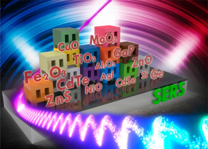
Schematic of semiconductor-enhanced Raman scattering. (Reproduced with permission from ref (8). Copyright 2017, Royal Society of Chemistry.)
To gain a deeper understanding of the CT mechanism, researchers have designed a sandwich structure to observe the CT process between the semiconductor and the probe molecule. Guo et al.15 designed two structures, namely, TiO2–4-mercaptobenzoic acid (MBA)–CdS and CdS–MBA–TiO2, and they have explored the CT process between TiO2 and CdS nanoparticles based on SERS. 4-MBA, which shows clear changes in the Raman intensities and Raman shifts, was employed as the linker and probe molecule between the CdS and TiO2 nanoparticles. For the different systems (TiO2–MBA–CdS and CdS–MBA–TiO2), different CT processes were obtained because of the effect on the dipole moment of an MBA molecule.
The “co-enhancement” phenomenon of the phonon vibration and the probe molecular vibration in semiconductor substrates were studied in terms of the preparation of WO2.72 (W18O49) as the SERS substrate (Figure 2), in which the vibration of the phonon mode and the vibration of the probe molecule after adsorption of the probe molecule were the focus. The phenomenon of “co-enhancement” and the mechanism that leads to this phenomenon have been investigated.16 Due to the Mie scattering resonance effect, submicrometer-sized spherical ZnO superstructures were discovered to provide additional SERS enhancement. This finding offers a new approach to design high-performance SERS-active semiconductor substrates.17
Figure 2.
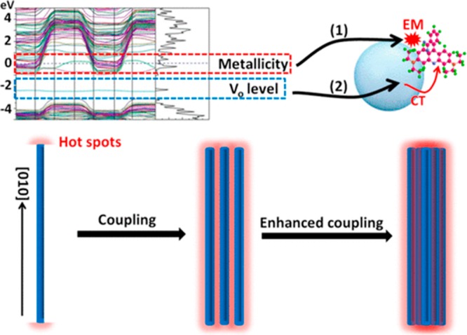
Upper. Band structure of W18O49 and the two possible SERS enhancement methods in W18O49: (1) EM and (2) CT. Lower: LSPR coupling between nanowires. (Reproduced with permission from ref (16). Copyright 2018, American Chemical Society.)
More importantly, with the development of NIR semiconductor materials, many NIR semiconductor materials, such as Cu2–xSe nanoparticles that exhibit NIR SPR, have been used in SERS studies. A plasmon-mediated chemical reaction was observed on Cu2–xSe nanoparticles for the reduction of 4-nitrobenzenethiol to 4,4′-dimercaptoazobenzene based on SERS, which was known to be mediated by the generation of plasmon-derived hot electrons to initiate the multielectron reduction reaction.18
Metal/Semiconductor Composite-Based SERS
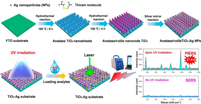
The performance of single nanomaterials has limitations, so composite materials have been developed and have considerable application value. Compared with single nanomaterials, composite materials composed of two or more materials have a greatly improved performance, improved application value, and wider application fields. It is difficult to achieve strong SERS enhancement with simple semiconductor materials. Therefore, the development of precious metal and semiconductor composite materials can expand the theoretical and application development of SERS technology. The design and development of new composite SERS-active substrates are beneficial for theoretical and applied studies on SERS. Precious metals have been compounded with traditional semiconductor materials and have become a hotspot in SERS research due to their relatively simple recovery and excellent performance. In noble metal–semiconductor structures, noble metals exhibit a strong SPR effect in the visible region, which can expand the light absorption. At the same time, noble metals generally have a lower Fermi level than that of semiconductors, and they can promote the separation effect of photogenerated electrons and holes and contribute to the promotion of the CT efficiency between metals. For the novel SERS discoveries, a new material model needs to be developed that places high demands on the design and preparation of materials for applications (Figure 3).19
Figure 3.
Schematic illustration of the synthesis process of anatase nanosheets/rutile nanorod TiO2 heterostructures decorated with AgNP hybrid arrays for photoinduced enhanced Raman spectroscopy detection. (Reproduced with permission from ref (19). Copyright 2019, American Chemical Society.)
Recently, to expand the applicability of SERS, researchers have used metal/semiconductor composites as SERS substrates to observe SERS signals from probe molecules adsorbed on semiconductor surfaces. A series of systems designed to study CMs were designed including Ag/CuO nanocomposites and Ag/4-MPH/TiO2 CT complexes, Au/ZnO/PATP/Ag and TiO2–MBA–Au assemblies, etc.8 In the Cu/ZnO/PATP/Ag assembly,20 it was found that by adjusting the energy level changes reliable experimental conclusions could be drawn based on the SERS spectral differences related to the material properties. When the laser illuminates the system, if the energy levels between the various unit materials match, then for the molecule, a CT resonance effect from the semiconductor to the molecule or from the molecule to the semiconductor is generated, thereby increasing the Raman scattering intensity of the molecule. The prepared substrate can be used not only for preparing highly active SERS substrates for medical detection but also for optical properties, magnetic properties, photodegradation, and solar cell applications.
Researchers have modified the surface of traditional SERS-active materials by modifying the composition of materials, such as SiO2/Al2O3, graphene, and TiO2 semiconductors, to avoid direct contact between the system to be tested and the metal materials.21 The layer interface effect contributes significantly to SERS. SERS is a more versatile and practical method than other methods because this structure can be applied to detect the greatest number of surface chemical components of various materials and substrates with any morphology. Bing Zhao’s group studied the SERS effect by the direct contact interface between the metal and semiconductor (TiO2, ZnO, CuO, etc.) and regulated the CT behavior induced by the metal–semiconductor heterojunctions. This research provides a new strategy for studying the SERS mechanism in metal–semiconductor composite systems.22 The metal–semiconductor heterojunction has the characteristics of improving the visible-light response and the photoexcited electron–hole lifetime. The direct contact interface between the metal and the semiconductor provides an optocoupler interface channel to the system, thereby improving the charge separation efficiency.23 Furthermore, this research establishes a simple and effective way of studying the influence of SPR on interfacial CT by using SERS, which is beneficial for further investigations on interfacial CT.
With the development of nanofabrication technology, layer-by-layer sputtering and cosputtering techniques have been employed to fabricate metal/semiconductor materials on nanoarray templates. Layer-by-layer sputtering of Cu2S and Ag on an array structure has been used in SERS and SPR studies. An enhanced Raman spectrum is obtained using 4-MBA as a probe molecule and exciting with different wavelength excitation lines. This enhancement is due to the combination of excitation transitions and electron-to-semiconductor transitions at certain excitation wavelengths. The study of this composite structure provides a new approach for examining the surface plasmon oscillation regulation and CT mechanism.23 In addition, cosputtering of Ag and Cu2S on a polystyrene (PS) template resulted in an excellent localized surface plasmon resonance (LSPR) that was tunable because of the control of the carrier density of the Ag and Cu2S composite substrates. The LSPR and CT determined by the carrier concentration were investigated by adjusting the semiconductor content. Here, the effect of the controllable carrier concentration on the LSPR and CT in the same system is discussed. By changing the sputtering power of Cu2S in the Ag and Cu2S composite substrates, the LSPR can be easily adjusted from 580 to 743 nm. Surprisingly, the LSPR can be precisely regulated by changing the semiconductor content or even the carrier density. The carrier density is characterized by the Hall effect to analyze the Raman shift caused by CT and to obtain the relationship between them (Figure 4).23
Figure 4.
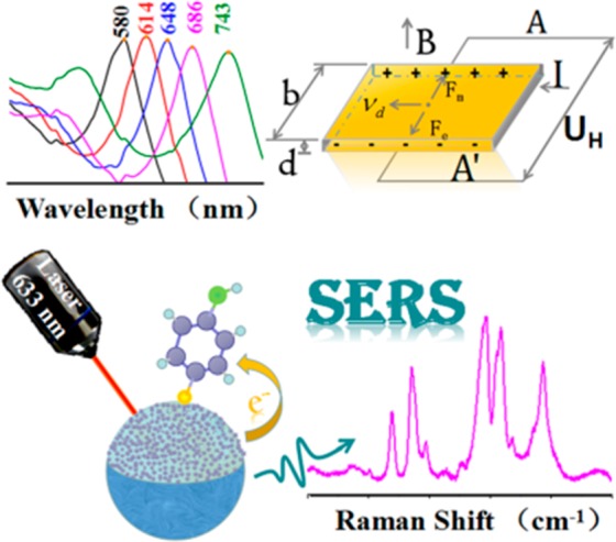
Schematic of the carrier density-dependent localized surface plasmon resonance and CT observed by SERS for the cosputtering of Ag and Cu2S. (Reproduced with permission from ref (23). Copyright 2018, American Chemical Society.)
Organic Semiconductor-Based SERS
Organic films based on small molecular semiconductors (SMSs) offer unique advantages over their inorganic and macromolecular counterparts, including structural versatility, facile and highly controllable synthesis and film fabrication, and fine tuning of optoelectronic properties. With the development of battery materials, researchers have introduced Raman spectroscopy to understand CT processes in battery systems. It was found that organic semiconductor materials also increase the SERS activity and that SERS is a powerful tool for understanding the performance of organic electronic devices.
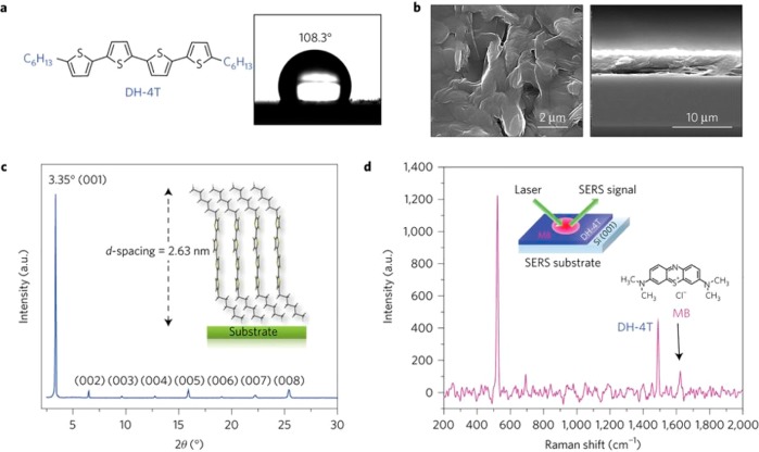
Notably, in 2017, Yilmaz et al. confirmed that the nanoscale organic semiconductor α,ω-diperfluorohexylquaterthiophene (DFH-4T) molecule with hydrophobic properties can significantly enhance the signal of the probe molecule (methylene blue) with an EF of 3.4 × 10³ (Figure 5).24 The SERS enhancement of the proposed pristine organic film is due to the CT between the molecule and the organic substrate. This interpretation is consistent with the resonance description of SERS in that the CT resonance between the molecule and substrate is vibronically coupled to the nearby molecular transition and borrows intensity from it. This discovery provides a new direction for enhanced Raman based on organic semiconductors. At the same time, this effect is precisely why organic semiconductors are often used as electron transport layers or hole transport layers in solar cells. This discovery introduces new ways for studying the carrier dynamics in organic solar cells.
Figure 5.
(a) Chemical structure of DH-4T and the optical image of a water droplet on a 2D DH-4T film used for contact angle measurements. (b,c) Top-view and cross-sectional SEM images (b) and θ–2θ XRD pattern (c) of a 2D DH-4T film (the inset depicts a view of the edge-on molecular orientation with a calculated d-spacing of 2.63 nm along the [001] film growth direction). (d) SERS spectra of methylene blue (MB) on a pristine DH-4T film (the inset shows a schematic representation of the SERS measurement). (Reproduced with permission from ref (24). Copyright 2017, Springer Nature.)
Subsequently, Lombardi24 commented on the work done by Yilmaz et al., with high praise. It has been demonstrated that organic semiconductor films are superior to metal films in terms of stability and reproducibility. Another advantage of organic semiconductor films is the ability to functionally modulate their properties. Coinage metals are similar to a versatile matrix that works for almost any molecule because the Fermi level of the metal lies between the HOMO and the LUMO. The contribution to the CT, coupled with the plasmon resonance, results in a high enhancement. In contrast, the CT between a molecule and a semiconductor substrate involves a semiconductor band edge rather than a Fermi level. The band edge of the semiconductor can be easily adjusted to optimize the CT to specific molecules.
SERS technology is used to study the dynamics of carriers in solar cells. The selection of active substrates is the primary issue for SERS technology. For organic semiconductors commonly used in solar cells, this theory is equally applicable, as reported by Lombardi et al.24 However, unlike inorganic semiconductors, these conductive polymers have a high degree of energy and spatial distribution disorder, so carrier transport can only be from one local state to another. Poly(3,4-ethylenedioxythiophene) polystyrenesulfonate (PEDOT:PSS) is a conjugated conductive polymer with good semiconductor properties. The material can be prepared in solution form at room temperature by various processing methods and is often used as a hole transport layer in solar cells. In the conjugated structure, the overlap of the orbitals leads to the formation of two delocalized states, namely, the LUMO and HOMO. This premise ensures that the CT process in the SERS of organic semiconductors is highly similar to that in the SERS of inorganic semiconductors. Nevertheless, the discussion of organic semiconductors in the enhancement mechanism of SERS is still in its infancy, and the discussion of organic conjugated conductive polymers is currently inactive.25
Another important development is the study of the SERS mechanism by combining organic semiconductors and metal nanoparticles. Stavytska-Barba et al.25 reported poly(3-hexylthiophene)/[6,6]-phenyl-C61-butyric acid methyl ester (P3HT/PCBM) deposited over triangular silver nanoprisms that exhibits excellent SERS enhancement. These nanoprisms have many desirable properties, including large EM enhancement, extensive tunability of a plasmon resonance in the visible spectrum, and self-assembly that does not aggregate on the surface of the silicide glass. In addition, the system demonstrates direct spectral evidence of enhanced charge carrier generation. SERS enhancement can be employed to measure the extent of electromagnetic field enhancement caused by nanoparticles and to examine any changes in Raman spectral properties that may indicate the chemical or morphological effects of the metal on nearby organic materials.
Summary and Outlook
In this review, we outlined a variety of SERS-active inorganic semiconductors, metal/semiconductor composites, and organic semiconductor materials and summarized their basic enhancement mechanism. The main contribution of most semiconductor-based SERS is the CT between the semiconductor and the probe molecule, which improves the SERS enhancement. The theoretical development provides strong support for the practical applications of SERS technology, which demonstrates the great potential for applications of semiconductor-enhanced Raman scattering in solar cells and life science.
Semiconductor SERS substrates have higher SERS uniformity and better chemical stability and biocompatibility compared with those of other types of SERS substrates. In addition, the efficient use of semiconductor SERS substrates may widen the applications of SERS in many fields. Therefore, the design and fabrication of semiconductor materials with high CT efficiency and high EM enhancement will be the basis for SERS applications. However, the selection of SERS-active semiconductor substrates is the primary issue to be addressed. In addition, a small number of molecules were found to be selectively enhanced by semiconductors, which limits the application of semiconductor-based SERS. Direct monitoring of the interfacial chemical reactions of individual nanoparticles remains an enormous challenge. Moreover, the chemical and life science applications of SERS technology are still very limited by SERS-active materials; thus, developing semiconductor materials with high biocompatibility and low biological damage is one of the directions of SERS development. More importantly, due to the high excitation light energy in the visible region, the structure of biological macromolecules is often destroyed. Therefore, developing NIR semiconductor materials with high SERS activity will expand the life science applications of SERS. The field of semiconductor-based SERS will continue to evolve and grow with new developments and successful applications in various scientific areas.
Acknowledgments
This work was supported by the National Research Foundation of Korea (NRF) grants funded by the Korea government (No. NRF-2018R1A2A3074587 and No. NRF-2017K2A9A2A06014372) and Project of Jilin Development and Reform Commission (No. 2019C051-3).
Biographies

Bo Yang received her Masters degree in 2010 at the School of Pharmaceutical Sciences, Changchun University of Chinese Medicine. She joined Prof. Young Mee Jung’s laboratory in July 2018 for 1 month as a Visiting Scholar. Now, she is working as a Research Assistant in Changchun University of Chinese Medicine. Her current research is focused on the SERS-based proteins and medicine study.

Sila Jin received her Masters degree in 2017 at the Department of Chemistry, Kangwon National University. She is a doctoral student under Prof. Young Mee Jung’s supervision at Kangwon National University. Her research focuses on the fabrication of metal/semiconductor SERS-active reusable photocatalysts.

Shuang Guo received her Masters degree at Jilin Normal University in 2019. She joined Prof. Young Mee Jung’s laboratory in August 2019 as a Research Assistant at Kangwon National University. Her research focuses on the construction of nano-semiconductor SERS-active substrates and the study of situ catalytic activity based on SERS.

Yeonju Park received her Doctoral degree under Prof. Young Mee Jung’s supervision from Kangwon National University in 2013. She joined Prof. Young Mee Jung’s laboratory in March 2013 as a postdoctoral fellow, and she is currently a research professor. Her research focuses on vibrational spectroscopy and spectroscopic analysis.

Lei Chen received his Doctoral degree under Prof. Bing Zhao’s supervision from Jilin University in 2011. He joined Prof. Young Mee Jung’s laboratory in October 2011 for 16 months as a postdoctoral fellow of the Brain Korea 21 project. Currently, he works as an associate professor at Jilin Normal University, and his research is focused on the SERS-active nanostructure fabrication and development of SERS-based novel sensing methods for biological analysis.

Bing Zhao received his B.S. degree in 1984 at the Department of Chemistry, Jilin University. Afterward, he went ahead for the graduate studies in the Institute of Theoretical Chemistry at Jilin University and obtained his M.S. and Ph.D. degrees at 1987 and 1992, respectively. In 1992, he joined the chemistry faculty of the state key laboratory of supramolecular structure and materials at Jilin University. In 1998, he was promoted to full professor in the State Key Laboratory of Supramolecular Structure and Materials. His current research is concerned with vibrational spectroscopy and spectroscopic analysis, especially in the field of SERS spectroscopy.

Young Mee Jung is currently a professor of the Department of Chemistry, Kangwon National University, Korea (2005–present). She received her B.S., M.S., as well as Ph.D. in Chemistry from Kyungpook National University, Korea. She was a postdoctoral fellow in Prof. Yukihiro Ozaki’s group at Kwansei Gakuin University, Japan. Her research interest is in the area of spectroscopy, especially SERS and 2D correlation spectroscopy. She chaired the 26th International Conference on Raman Spectroscopy (ICORS) in 2018, Korea. She is currently an Associate Editor of Applied Spectroscopy and on the Editorial Board of both Vibrational Spectroscopy and Spectrochimica Acta A.
Author Contributions
⊥ B.Y. and S.J. contributed equally to this work.
The authors declare no competing financial interest.
References
- Fleischmann M.; Hendra P.J.; McQuillan A.J. Raman spectra of pyridine adsorbed at a silver electrode. Chem. Phys. Lett. 1974, 26, 163–166. 10.1016/0009-2614(74)85388-1. [DOI] [Google Scholar]; Kneipp K.; Ozaki Y.; Tian Z.-Q. Recent Developments in Plasmon-Supported Raman Spectroscopy; World Scientific Publishing Europe Ltd.: London, 2017. [Google Scholar]
- Nie S. M.; Emory S. R. Probing Single Molecules and Single Nanoparticles by Surface-Enhanced Raman Scattering. Science 1997, 275, 1102–1106. 10.1126/science.275.5303.1102. [DOI] [PubMed] [Google Scholar]; Kneipp K.; Wang Y.; Kneipp H.; Perelman L. T.; Itzkan I.; Dasari R. R.; Feld M. S. Single molecule detection using surface-enhanced Raman scattering (SERS). Phys. Rev. Lett. 1997, 78, 1667–1670. 10.1103/PhysRevLett.78.1667. [DOI] [Google Scholar]
- Treffer R.; Böhme R.; Deckert-Gaudig T.; Lau K.; Tiede S.; Lin X.; Deckert V. Advances in TERS (tip-enhanced Raman scattering) for biochemical applications. Biochem. Soc. Trans. 2012, 40, 609–614. 10.1042/BST20120033. [DOI] [PubMed] [Google Scholar]; Han X. X.; Chen L.; Kuhlmann U.; Schulz C.; Weidinger I. M.; Hildebrandt P. Magnetic titanium dioxide nanocomposites for surface-enhanced resonance Raman spectroscopic determination and degradation of toxic anilines and phenols. Angew. Chem., Int. Ed. 2014, 53, 2481–2484. 10.1002/anie.201310123. [DOI] [PubMed] [Google Scholar]; Han X. X.; Zhao B.; Ozaki Y. Label-free detection in biological applications of surface-enhanced Raman scattering. TrAC, Trends Anal. Chem. 2012, 38, 67–78. 10.1016/j.trac.2012.05.006. [DOI] [Google Scholar]
- Zhang R.; Zhang Y.; Dong Z. C.; Jiang S.; Zhang C.; Chen L. G.; Zhang L.; Liao Y.; Aizpurua J.; Luo Y.; Yang J. L.; Hou J. G. Chemical mapping of a single molecule by plasmon-enhanced Raman scattering. Nature 2013, 498, 82–86. 10.1038/nature12151. [DOI] [PubMed] [Google Scholar]; Aroca R.Surface-Enhanced Vibrational Spectroscopy; John Wiley & Sons, Ltd.: Chichester, 2006. [Google Scholar]; Kneipp K.; Moskovits M.; Kneipp H.. Surface-Enhanced Raman Scattering-Physics and Applications; Springer: Berlin, Heidelberg, 2006. [Google Scholar]
- Yamada H.; Yamamoto Y.; Tani N. Surface-enhanced Raman scattering (SERS) of adsorbed molecules on smooth surfaces of metals and a metal oxide. Chem. Phys. Lett. 1982, 86, 397–400. 10.1016/0009-2614(82)83531-8. [DOI] [Google Scholar]; Yamada H.; Yamamoto Y. Surface enhanced Raman scattering (SERS) of chemisorbed species on various kinds of metals and semiconductors. Surf. Sci. 1983, 134, 71–90. 10.1016/0039-6028(83)90312-6. [DOI] [Google Scholar]; Hildebrandt P.; Stockburger M. Surface-enhanced resonance Raman spectroscopy of Rhodamine 6G adsorbed on colloidal silver. J. Phys. Chem. 1984, 88, 5935–5944. 10.1021/j150668a038. [DOI] [Google Scholar]
- Alessandri I.; Lombardi J. R. Enhanced Raman Scattering with Dielectrics. Chem. Rev. 2016, 116, 14921–14981. 10.1021/acs.chemrev.6b00365. [DOI] [PubMed] [Google Scholar]
- Ji W.; Song W.; Tanabe I.; Wang Y.; Zhao B.; Ozaki Y. Semiconductor-enhanced Raman scattering for highly robust SERS sensing: the case of phosphate analysis. Chem. Commun. 2015, 51, 7641–7644. 10.1039/C5CC02395E. [DOI] [PubMed] [Google Scholar]; Ji W.; Wang Y.; Tanabe I.; Han X. X.; Zhao B.; Ozaki Y. Semiconductor-driven “turn-off” surface-enhanced Raman scattering spectroscopy: application in selective determination of chromium(VI) in water. Chem. Sci. 2015, 6, 342–348. 10.1039/C4SC02618G. [DOI] [PMC free article] [PubMed] [Google Scholar]; Wang Y.; Ruan W.; Zhang J.; Yang B.; Xu W.; Zhao B.; Lombardi J. R. Direct Observation of Surface-Enhanced Raman Scattering in ZnO Nanocrystals. J. Raman Spectrosc. 2009, 40, 1072–1077. 10.1002/jrs.2241. [DOI] [Google Scholar]
- Han X. X.; Ji W.; Zhao B.; Ozaki Y. Semiconductor-enhanced Raman scattering: active nanomaterials and applications. Nanoscale 2017, 9, 4847–4861. 10.1039/C6NR08693D. [DOI] [PubMed] [Google Scholar]
- Jiang X.; Song K.; Li X.; Yang M.; Han X.; Yang L.; Zhao B. Double Metal Co-Doping of TiO2 Nanoparticles for Improvement of their SERS Activity and Ultrasensitive Detection of Enrofloxacin: Regulation Strategy of Energy Levels. Chemistryselect 2017, 2 (10), 3099–3105. 10.1002/slct.201700099. [DOI] [Google Scholar]
- Gao Y.; Gao N.; Li H.; Yuan X.; Wang Q.; Cheng S.; Liu J. Semiconductor SERS of diamond. Nanoscale 2018, 10, 15788–15792. 10.1039/C8NR04465A. [DOI] [PubMed] [Google Scholar]
- Zheng Z.; Cong S.; Gong W.; Xuan J.; Li G.; Lu W.; Geng F.; Zhao Z. Semiconductor SERS enhancement enabled by oxygen incorporation. Nat. Commun. 2017, 8, 1993. 10.1038/s41467-017-02166-z. [DOI] [PMC free article] [PubMed] [Google Scholar]
- Yang L.; Peng Y.; Yang Y.; Liu J.; Huang H.; Yu B.; Zhao J.; Lu Y.; Huang Z.; Li Z.; Lombardi J. R. A Novel Ultra-Sensitive Semiconductor SERS Substrate Boosted by the Coupled Resonance Effect. Adv. Sci. 2019, 6, 1900310. 10.1002/advs.201900310. [DOI] [PMC free article] [PubMed] [Google Scholar]
- Ling X.; Moura L. G.; Pimenta M. A.; Zhang J. Charge-Transfer Mechanism in Graphene-Enhanced Raman Scattering. J. Phys. Chem. C 2012, 116, 25112–25118. 10.1021/jp3088447. [DOI] [Google Scholar]; Tan Y.; Ma L.; Gao Z.; Chen M.; Chen F. Two-Dimensional Heterostructure as a Platform for Surface-Enhanced Raman Scattering. Nano Lett. 2017, 17, 2621–2626. 10.1021/acs.nanolett.7b00412. [DOI] [PubMed] [Google Scholar]; Yin Y.; Miao P.; Zhang Y.; Han J.; Zhang X.; Gong Y.; Gu L.; Xu C.; Yao T.; Xu P.; Wang Y.; Song B.; Jin S. Significantly Increased Raman Enhancement on MoX2 (X = S, Se) Monolayers Upon Phase Transition. Adv. Funct. Mater. 2017, 27, 1606694. 10.1002/adfm.201606694. [DOI] [Google Scholar]; Lin J. J.; Liang L. B.; Ling X.; Zhang S. Q.; Mao N. N.; Zhang N.; Sumpter B. G.; Meunier V.; Tong L. M.; Zhang J. Enhanced Raman Scattering on In-Plane Anisotropic Layered Materials. J. Am. Chem. Soc. 2015, 137, 15511–15517. 10.1021/jacs.5b10144. [DOI] [PubMed] [Google Scholar]
- Miao P.; Qin J. K.; Shen Y.; Su H.; Dai J.; Song B.; Du Y.; Sun M.; Zhang W.; Wang H. L.; Xu C. Y.; Xu P. Unraveling the Raman Enhancement Mechanism on 1T-Phase ReS2 Nanosheets. Small 2018, 14, 1704079. 10.1002/smll.201704079. [DOI] [PubMed] [Google Scholar]
- Guo L.; Zhang X.; Li P.; Han R.; Liu Y.; Han X.; Zhao B. Surface-enhanced Raman scattering (SERS) as a probe for detection of charge-transfer between TiO2 and CdS nanoparticles. New J. Chem. 2019, 43, 230–237. 10.1039/C8NJ04003F. [DOI] [Google Scholar]
- Liu W.; Bai H.; Li X.; Li W.; Zhai J.; Li J.; Xi G. Improved Surface-Enhanced Raman Spectroscopy Sensitivity on Metallic Tungsten Oxide by the Synergistic Effect of Surface Plasmon Resonance Coupling and Charge Transfer. J. Phys. Chem. Lett. 2018, 9, 4096–4100. 10.1021/acs.jpclett.8b01624. [DOI] [PubMed] [Google Scholar]
- Ji W.; Li L.; Song W.; Wang X.; Zhao B.; Ozaki Y. Enhanced Raman Scattering by ZnO Superstructures: Synergistic Effect of Charge Transfer and Mie Resonances. Angew. Chem., Int. Ed. 2019, 58, 14552–14556. [DOI] [PubMed] [Google Scholar]
- Gan X. Y.; Keller E. L.; Warkentin C. L.; Crawford S. E.; Frontiera R. R.; Millstone J. E. Plasmon-Enhanced Chemical Conversion Using Copper Selenide Nanoparticles. Nano Lett. 2019, 19, 2384–2388. 10.1021/acs.nanolett.8b05088. [DOI] [PubMed] [Google Scholar]
- Zhang M.; Sun H.; Chen X.; Yang J.; Shi L.; Chen T.; Bao Z.; Liu J.; Wu Y. Highly Efficient Photoinduced Enhanced Raman Spectroscopy (PIERS) from Plasmonic Nanoparticles Decorated 3D Semiconductor Arrays for Ultrasensitive, Portable, and Recyclable Detection of Organic Pollutants. ACS Sens. 2019, 4, 1670–1681. 10.1021/acssensors.9b00562. [DOI] [PubMed] [Google Scholar]
- Mao Z.; Song W.; Xue X.; Ji W.; Chen L.; Lombardi J. R.; Zhao B. Multiphonon Resonant Raman Scattering and Photoinduced Charge-Transfer Effects at ZnO–Molecule Interfaces. J. Phys. Chem. C 2012, 116, 26908–26918. 10.1021/jp3092573. [DOI] [Google Scholar]
- Li J. F.; Huang Y. F.; Ding Y.; Yang Z. L.; Li S. B.; Zhou X. S.; Fan F. R.; Zhang W.; Zhou Z. Y.; Wu D. Y.; Ren B.; Wang Z. L.; Tian Z. Q. Shell-isolated nanoparticle-enhanced Raman spectroscopy. Nature 2010, 464, 392–395. 10.1038/nature08907. [DOI] [PubMed] [Google Scholar]
- Wang Y.; Liu J.; Ozaki Y.; Xu Z.; Zhao B. Effect of TiO2 on Altering Direction of Interfacial Charge Transfer in a TiO2-Ag-MPY-FePc System by SERS. Angew. Chem., Int. Ed. 2019, 58, 8172–8176. 10.1002/anie.201900589. [DOI] [PubMed] [Google Scholar]; Ji W.; Xue X.; Ruan W.; Wang C.; Ji N.; Chen L.; Li Z.; Song W.; Zhao B.; Lombardi J. R. Scanned chemical enhancement of surface-enhanced Raman scattering using a charge-transfer complex. Chem. Commun. 2011, 47, 2426–2428. 10.1039/C0CC03697H. [DOI] [PubMed] [Google Scholar]
- Zhang X.-Y.; Han D.; Pang Z.; Sun Y.; Wang Y.; Zhang Y.; Yang J.; Chen L. Charge Transfer in an Ordered Ag/Cu2S/4-MBA System Based on Surface-Enhanced Raman Scattering. J. Phys. Chem. C 2018, 122, 5599–5605. 10.1021/acs.jpcc.8b00701. [DOI] [Google Scholar]; Zhang X.-Y.; Han D.; Ma N.; Gao R.; Zhu A.; Guo S.; Zhang Y.; Wang Y.; Yang J.; Chen L. Carrier Density-Dependent Localized Surface Plasmon Resonance and Charge Transfer Observed by Controllable Semiconductor Content. J. Phys. Chem. Lett. 2018, 9, 6047–6051. 10.1021/acs.jpclett.8b02416. [DOI] [PubMed] [Google Scholar]
- Yilmaz M.; Babur E.; Ozdemir M.; Gieseking R. L.; Dede Y.; Tamer U.; Schatz G. C.; Facchetti A.; Usta H.; Demirel G. Nanostructured organic semiconductor films for molecular detection with surface-enhanced Raman spectroscopy. Nat. Mater. 2017, 16, 918–925. 10.1038/nmat4957. [DOI] [PubMed] [Google Scholar]; Lombardi J. R. Enhanced by organic surface. Nat. Mater. 2017, 16, 878–880. 10.1038/nmat4958. [DOI] [PubMed] [Google Scholar]
- Razzell-Hollis J.; Thiburce Q.; Tsoi W. C.; Kim J.-S. Interfacial Chemical Composition and Molecular Order in Organic Photovoltaic Blend Thin Films Probed by Surface-Enhanced Raman Spectroscopy. ACS Appl. Mater. Interfaces 2016, 8 (45), 31469–31481. 10.1021/acsami.6b12124. [DOI] [PubMed] [Google Scholar]; Stavytska-Barba M.; Salvador M.; Kulkarni A.; Ginger D. S.; Kelley A. M. Plasmonic Enhancement of Raman Scattering from the Organic Solar Cell Material P3HT/PCBM by Triangular Silver Nanoprisms. J. Phys. Chem. C 2011, 115, 20788–20794. 10.1021/jp206853u. [DOI] [Google Scholar]


