Abstract
In2O3 nanoparticle (NP)-decorated WO3 nanorods (NRs) were prepared using sol–gel and hydrothermal methods. The In2O3 NRs and WO3 NPs were crystalline. WO3 NP-decorated In2O3 NRs were also prepared using thermal evaporation and hydrothermal methods. The NO2 sensing performance of the In2O3 NP-decorated WO3 NR sensor toward NO2 was compared to that of the WO3 NP-decorated In2O3 NR sensor. The former showed a high response to NO2 due to a significant reduction of the conduction channel width upon exposure to NO2. In contrast, the latter showed a far less pronounced response due to limited reduction of the conduction channel width upon exposure to NO2. When the sensors were exposed to a reducing gas instead of an oxidizing gas (NO2), the situation was reversed, i.e., the WO3 NP-decorated In2O3 NR exhibited a stronger response to the reducing gas than the In2O3 NP-decorated WO3 NR sensor. Thus, a semiconducting metal oxide (SMO) with a smaller work function must be used as the decorating material in decorated heterostructured SMO sensors for detection of oxidizing gases. The In2O3 NP-decorated WO3 NR sensor showed higher selectivity for NO2 compared to other gases, including reducing gases and other oxidizing gases, as well as showed high sensitivity to NO2.
Keywords: Gas sensor, Heterostructure, WO3, In2O3, NO2
Introduction
Despite the numerous merits of semiconducting metal oxides (SMOs) as sensor materials there are still certain limitations, such as their relatively low response to gases at room temperature and dissatisfactory selectivity [1]. To address the dissatisfactory sensing properties, various strategies have been attempted, including noble metal catalyst doping, heterojunction formation, and radiation-assisted treatment with energetic particles including ion beams, electrons, and ultraviolet (UV) lights [2–4]. Of these techniques, heterostructure formation is plausibly most widely studied and is used for the fabrication of chemiresistive nanostructured gas sensors. There are several types of heterostructures including p-n, n–n and p–p heterostructures. Generally, p–p heterostructures are less commonly utilized because of their inferior sensing properties, whereas n–n heterostructures are as widely utilized as the p–n counterparts because of their superior sensing properties [5]. However, strangely, n–n heterostructures have not been studied as intensively as the p–n congeners. The enhanced sensing properties of n–n heterostructures are mainly due to the resistance modulation at the n–n heterojunctions in n–n heterostructures. Various heterostructure combinations are known, such as a simple mixture of two different types of n-SMOs [6], bi-layer type n–n nanostructures [7], n–n core–shell structures [8], a single type of n-SMO nanostructure decorated with another type of n-SMO nanoparticles (NPs) [9], etc.
This study focuses on, decorated n–n heterostructures. WO3 and In2O3 are chosen as sensor materials for detecting a typical oxidizing gas, NO2. The sensing properties of In2O3 NP-decorated WO3 nanorods (NRs), WO3 NP-decorated In2O3 NRs, pristine WO3 NRs, and pristine In2O3 NRs are compared and the differences in the sensing properties of these four nanostructures are analyzed and the origin of the differences is discussed in detail.
Methods
Preparation of In2O3 nanoparticles-decorated WO3 nanorods
High purity In2O3 NPs were synthesized using a sol–gel method [10]. Indium acetate ([In(C2H3O2)2·H2O]; 0.6695 g) was dissolved in diethylene glycol and stirred for 5 min. The solution was homogenized by heating to 130 °C and 3 mL of 3 N-nitric acid was added to the solution and stirred well. The solution was heated at 180 °C for 5 h, and pure yellowish In2O3 NPs were precipitated. The In2O3 NPs were dried at 400 °C for 2 h and then calcined at 500 °C for 1 h to obtain the pure In2O3 NPs. The WO3 NRs were synthesized by using a low-temperature hydrothermal method [11]. Sodium tungstate (1.956 mL) and oxalic acid (1.512 mL) were dissolved in distilled water (50 mL). The solution was acidified to PH 0.7–0.9 by mixing with 3 mol/L HCl solution. A transparent precursor solution was formed and 3 g of K2SO4 was added to the solution. The mixed solution was maintained in an autoclave at 100 °C for 24 h, cooled to room temperature, and was centrifuged to collect the green product. The product was rinsed with ethanol and dried at 60 °C for 1 h to obtain pure WO3 NRs. The substrate on which the WO3 NRs were synthesized was placed on a spin coater and then rotated at 500 rpm. The In2O3 NPs synthesized via the sol–gel method were dispersed in ethanol with a micropipette and the ethanolic dispersion of In2O3 NPs was dropped on the rotating WO3 NR substrate.
Preparation of WO3 nanoparticles-decorated In2O3 nanorods
In2O3 NRs were synthesized using a thermal evaporation method [12]. A 3 mm thick gold film—coated p-type Si (100) substrate was placed on the top of an alumina boat containing a mixture of In2O3 powders and positioned at the center of a horizontal quartz tube furnace. The furnace was heated to 900 °C and maintained at that temperature for 30 min under argon gas at a constant flow rate of 200 cm3/min. The WO3 NPs were synthesized using a hydrothermal method [13]. WO3 powders (2 mL) were dissolved in 48 mL of hydrochloric acid in sonicater. The pH of the solution was controlled at 7 using sodium hydroxide. After sonication of the solution for 6 h the precipitated powders were collected by removing the liquid, leaving the powders behind. The powders were placed into a hydrothermal synthesizer containing ethanol and the synthesizer was placed in an oven and heated at 180 °C for 12 h. WO3 NPs were synthesized in the hydrothermal synthesizer. The substrate on which the In2O3 NRs were synthesized by the thermal evaporation method was placed in a beaker containing ethanol and then ultrasonicated to separate the In2O3 NRs from the substrate. Meanwhile, the WO3 NPs synthesized by the hydrothermal method were dispersed in ethanol. The two solutions (In2O3 NRs dispersed in ethanol and the WO3 NPs dispersed in ethanol) were mixed and the mixed solution was exposed to UV (254 nm) irradiation for 12 h using a UV lamp. The mixed solution was then annealed under argon atmosphere at 400 °C for 1 h in an annealing furnace.
Fabrication of chemiresistive sensors
The In2O3 NP-decorated WO3 NRs and WO3 NP-decorated In2O3 NRs grown on the Si substrate were dispersed ultrasonically in isopropyl alcohol. A multiple-networked chemiresistive sensor was fabricated by pouring the solution containing the precursors of the two different nanostructures onto SiO2/Si substrates with a patterned interdigital electrode with a double layer comprising separate layers of Ti (10 nm) and Au (100 nm): the assembly was dried at 150 °C for 1 min. For comparison of the sensing properties, pristine In2O3 and WO3 NR sensors were also fabricated in a similar manner.
Characterization
The microstructures and phases of the synthesized NR samples were examined by scanning electron microscopy (SEM) and X-ray diffraction (XRD), respectively. The microstructures and phases of the samples were examined further by transmission electron microscopy (TEM).
Gas sensing tests
The NO2 sensing performances of the fabricated sensors were examined using a custom-made gas sensing system. The concentration of NO2 gas was controlled precisely in the concentration range of 5–200 ppm by mixing NO2 with dry synthetic air using the mass flow controllers. Electrical measurements to examine the sensing properties of the sensors were conducted at room temperature under 50% relative humidity. The detailed sensing test procedure is described elsewhere [14]. The response of the sensors to NO2 was evaluated by using the Rg/Ra ratio, where Rg and Ra are the resistances of the sensor measured in the presence of air and NO2, respectively. The response and recovery times were determined by measuring the times required to reach 90% of the total change in the resistance of the sensor after exposure of the sensor to the analyte gas and ambient air, respectively.
Results and discussion
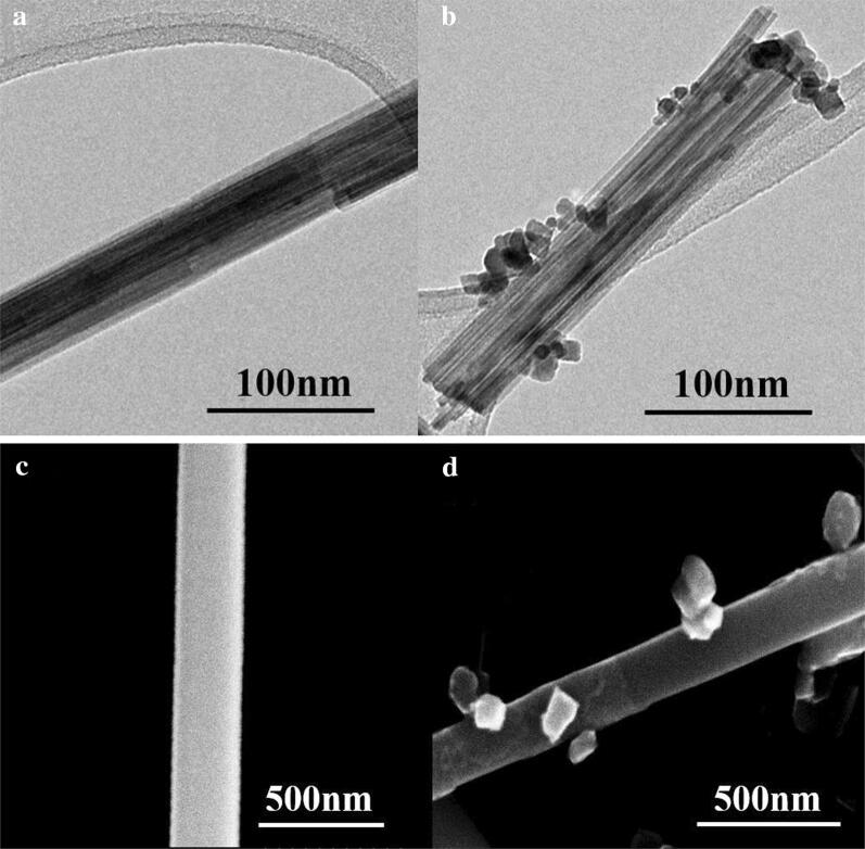
Figure 1a, b show low-magnification TEM images of the pristine and In2O3 NPs-decorated WO3 NRs, respectively. The average diameter of the WO3 NRs was ~ 50 nm and the length of the WO3 NRs ranged from 200 to 1100 nm. The average diameter of the In2O3 NPs on the WO3 NRs was 20 nm. The SEM images of the pristine and WO3 NP-decorated In2O3 NRs are exhibited in Fig. 1c, d. The average diameter of the In2O3 NRs was 250 nm and the lengths of the In2O3 NRs ranged from 1 to 10 μm. The average diameter of the WO3 NPs on the In2O3 NRs was 140 nm. Hence, the average diameter of the WO3 NPs on the In2O3 NRs was ~ 7 times larger than that of the In2O3 NPs on the WO3 NRs. The difference in size might be due to the different preparation methods (sol–gel versus hydrothermal methods).
Fig. 1.
Low-magnification TEM images: a pristine and b In2O3 NPs-decorated WO3 NRs and SEM images: c pristine and d WO3 NPs-decorated In2O3 NRs
Figure 2a, b show the XRD patterns of the In2O3 NP-decorated WO3 NRs and WO3 NP-decorated In2O3 NRs, respectively. In the former pattern, the WO3 NRs exhibited relatively sharp and intense reflection peaks, assigned to the primitive tetragonal structured WO3 (JCPDS card No. 89-4481, a = 0.5275 nm, c = 0.7846 nm). In contrast, the In2O3 NPs exhibited relatively less sharp and less intense reflection peaks, assigned to body-centered cubic In2O3 with a lattice constant of a = 1.011 nm (JCPDS No. 89-4595). The lower intensity peaks for In2O3 compared to WO3 might be due to the smaller volume of the In2O3 NPs relative to that of the WO3 NRs. In contrast, in the latter pattern (Fig. 2b), In2O3 peaks were taller and sharper than WO3 peaks, which might be due to the larger volume of In2O3 NRs than those of the WO3 NPs.
Fig. 2.
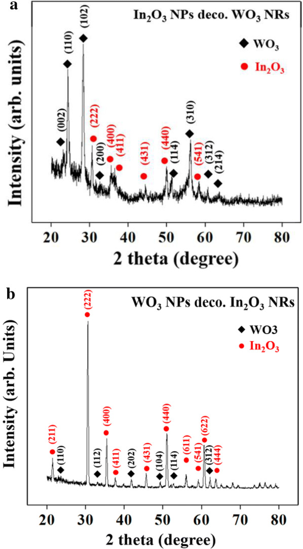
XRD patterns of a In2O3 NPs-decorated WO3 NRs and b WO3 NPs-decorated In2O3 NRs
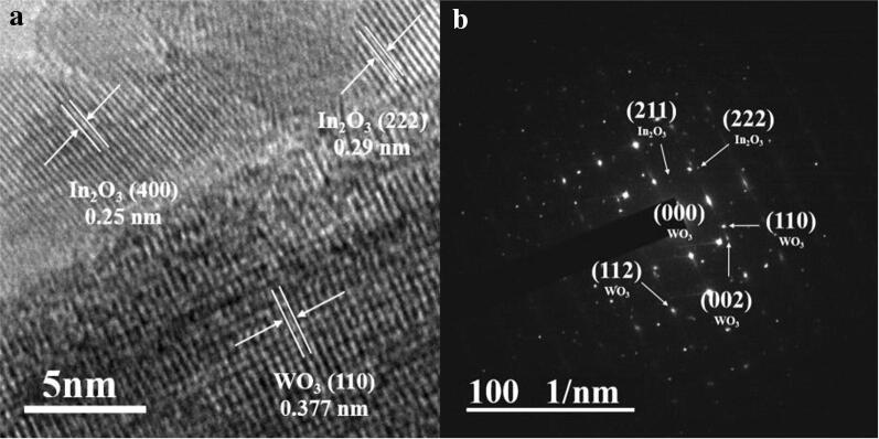
Figure 3a, b present the high-resolution TEM image and corresponding selected area electron diffraction (SAED) pattern of the In2O3 NP-decorated WO3 NRs. The regularly aligned fringes in both the WO3 and In2O3 regions suggest that the WO3 and In2O3 nanostructures are both crystalline. The corresponding spotty electron diffraction (ED) pattern in Fig. 3b reveals that the WO3 and In2O3 nanostructures are single crystals.
Fig. 3.
a High-resolution TEM image, b corresponding electron diffraction pattern of the In2O3 NPs-decorated WO3 NRs
The temperature-dependent responses of all four different sensor materials to NO2 are presented in Fig. 4. The responses of all the four sensor materials to NO2 tended to increase with increasing temperature up to 300 °C, and then to decrease with further increases in the temperature. This result suggests that 300 °C is the optimal operating temperature of the sensors in detecting the NO2. All the sensing tests hereafter were conducted at 300 °C. At too low operating temperature (250 °C or lower), the NO2 molecules may not have enough energy to overcome the energy barrier of adsorption, and fail to be adsorbed on the surface of the sensor materials, WO3 and In2O3. However, at too high operating temperature (350 °C or higher), adsorption failure might also occur because the rate of desorption may outweigh that of adsorption [15].
Fig. 4.
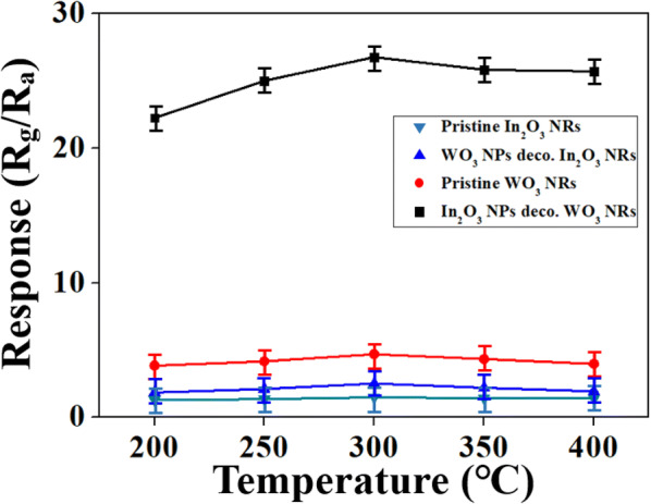
Responses of In2O3 NPs-decorated WO3 NRs and WO3 NPs-decorated In2O3 NPs along with pristine WO3 NRs and pristine WO3 NRs at various operating temperatures to NO2
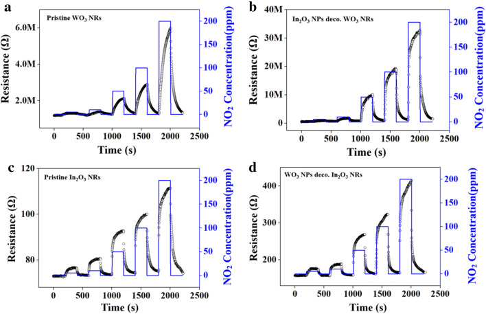
Figure 5a–d present the dynamic response curves of the four different sensors toward NO2. All the sensors showed stable and reversible response and recovery behavior. The resistances of the sensors increased when an oxidizing gas (NO2) was supplied, and recovered to the initial value when the NO2 supply was stopped and the sensors were exposed to ambient air. This response toward the oxidizing gas is in accord with the sensing behavior of n-type semiconductors. As is well known, both WO3 and In2O3 are n-type semiconductors. The resistance changes increased as the NO2 concentration was increased. The starting resistances of the pristine and WO3 NP-decorated In2O3 NRs was markedly lower than the pristine and In2O3 NPs-decorated WO3 NRs, respectively, which might be due to the much lower resistivity of In2O3 than that of WO3.
Fig. 5.
Dynamic response curves: a pristine WO3 NRs to NO2, b In2O3 NPs-decorated WO3 NRs to NO2, c pristine In2O3 NRs to NO2, and d WO3 NPs-decorated In2O3 NRs to NO2
Figure 6 shows the responses of the four different sensors to NO2 as a function of the NO2 concentration. The response of the In2O3 NP-decorated WO3 NRs to NO2 far exceeded those of the other three sensors over the entire NO2 concentration range. The more pronounced response of the In2O3 NP-decorated WO3 NR sensor to NO2 than that of the pristine WO3 NRs and the greater response of the WO3 NPs-decorated In2O3 NRs sensor to NO2 than that of the pristine In2O3 NRs is plausibly due to the resistance modulation at the WO3–In2O3 heterojunction formation [16]. Contrarily, the much stronger response of the In2O3 NP-decorated WO3 NR sensor to NO2 than that of the WO3 NP-decorated In2O3 NR sensor is very interesting. The origin of this difference in the response of the heterostructured sensors with inverse configuration is discussed in detail in the next section.
Fig. 6.
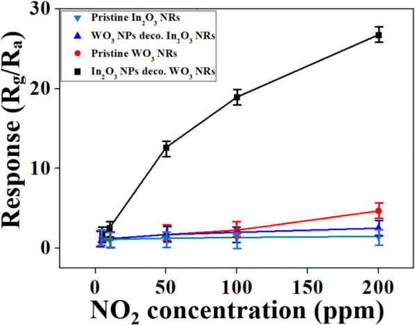
Calibration curves for responses of pristine and In2O3 NPs-decorated WO3 to NO2 as well as those of pristine and WO3 NPs-decorated In2O3 NRs to NO2 as a function of NO2 concentrations
Figure 7a, b show the response and recovery times of the four different sensors toward NO2 as a function of the NO2 concentration. As expected, the response and recovery times of the In2O3 NP-decorated WO3 NR sensor were shorter than those of the pristine WO3 NRs. In contrast, the response and recovery times of the WO3 NP-decorated In2O3 NR sensor were longer than those of the pristine In2O3 NR sensor. Comparison of the response and recovery times of the In2O3 NP-decorated WO3 NR sensor with those of the WO3 NP-decorated In2O3 NR sensor, interestingly, shows shorter response and recovery times for the former in the higher NO2 concentration range, whereas longer response and recovery times for the lower NO2 concentration range than the latter. Shorter response and recovery times are commonly associated with a higher response for gas sensors.
Fig. 7.
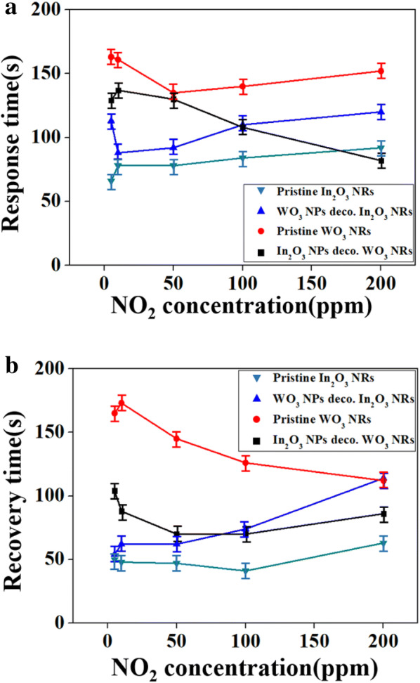
Calibration curves for a response times and b recovery times of pristine and In2O3 NPs-decorated WO3 NRs as well as pristine and WO3 NPs-decorated In2O3 NRs to NO2 as a function of NO2 concentrations
The response of the In2O3 NP-decorated WO3 NR sensor to various gases is shown in Fig. 8. The sensor showed a much stronger response to NO2 than to the other oxidizing gases such as O3 and SO2 or reducing gases such as CO, CH4 and H2S, demonstrating the selectivity and sensitivity of the In2O3 NP-decorated WO3 NR sensor toward NO2. The selectivity of the sensor toward NO2 against other gases might be related to the different optimal operating temperatures of the sensor for different target gases. The response of a sensor material to a certain gas might depend on many factors such as solid solubility of the gas in the material, the decomposition rate of the adsorbed molecule at the material surface, the charge carrier concentration in the material, the Debye length in the material, the catalytic activity of the material, the orbital energy of the gas molecule, etc. The dissociation (or reduction) rate of an oxidizing gas such as NO2 is determined by these factors. Therefore, each gas has the characteristic optimal dissociation temperature at which its dissociation rate is maximized. The In2O3-decorated WO3 nanorod sensor fabricated in this study showed higher response fortunately to NO2 than other gases at 300 °C because of the higher dissociation rate of NO2 at the surface of In2O3 and WO3 at the temperature, but it might show higher responses to other gases than NO2 at different temperatures [17–22].
Fig. 8.
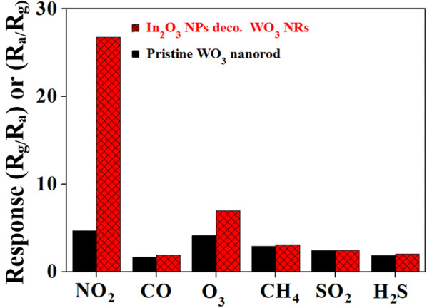
Selectivity patterns of pristine and In2O3 NPs-decorated WO3 NRs toward NO2 against other gases such as O3, SO2, CO, CH4, and H2S
Figure 9a–d illustrate the sensing mechanism of the In2O3 NP-decorated WO3 NR sensor toward NO2. Earlier studies reported that the response of a base sensor material could be enhanced by decoration with another type of SMO NPs, mainly because of the greater modulation of the width of the depletion layer or the conduction channel, resulting in the greater modulation of the sensor resistance [23–25]. n-Type WO3 has a larger work function (qΦ) than n-type In2O3 (Fig. 9a). Accordingly, if WO3 and In2O3 are in contact, even under vacuum, electron transfer from In2O3 (with a larger work function) to WO3 (with a smaller work function) tends to occur until electronic equilibrium is attained between WO3 and In2O3, as shown in Fig. 9a. Consequently, electron-accumulation and electron-depletion layers are formed in the WO3 and In2O3 regions, respectively. The schematic shows the In2O3 NP-decorated WO3 NRs with an accumulation layer with a width of W11, formed by electron transfer from the In2O3 NPs to the WO3 NRs (Fig. 9b). In ambient air, the surfaces of the WO3 NR and In2O3 NP adsorb oxygen molecules and the adsorbed oxygen molecules are ionized by the capture of the free electrons in the WO3 and In2O3 surface regions (Fig. 9c). Consequently, a depletion layer with a width of W12 is formed in the surface region of WO3. The schematic shows a decorated WO3 NR with a depletion layer formed via ionization of adsorbed oxygen molecules and an accumulation layer formed by electron transfer from the In2O3 to the WO3 (Fig. 9c). When NO2 gas is supplied, NO2 and O2 molecules are both adsorbed by the In2O3 and WO3 surfaces. The adsorbed NO2 molecules are converted into NO2− or NO [26, 27] and the adsorbed oxygen molecules are converted into oxygen ions by capturing electrons from the WO3 and In2O3 surface regions. Consequently, a thicker depletion layer (with a width of W22) (Fig. 9d) is formed than that formed in ambient air. The schematic shows a WO3 NR with a depletion layer with a width of W22 as well as the accumulation layer with a width of W21 formed by the electron transfer from the In2O3 to the WO3 (Fig. 9d).
Fig. 9.
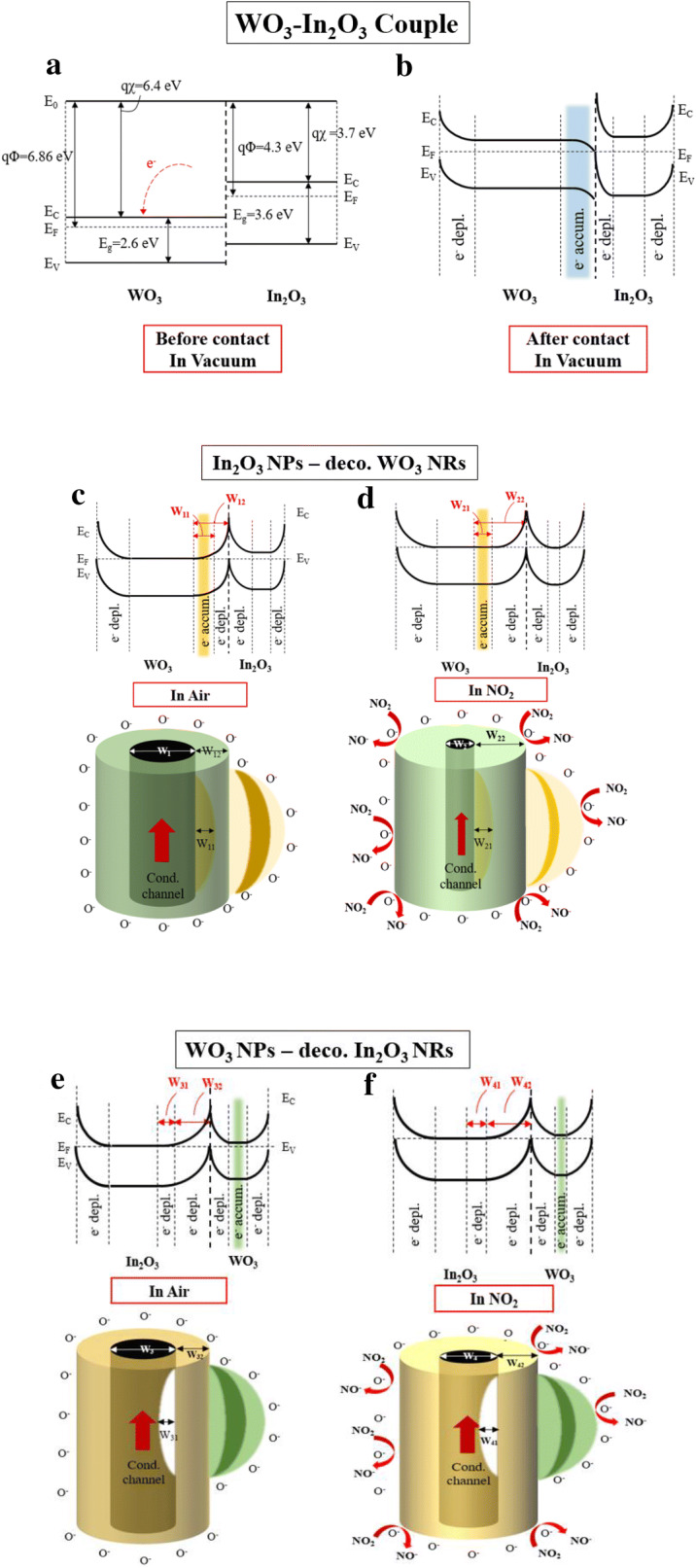
Energy band diagrams of a WO3-In2O3 couple a before and b after contact. Energy band diagrams and schematics of In2O3 NPs-decorated WO3 NRs: c in air and d in NO2, and of WO3 NPs-decorated In2O3 NRs: e in air and f in NO2
The sensing mechanism of the WO3 NP-decorated In2O3 NR sensor toward NO2 is illustrated in Fig. 9e, f. As discussed above, electron-accumulation and depletion layers are formed in the WO3 and In2O3 regions, respectively. Thus, a depletion layer with a width of W31 forms on the In2O3 side of the WO3–In2O3 interface (Fig. 9e). In ambient air, oxygen molecules are adsorbed by the In2O3 NR surface and ionized by accepting the electrons from the In2O3 and WO3 surface regions. Consequently, a depletion layer with a width of W32 is formed in the In2O3 surface region. A WO3 NP-decorated In2O3 NR with a depletion layer formed due to the ionization of adsorbed oxygen molecules and a depletion layer formed by electron transfer from the WO3 NP is shown in Fig. 9e. Under NO2 atmosphere, a thicker depletion layer (with a width of W42) than that generated in ambient air is formed due to the adsorption and ionization of both NO2 and O2 molecules (Fig. 9f). Note that no electron-accumulation layer is formed in the In2O3 NR throughout the on–off cycling of the NO2 gas supply.
Under ambient air and NO2, there was no big difference in the basic response of the In2O3 NPs-decorated WO3 NRs versus that of the WO3 NPs-decorated In2O3 NRs. A relatively thin depletion layer is formed in both samples upon exposure to air and a thick depletion layer is generated upon exposure to NO2. Consequently, the width of the conduction channel of the In2O3 NP-decorated WO3 NRs formed upon exposure to NO2 is much smaller than that of the WO3 NP-decorated In2O3 NRs formed in ambient air. The conduction channel of the In2O3 NP-decorated WO3 NRs has a room for substantial reduction upon exposure to NO2 because the conduction channel width has already been expanded due to the formation of an accumulation layer by the transfer of electrons from the In2O3 NP to the WO3 NR. In contrast, the conduction channel of the WO3 NPs-decorated In2O3 NRs was already shrunken due to the formation of the electron-depletion layer via electron transfer from the In2O3 NR to the WO3 NP. Accordingly, the conduction channel of the In2O3 NR has little room for further reduction upon exposure to NO2 [28].
The response, S is defined as Rg/Ra. for the oxidizing gas NO2 and S is proportional to Aa/Ag because the resistance R = ρl/A, where ρ, l and A are the density, length and cross-sectional area of the conductor (channel, here) [29]. S can be expressed as the ratio of the conduction channel width for an analyte gas to that for air, S = W2a/W2g because A = πW2, where W is the conduction channel width. Therefore, the In2O3 NP-decorated WO3 NR sensor has a higher response, S to NO2 because of the far smaller conduction channel width, Wg in NO2 atmosphere. In contrast, the WO3 NP-decorated In2O3 NR sensor has a lower response, S because of the lower contraction of the conduction channel width, Wg in NO2 atmosphere.
Conclusions
The sensing properties of the In2O3 NP-decorated WO3 NR sensor toward NO2 were compared to those of the WO3 NP-decorated In2O3 NR sensor. The response of the former sensor to NO2 was more pronounced than that of the latter due to the significant reduction of the conduction channel width of the former sensor upon exposure to NO2. The conduction channel of the In2O3 NP-decorated WO3 NR sensor had room for sufficient reduction as it was already expanded by electron transfer from the In2O3 NPs to the WO3 NRs. In contrast, the WO3 NP-decorated In2O3 NR sensor showed a lower response due to insufficient reduction of the conduction channel width upon exposure to NO2. The conduction channel of the WO3 NP-decorated In2O3 NR sensor had little room for further reduction due to prior shrinkage associated with electron transfer from the In2O3 NRs to the WO3 NPs. For the detection of a reducing gas instead of an oxidizing gas, the magnitude of the sensor response would be reversed. Therefore, choosing a proper decorating material in fabricating n-SMO NR sensors decorated with n-SMO NPs is important in obtaining high sensitivity. An SMO with a smaller work function must be chosen as a decorating material in a decorated heterostructured sensor for oxidizing gas detection. In contrast, an SMO with a larger work function must be chosen as the decorating material for heterostructured sensors geared toward the detection of a reducing gas.
Acknowledgements
This work was supported by the National Research Foundation of Korea grant funded by the Korea government (MSIT), South Korea (No. 2017R1A2B4010034) and Basic Science Research Program through the National Research Foundation of Korea (NRF) funded by the Ministry of Education, South Korea (No.2016R1A6A3A11934765).
Abbreviations
- NP
nanoparticle
- NR
Nanorod
- SMO
semiconducting metal oxide
- UV
ultra violet
- JCPDS
Joint Committee on Powder Diffraction Standards
Authors’ contributions
CML and SKH designed all major experiments. BHN and TGK performed all major experiments. CML wrote the manuscript. All authors read and approved the final manuscript.
Funding
This work was supported by the National Research Foundation of Korea grant funded by the Korea government (MSIT), South Korea (No. 2017R1A2B4010034) and Basic Science Research Program through the National Research Foundation of Korea (NRF) funded by the Ministry of Education, South Korea (No. 2016R1A6A3A11934765).
Availability of data and materials
The datasets used and/or analyzed during the current study are available from the corresponding author on reasonable request.
Competing interests
The authors declare that they have no competing interests.
Footnotes
Publisher's Note
Springer Nature remains neutral with regard to jurisdictional claims in published maps and institutional affiliations.
Contributor Information
Soong-Keun Hyun, Email: skhyun@inha.ac.kr.
Chongmu Lee, Email: cmlee@inha.ac.kr.
References
- 1.Romain AC, Nicolas J. Long term stability of metal oxide-based gas sensors for e-nose environmental applications: an overview. Sens. Actuators B Chem. 2010;146:502–506. doi: 10.1016/j.snb.2009.12.027. [DOI] [Google Scholar]
- 2.Lu G, Ocola LE. Room-temperature gas sensing based on electron transfer between discrete tin oxide nanocrystals and multiwalled carbon nanotubes. Adv. Mater. 2009;21:2487. doi: 10.1002/adma.200803536. [DOI] [Google Scholar]
- 3.Miller DR, Akbar SA, Morris PA. Nanoscale metal oxide-based heterojunctions for gas sensing: a review. Sens. Actuators B. 2014;204:250–272. doi: 10.1016/j.snb.2014.07.074. [DOI] [Google Scholar]
- 4.Dhawale DS, Salunkhe RR, Fulari VJ, Rath MC, Sawant SN, Lokhande CD. Liquefied petroleum gas (LPG) sensing performance of electron beam irradiated chemically deposited TiO2 thin films. Sens. Actuators B. 2009;141:58–64. doi: 10.1016/j.snb.2009.06.025. [DOI] [Google Scholar]
- 5.Kim HJ, Lee JH. Highly sensitive and selective gas sensors using p-type semiconductors: Overview. Sens. Actuators B. 2014;192:607–627. doi: 10.1016/j.snb.2013.11.005. [DOI] [Google Scholar]
- 6.Shaposhnik D, Pavelko R, Llobet E, Gispert-Guirado F, Vilano X. Hydrogen sensors on the basis of SnO2–TiO2 systems. Proc. Eng. 2011;25:1133–1136. doi: 10.1016/j.proeng.2011.12.279. [DOI] [Google Scholar]
- 7.Vasiliev R, Rumyantseva M. Effect of interdiffusion on electrical and gas sensor properties of CuO/SnO2 heterostructure. Mater. Sci. 1999;57:241–246. [Google Scholar]
- 8.Park S, Kim S, Kheel H, Lee C. Oxidizing gas sensing properties of the n-ZnO/p-Co3O4 composite nanoparticle network sensor. Sens. Actuators B Chem. 2015;222:1193–1200. doi: 10.1016/j.snb.2015.08.006. [DOI] [Google Scholar]
- 9.Shaislamov U, Yang BL. CdS sensitized single-crystalline TiO2 nanorods and polycrystalline nanotubes for solar hydrogen generation. J. Mater. Res. 2012;28:418–423. doi: 10.1557/jmr.2012.373. [DOI] [Google Scholar]
- 10.Elouali S, Bloor LG, Binions R, Parkin IP, Carmalt CJ, Darr JA. Gas sensing with nano-indium oxides (In2O3) prepared via continuous hydrothermal flow synthesis. Langmuir. 2012;28:1879–1885. doi: 10.1021/la203565h. [DOI] [PubMed] [Google Scholar]
- 11.Yan Y, Chou L. Competitive growth of In2O3 nanorods with rectangular cross sections. Appl. Phys. A. 2008;92:401–405. doi: 10.1007/s00339-008-4538-7. [DOI] [Google Scholar]
- 12.Lee JK, Lee WS, Lee WI, Choi SB, Hyun SK, Lee CM. Selective detection of a reducing gas using WO3-decorated ZnO nanorod-based sensor in the presence of oxidizing gases. Phys. Status Solidi A. 2018;215:1700929. doi: 10.1002/pssa.201700929. [DOI] [Google Scholar]
- 13.Shibuya M, Miyauchi M. Site-selective deposition of metal nanoparticles on aligned WO3 nanotrees for super-hydrophilic thin films. Adv. Mater. 2009;21:1373–1376. doi: 10.1002/adma.200802918. [DOI] [Google Scholar]
- 14.Kim SH, Park SH, Park SY, Lee CM. Acetone sensing of Au and Pd-decorated WO3 nanorod sensors. Sens. Actuators B. 2015;209:180–185. doi: 10.1016/j.snb.2014.11.106. [DOI] [Google Scholar]
- 15.Sun GJ, Lee JK, Choi SB, Lee WI, Kim HW, Lee CM. Selective oxidizing gas sensing and dominant sensing mechanism of n-CaO-Decorated n-ZnO nanorod sensors. ACS Appl. Mater. Interfaces. 2017;9:9975–9985. doi: 10.1021/acsami.6b15995. [DOI] [PubMed] [Google Scholar]
- 16.Wang W, Li Z, Zheng W, Huang H, Wang C, Sun J. Cr2O3-sensitized ZnO electrospun nanofibers based on ethanol detectors. sens. Actuators B. 2010;143:754–758. doi: 10.1016/j.snb.2009.10.016. [DOI] [Google Scholar]
- 17.Parrondo J, Santhanam R, Mijangos F, Rambabu B. Electrocatalytic performance of In2O3-supported Pt/C nanoparticles for ethanol electro-oxidation in direct ethanol fuel cells. Int. J. Electrochem. Sci. 2010;5:1342–1354. [Google Scholar]
- 18.Choi KI, Kim HR, Kim KM, Liu D, Cao G, Lee JH. C2H5OH sensing characteristics of various Co3O4 nanostructures prepared by solvothermal reaction. Sens. Actuators B: Chem. 2010;146:183–189. doi: 10.1016/j.snb.2010.02.050. [DOI] [Google Scholar]
- 19.Li Y, Xu J, Chao J, Chen D, Ouyang S, Ye J, Shen G. High-aspect-ratio single-crystalline porous In2O3 nanobelts with enhanced gas sensing properties. J. Mater. Chem. 2011;21:12852–12857. doi: 10.1039/c1jm11356a. [DOI] [Google Scholar]
- 20.Wen Z, Tianmo L. Gas-sensing properties of SnO2-TiO2-based sensor for volatile organic compound gas and its sensing mechanism. Phys. B. 2010;405:1345–1348. doi: 10.1016/j.physb.2009.11.086. [DOI] [Google Scholar]
- 21.Feng C, Li W, Li C, Zhu L, Zhang H, Zhang Y, Ruan S, Chen W, Yu L. Highly efficient rapid ethanol sensing based on In2-xNixO3 nanofibers. Sens. Actuators B Chem. 2012;166–167:83–88. doi: 10.1016/j.snb.2011.12.083. [DOI] [Google Scholar]
- 22.Park S, Kim S, Sun G, Lee C. Synthesis, structure, and ethanol gas sensing properties of In2O3 nanorods decorated with Bi2O3 nanoparticles. ACS Appl. Mater. Interfaces. 2015;7:8138–8146. doi: 10.1021/acsami.5b00972. [DOI] [PubMed] [Google Scholar]
- 23.Vanheusden K, Warren WL, Seager CH, Tallant DR, Voigt JA, Gnade BE. J. Appl. Phys. 1996;79:7983–7990. doi: 10.1063/1.362349. [DOI] [Google Scholar]
- 24.Woo HS, Na CW, Kim ID, Lee JH. Highly sensitive and selective trimethylamine sensor using one-dimensional ZnO–Cr2O3 heterostructures. Nanotechnology. 2012;23:24550123. doi: 10.1088/0957-4484/23/24/245501. [DOI] [PubMed] [Google Scholar]
- 25.Mashock M, Yu K, Cui S, Mao S, Lu G, Chen J. Modulating gas sensing properties of CuO nanowires through creation of discete nanosized p–n junctions on their surfaces. ACS Appl. Mater. Interfaces. 2012;4:4192–4199. doi: 10.1021/am300911z. [DOI] [PubMed] [Google Scholar]
- 26.Belysheva TV, Bogovtseva LP, Kazachkov EA, Serebryakova NV. Gas-sensing properties of doped In2O3 films as sensors for NO2 in air. J. Anal. Chem. 2003;58:583–587. doi: 10.1023/A:1024176505338. [DOI] [Google Scholar]
- 27.Ferro R, Rodríguez JA, Bertrand P. Peculiarities of nitrogen dioxide detection with sprayed undoped and indium-doped zinc oxide thin films. Thin Solid Films. 2008;516:2225–2230. doi: 10.1016/j.tsf.2007.07.189. [DOI] [Google Scholar]
- 28.Choi SW, Katochi A, Kim JH, Kim SS. Striking sensing improvement of n-type oxide nanowires by electronic sensitization based on work function difference. J. Mater. Chem. C. 2015;3:1521–1527. doi: 10.1039/C4TC02057J. [DOI] [Google Scholar]
- 29.E. S. Yang, Fundametals of Semiconductor Device (McGraw-Hill Inc., New York, 1978). ISBN 10: 0070722366 ISBN 13: 9780070722361
Associated Data
This section collects any data citations, data availability statements, or supplementary materials included in this article.
Data Availability Statement
The datasets used and/or analyzed during the current study are available from the corresponding author on reasonable request.


