

Abstract

Broadband transparent conductive oxide layers with high electron mobility (μe) are essential to further enhance crystalline silicon (c-Si) solar cell performances. Although metallic cation-doped In2O3 thin films with high μe (>60 cm2 V–1 s–1) have been extensively investigated, the research regarding anion doping is still under development. In particular, fluorine-doped indium oxide (IFO) shows promising optoelectrical properties; however, they have not been tested on c-Si solar cells with passivating contacts. Here, we investigate the properties of hydrogenated IFO (IFO:H) films processed at low substrate temperature and power density by varying the water vapor pressure during deposition. The optimized IFO:H shows a remarkably high μe of 87 cm2 V–1 s–1, a carrier density of 1.2 × 1020 cm–3, and resistivity of 6.2 × 10⁻⁴ Ω cm. Then, we analyzed the compositional, structural, and optoelectrical properties of the optimal IFO:H film. The high quality of the layer was confirmed by the low Urbach energy of 197 meV, compared to 444 meV obtained on the reference indium tin oxide. We implemented IFO:H into different front/back-contacted solar cells with passivating contacts processed at high and low temperatures, obtaining a significant short-circuit current gain of 1.53 mA cm–2. The best solar cell shows a conversion efficiency of 21.1%.
Keywords: hydrogenated fluorine-doped indium oxide (IFO:H), electron mobility, transparent conductive oxide (TCO), passivating contacts, silicon heterojunction (SHJ)
1. Introduction
Crystalline silicon (c-Si) solar cells with carrier-selective passivating contacts (CSPCs) have received extensive attention in recent years.1 In particular, silicon heterojunction (SHJ) solar cells based on hydrogenated amorphous silicon (a-Si:H) contact stacks show extremely high open-circuit voltage (Voc) up to 750 mV,2 with world-record conversion efficiency above 26.6% in interdigitated back-contacted (IBC) configuration.3 Also, stacks based on poly-Si layers deposited on ultra-thin silicon oxide have paved the way for efficiencies clearly above 254 and 26%5 in front/back-contacted (FBC) and IBC configurations, respectively. However, in the case of FBC architectures, drawbacks exist in the relatively high sheet resistance (Rsh) and parasitic optical absorption of the front side layers, calling for transparent conductive oxide (TCO) layers. These films enable thin CSPCs and efficient lateral charge carrier transport, minimizing transport as well as reflection losses.6 On the rear side, the TCO layer is also needed to buffer the evanescent light waves arising at the interface with the rear metal contact.6,7
Ideal transparent conductive oxide (TCO) layers for these applications should have particular characteristics including (i) low lateral electrical resistivity (i.e., low Rsh) and simultaneously low optical absorption loss in the whole wavelength range of interest from the ultraviolet, visible to infrared region (UV–vis–IR); (ii) low contact resistance with the adjacent layers; (iii) appropriate process temperature without degrading passivation; (iv) an appropriate refractive index for maximal light in-coupling in solar cells.8 It is well-known that high carrier density is favorable for carrier transport between TCO and the adjacent active layers,9,10 but it also inevitably triggers the free carrier absorption (FCA) in the near-infrared (NIR) region.7 On the other hand, considering that σ = eNeμe (where σ is the electrical conductivity of the material, e is electron charge, and Ne and μe are the carrier density and electron mobility, respectively), increasing μe enables high σ and relaxes requirements on Ne. Therefore, high-mobility TCO films deposited at relatively low temperatures are of great interest.11
Metal-doped and/or hydrogen-doped In2O3 thin films with high μe (>60 cm2 V–1 s–1), such as H,12 Ce,13 Zn,8 Ti,14 Zr,15 W,16 Mo,17 and Hf,18 have attracted considerable attention. In these cases, the metallic cation doping species substituting In atoms mainly act as a donor; besides, they decrease the residual strain and the contribution of the grain-boundary scattering to carrier transport, which could be enhanced by co-doping with hydrogen.13 On the other hand, the study with respect to anion doping is, to our knowledge, still not fully developed, even though the fluorine dopant has been found to present high mobility in the early 1980s.19
Different approaches have been utilized to fabricate conductive fluorine-doped indium oxide (IFO) films, such as chemical vapor deposition at 350–450 °C,20 pyrosol approach at 310–500 °C,19,21 and electron-beam evaporation at 450–520 °C.22,23 Some reports on reactive ion plating24 and RF magnetron sputtering25 at room temperature showed rather high initial resistivity (>1 × 10⁻³ Ω cm), requiring an annealing step at a temperature above 400 °C for yielding a highly conductive and transparent film. The ion radius of F– (1.36 Å) is close to that of O2– (1.40 Å), and substitutional replacement of F– with O2– is expected to cause minor distortion to the In2O3 lattice.25,26 In terms of material properties, the IFO film was found to have comparable conductivity and better optical transmission in comparison with indium tin oxide (ITO).21,27 It is noteworthy that Untila et al. have applied the pyrosol-synthesized IFO film to IFO/p-Si heterojunction and bifacial c-Si solar cells for low-concentration systems.21,28,29 Such a high-temperature process limits the application of IFO in low-thermal budget architectures; furthermore, the process is prone to develop an insulating SiOx between the IFO film and doped layers.28 At present, the low-temperature deposition method of the IFO film has not been well explored, and there has been little work on its application in solar cells with passivating contacts.
In this paper, we prepared high-μe hydrogenated fluorine-doped indium oxide (IFO:H) films with RF sputtering at low substrate temperature and low power density. The compositional, structural, and optoelectrical properties were characterized. Furthermore, we validated the use of IFO:H in different solar cells with CSPCs, with indium tin oxide (ITO) as a reference. Experimental improvements were observed. In particular, the SHJ cell with double-side IFO:H demonstrates distinct optical enhancement without any losses in the fill factor (FF) and Voc, making IFO:H a strong candidate for multipurpose applications such as FBC and IBC c-Si solar cells or perovskite/silicon tandem solar cells.
2. Experimental Section
2.1. Materials
TCO films were prepared using RF magnetron sputtering at a substrate temperature of 105 °C. The IFO:H film was sputtered by a commercial In2O3-based SCOT target from Advanced Nano Products Co., Ltd., at an Ar flow of 50 sccm, chamber pressure of 2.50 × 10⁻³ Pa, power density of ∼1.8 W cm–2, and variable water vapor partial pressure. For comparison purposes, ITO films were deposited from the ITO target containing 90 wt % of In2O3 and 10 wt % of SnO2, an Ar flow of 40 sccm, chamber pressure of 2.20 × 10⁻³ Pa, and power density of ∼1.7 W cm–2. Before deposition, the target was usually presputtered for 5 min to remove any contaminants and eliminate any differential sputtering effects. The layers were 75 nm thick unless otherwise specified since it is the commonly used thickness for the In2O3-based TCO layer serving as an antireflection coating in silicon-based solar cells to minimize reflection at about 600 nm, which is the wavelength where the standard 1 sun spectral irradiance peaks.30
2.2. Material Characterization
Commercially available Corning glasses were used as substrates. They were cleaned in acetone and isopropyl alcohol sonication baths for 10 min, respectively. The thickness of the TCO film was measured by a Steag ETA-Optik mini-RT setup. The conductivity type, resistivity (ρ), carrier density (Ne), and carrier mobility (μe) were determined by the Hall effect measurement system HMS-5000 from ECOPIA CORP, while sheet resistance (Rsh) was measured by a four-point-probe. Furthermore, the transmittance and reflectance spectra were obtained from the PerkinElmer Lambda 950 system, and Scout software was used to obtain the corresponding wavelength-dependent refractive index and extinction coefficient curves.31 The chemical composition of the film was studied using X-ray photoelectron spectroscopy (XPS). Spectra were measured at 45° take-off angle relative to the surface plane with a PHI 5600 multi-technique system (base pressure of the main chamber was 1 × 10⁻⁸ Pa). Samples were excited with Al Kα X-ray radiation using a pass energy of 5.85 eV. Structures due to the Kα satellite radiations were subtracted from the spectra prior to data processing. The XPS peak intensities were obtained after Shirley background removal.32 The atomic concentration analysis was performed by taking into account the relevant atomic sensitivity factors. The instrumental energy resolution was ≤0.5 eV. Spectra calibration was achieved by fixing the main C 1s signal at 285.0 eV.33 The crystalline nature of the 100 nm thick film was studied with the X-ray diffraction (XRD) technique. The XRD spectra were obtained on an XPERT-PRO diffractometer system with a spinning stage (Spinner PW3064), and a Cu Kα radiation from the X-ray tube with normal focus was used (Cu Kα = 1.5406 Å). Characterization was operated at 45 kV with a 2θ scan range of 10–90°. Morphological scanning was carried out in NTEGRA PNL configurations from the atomic force microscope (AFM) mode. Fourier transform infrared (FTIR) spectroscopy was used to confirm the presence of hydrogen in the IFO:H film. The measurements were performed in the NICOLET 5700 setup with a scanning range of 4000–400 cm–1 under a nitrogen atmosphere. The specified 500 μm-thick wafers with a resistivity of 1–10 Ω cm were used as substrates and reference. Furthermore, the Kelvin probe force microscopy (KPFM) measurements in air were introduced to estimate the TCOs’ work function (WF) from the observed contact potential difference (CPD) considering gold as a reference. Samples are based on cleaned 280 μm-thick n-type flat (111) oriented wafers as substrates, to simulate the (111) oriented crystal plane of the pyramid facets exposed after surface texturing for device fabrication. A conductive silicon-SPM-sensor probe was utilized as the standard tip, and the Z-position of the tip was 10 nm. To minimize the temporary influence from the ambient air atmosphere on the static charging effect and to get clear comparative CPD values, repeated measurements were carried out.34 Besides, the contact resistivity between the 75-nm-thick TCOs and screen-printed silver (SP, Ag) was studied with the transfer length method (TLM) on dedicated samples,35 as shown in Figure 1a. Wafers with insulating SiOx coating layers were used as substrates to restrict the lateral current flow to the subsequently deposited TCO layers.
Figure 1.

Sketches of (a) TLM samples (picture inset) and (b) solar cell structures (poly-Si(Cx) hybrid on the left-hand side, SHJ on the right-hand side). SP Ag stands for screen-printed silver.
2.3. Device Fabrication and Measurements
4 in. float zone (FZ) 280 μm-thick n-type flat (100) oriented wafers were used as substrates, with a resistivity of 1–5 Ω cm. The wafer surfaces were random pyramidal textured and dipped in 0.55% HF for 4 min before device fabrication. The tested FBC cell structures are illustrated in Figure 1b. Two are the so-called hybrid type,36,37 combining high- and low-thermal budget processing routes (poly-SiCx hybrid and poly-Si hybrid), and one is the SHJ type. The i-a-Si:H, nc-Si(Ox), and n-poly-SiCx layers were grown by plasma-enhanced chemical deposition (PECVD), while the n-poly-Si layers were prepared via low-pressure chemical vapor deposition (LPCVD). Further details about the fabrication process can be found elsewhere.38 Quasi-steady-state photoconductance (QSSPC) lifetime measurements were performed using a Sinton Instruments WCT-120 on various cell precursors before and after the TCO growth, implied Voc (i-Voc) were provided based on three groups of experimental data. Both front and rear metal contacts were screen-printed, obtaining cells with an area of 7.84 cm2. The complete solar cells were characterized by current–voltage (J–V) measurements on a class AAA Wacom WXS-156S solar simulator under air mass (AM) 1.5 global illumination, and by external quantum efficiency (EQE) measurements to extract the short-circuit current density Jsc_EQE.
3. Results and Discussion
3.1. Influence of Water Vapor Partial Pressure on the Electrical Properties of as-Grown Films
Water vapor was intentionally introduced in the system during deposition as a hydrogen source, which has been found to be favorable to promote high-mobility TCOs, such as IO:H, ICO:H, IWO:H, etc.11 Hall measurements show that all of the fabricated films are n-type. Figure 2 shows the electrical properties of the as-deposited layers under different water vapor conditions. It can be seen that the resistivity (ρ) decreases significantly with the introduction of H2O vapor from 1.6 × 10⁻⁵ to 2.2 × 10⁻⁵ Pa caused by simultaneous improvement of both carrier density (Ne) and electron mobility (μe). The ρ value reaches a plateau for H2O vapor pressure >1.8 × 10⁻⁵ Pa; the minimum ρ (6.2 × 10⁻⁴ Ω cm) appears at the H2O vapor pressure of 1.8 × 10⁻⁵ Pa, with a maximum μe (87 cm2 V–1 s–1) and a Ne of 1.2 × 1020 cm–3. The μe value is remarkably high and, to our knowledge, it is the highest mobility value among the as-sputtered In2O3-based TCO materials at a low temperature below 110 °C.
Figure 2.

Resistivity (ρ), carrier density (Ne), and Hall mobility (μe) of the as-grown In2O3-based films as a function of variable H2O vapor pressure.
3.2. Compositional, Structural, and Morphological Analysis of the Optimized Film
XPS was carried out to study the electronic structure of materials and identify the chemical composition of the optimal as-grown film. It should be noted that sputtered In2O3-based materials have rather good uniformity in-depth profiling;39 thus, XPS results could represent the bulk quality, although it provides the near-surface region information.32Figure 3a shows the wide scanning XPS spectrum in the binding energy range of 0–1200 eV. The In 3d, O 1s, and F 1s signals were detected, and the C 1s signal came from the adventitious contamination from the air environment.33 No signals of other elements were detected. In particular, the observed energies at In 3d5/2 and 3d3/2 states are located at 444.8 and 452.4 eV, respectively (as shown in the inset of Figure 3a), which closely match the binding energy of In3+ in In2O3,40 and confirm the fluorine-doped In2O3 composition of the film.41
Figure 3.
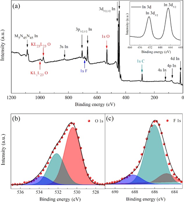
(a) XPS wide scan with an inset of In 3d core-level XPS spectra, (b) O 1s, and (c) F 1s core-level XPS spectra of the as-sputtered IFO:H film. The scatter plots in red color represent the experimental profiles, and the solid lines refer to the Gaussian components.
Figure 3b shows the O 1s XPS spectrum of the IFO:H film, which is fitted using three Gaussian components centered at 530.4, 532.2, and 533.7 eV. In2O3 crystallizes with a bixbyite structure in which each indium atom is surrounded by six oxygen atoms at the corners of a distorted cube, with two vacancies at the two unoccupied corners. According to the reported data,26 the lower energy peak located at 530.4 eV corresponds to O2– ions, which have neighboring In atoms with their full octahedral coordination environment, whereas the higher energy peak located at 532.2 eV is assigned to O2– ions in oxygen-deficient sites. Besides, the 533.7 eV peak is attributed to −OH groups, either from the film itself or from the air exposure, which will be further discussed by the FTIR approach. Figure 3c shows the F 1s XPS spectrum of the IFO:H film. It has been discussed that a fluorine atom substitutes an oxygen atom generating a free electron or occupies an oxygen vacancy site eliminating an electron trap site. Fluorine ions with strong electronegativity could form hydrogen bonds with hydroxyl groups, thus passivating the hole trap sites of the hydroxyl groups.26 The F 1s spectrum was fitted using three Gaussians at 684.8, 686.0, and 688.2 eV. Correspondingly, the component at 684.8 eV is related to fluorine of the In-F bond in the IFO film; the component at 686.0 eV is due to fluorine that occupies the oxygen vacancies; finally, the component at 688.2 eV is related to the F ions that form hydrogen bonds with surface hydroxyl groups.26,42
The composition results show that the atomic ratio of In/(O + F) is 0.69, similar to the reported values of In2O3 films.27 An oxygen deficiency of ∼3% has been observed with respect to the stoichiometric composition. Moreover, the F/(F + O) atomic ratio indicates 12% fluorine doping, and an F/In atomic ratio was calculated to be 17.4%. It has been reported that the F/In ratio has a significant influence on the contact properties between IFO and p-/n-type c-Si, regardless of the possible oxygen content variation.43 According to Untila et al.,43 the ratio of 17.4% is in a region that the IFO film forms an Ohmic contact with n-type c-Si, yet rectifying the contact with p-type c-Si. We have to note that the properties of TCOs are affected by various deposition technologies. The contact issues between our IFO film and the adjacent layers will be discussed in the following sections.
FTIR measurements were carried out to verify the existence of hydrogen. By comparison, a reference IFO sample with the same thickness without water vapor in the deposition was also measured. Figure 4a shows the FTIR spectra of the as-deposited samples. The bands at around 1600 and 3400 cm–1 could be attributed to bonded OH bending and stretching vibrations, respectively.44,45 The bands may come from either the films or physically adsorbed water,46 yet from a comparison between the sample with and without water vapor in the growth process (especially at 3400 cm–1), shift and intensity of the peaks changed significantly upon H2O vapor introduction, indicating strengthened hydrogen bonds and related redistribution in the IFO:H film.44 Thus, the existence of hydrogen could be proved. Besides, the observed bands in the 400–800 cm–1 region may be attributed to the characteristic M–O vibrations corresponding to In–O in the films.44,47 No fluorine-related band was observed.
Figure 4.

(a) FTIR spectra of the IFO:H and IFO films. (b) X-ray diffraction patterns for the optimized IFO:H film.
Furthermore, FTIR is also an informative method to estimate the conduction band electrons in n-type semiconductors. The absorbance exhibited by IFO:H in the mid-IR region (>1000 cm–1) has a positive correlation with the number of conduction band electrons in the film.48 The results clearly indicate that the water vapor in the deposition process can increase the conduction band electrons in the IFO:H film, and hence, improve the conductivity of the film. The results are in good agreement with the data reported in Figure 2, and the higher Ne could be attributed to the doped hydrogen acting as shallow donors.49,50 The above results indicate that the higher μe of the IFO:H film might be presumably attributed to contributions from the elimination of electron trap sites from fluorine doping26,51 and possible grain-boundary passivation by hydrogen,9,49 both of which lower the potential barriers, thus benefiting the carrier transport in the film.49,51
Figure 4b shows the XRD spectrum of the optimal IFO:H film. All peaks can be assigned to the cubic bixbyite structure of In2O3, which matches with ICDD database version PDF4+ reference code no. 04-004-8968, indicating that the IFO:H film retains the polycrystalline cubic In2O3 structure.52 The strongest (222) diffraction peak at 30.55° is conspicuous, other peaks were assigned accordingly.25,53 Besides, the broad background peak at around 2θ = 22.28° is related to the glass substrate.54 Furthermore, the mean crystallite size was calculated to be 29.85 nm from the full width at half-maximum (FWHM) of the X-ray peak of (222) following Scherrer’s formula.55
To understand the surface quality and growth morphology, the surface morphology and roughness of the IFO:H film were measured by an atomic force microscope (AFM), as shown in Figure 5. The film exhibits a rather smooth surface with a root-mean-square (RMS) roughness of 0.52 nm.
Figure 5.

(a) AFM micrograph of the optimal IFO:H film. (b) Cross-sectional profile along the line in (a).
3.3. Electrical and Optical Properties in Comparison with ITO
The electrical properties of the optimized IFO:H layer are listed in Table 1 and compared to those of the ITO reference. It was found that the introduction of fluorine causes an abrupt increase of μe in the fluorine-doped tin oxide (FTO) film, due to fluorine dopant lowering the transport barrier at the grain boundaries.56 In terms of physical definition, μe = eτ/ me*, where μe is the electron mobility and τ and me are carrier relaxation time and electron effective mass, respectively. It has been theoretically57 and experimentally11 found that high-μe TCO films exhibit a me* similar to those of conventional polycrystalline ITO and amorphous In2O3-based TCO films, indicating that high μe is mainly achieved through a larger τ rather than a smaller me.11 Therefore, as we mentioned above, the high μe in IFO:H might be interpreted by various scattering mechanisms (influencing τ) such as little distortion in the crystal structure,19 low barrier height at grain boundaries by fluorine doping,43 grain-boundary passivation by hydrogen, and the fact that hydrogen atoms in the film do not significantly contribute to ionized or neutral impurity scattering.9,49
Table 1. Electrical Parameters of the As-Deposited 75 nm Thick IFO:H and ITO Films.
| TCO | sheet resistance (Rsh, Ω/sq) | carrier density (Ne, cm–3) | electron mobility (μe, cm2 V–1 s–1) | resistivity (ρ, Ω cm) |
|---|---|---|---|---|
| IFO:H | 74 | 1.2 × 10²⁰ | 87 | 6.2 × 10⁻⁴ |
| ITO | 50 | 4.9 × 10²⁰ | 28 | 4.7 × 10⁻⁴ |
Figure 6a shows the transmittance and reflectance spectra of 75-nm-thick IFO:H and ITO films. Comparable transmittance was observed in the Vis-IR region, while in the UV range, the transmittance edge of the IFO:H film shows a blue shift relative to ITO, indicating a possible wider band gap in the IFO:H film. Furthermore, the IFO:H film displays higher reflectance in both UV and IR regions, which are related to the tail states and plasma oscillations of the free carriers, respectively.42,58Figure 6b illustrates the absorption coefficient (α) of the TCOs with an ASTM G173-03 solar spectrum provided in the background. The absorption coefficient was calculated from α = ln[(1 – R)2/T]/d, where T and R are the measured transmittance and reflectance spectra, respectively, and d is the film thickness. As can be seen, the IFO:H film shows lower α along the whole wavelength range, allowing an augmented light incidence to the absorber material of the PV devices. As previously mentioned, the absorption edge shifts toward the lower wavelength, indicating a wider band gap of the IFO:H film. The optical band gap (Eopt) for allowed direct electronic transition was calculated from the plot of (αhν)2 versus (hν) in Figure 6c.8 The IFO:H film has an Eopt of 3.85 eV, which is wider than that of ITO (3.76 eV). The wider band gap value should not be explained by the Moss–Burstein effect59 since the carrier density of the IFO:H film is lower than that of ITO. It has been proposed that the optical transitions in a specific material system are influenced by the disorder in the material phase,12 as well as the various interaction effects either between free carriers or between free carriers and ionized impurities.60
Figure 6.

Optical properties of the IFO:H and ITO films. (a) Transmittance and reflectance spectra, (b) calculated absorption coefficient curves, (c) optical band gap plot curves, and (d) the wavelength-dependent refractive index (n) and extinction coefficient (k) curves.
In low crystalline, disordered, and amorphous materials, an exponential tail called the Urbach tail appears near the optical band edge along the absorption coefficient curve. The Urbach tail is generated due to localized states in the band gap caused by perturbation in the structure and by a disorder of the system.58 We thus extracted the Urbach energy (EU) to estimate the width of the tail states, following the Urbach relation that ln α = ln α0 + (hν/EU), where α0 is a pre-exponential constant and (hν) is the incident photon.58 The fitting results showed an EU of 197 meV for the IFO:H film and 444 meV for ITO, respectively. Compared to ITO, higher Eopt and mobility can be expected from IFO:H due to its lower Urbach energy.58 Besides, the EU value of the IFO:H film is closer to the reported data of the high-mobility IO:H and IZO films (∼130 meV),8 indicating similar changes upon ITO, where the fluorine doping accompanies less disorder and defect states in the In2O3-based film. It is notable that the EU for ITO is higher than the reported value of 300 meV extracted from PDS measurements by Morales-Masis et al.,8 the reason may be attributed to the ITO material quality deposited by different sputtering technologies.
Furthermore, another particularly attractive feature of all In2O3-based materials is that their refractive index is close to 2 at around 600 nm wavelength, where solar radiation intensity is maximum. This is approximately the geometric mean of the refractive indices of air and typical solar cell absorber, such as silicon, and gives such materials very good antireflective coating (ARC) properties.9 The wavelength-dependent refractive index (n) and extinction coefficient (k) curves from Scout software fitting are shown in Figure 6d. n decreases with the wavelength, which is consistent with the expectation from Kramers–Kronig analysis.53 It is noticeable that the IFO:H has a relatively gentler variation in n than ITO, which may have a better ARC potential than the ITO film considering the wavelength-dependent phase changes in the light interference.61 Furthermore, k values are in accordance with the α curves in Figure 6b, which can be interpreted by the correlation of α = 4πk/λ, whereas the inconsistency between α and k in the UV region in the two figures should be attributed to the software fitting error in the region.
To summarize, compared to ITO, the IFO:H film has lower Ne, higher μe and n (especially in the IR range), which contributes to reducing FCA.62 Combined with the potential as ARC, the significant optical performance of the IFO:H film as a front electrode can be expected at the device level. Furthermore, considering the low absorption in the IR region, the IFO:H film deployed at the rear side of a PV device may also output an additional optical contribution.7
3.4. Application of the IFO:H Film as Electrode Contacts
We evaluated the WF values of the TCOs under test via the KPFM approach. Typical recorded CPD values were −895, −475, and −720 mV for gold (reference), IFO:H, and ITO films, respectively. Accordingly, the WF values were calculated to be 4.68 eV for IFO:H and 4.93 eV for ITO,34 indicating a preferable contact of IFO:H for collecting electrons from the n-contact stack in the solar cell device.63 The results may be interpreted with the reported model that fluorine reduces the oxygen content at the grain surface, and consequently decreases both the surface negative charge and the barrier height at the grain boundaries, resulting in a WF decrease in the case of the IFO:H film.43 The contact resistivity (ρc) between 75 nm thick TCOs and screen-printed silver (Ag) was studied using the transfer length method (TLM).35 Fitting results show that Ohmic contacts form between TCOs and Ag, which can be expected from the metal-like electronic behavior of the degenerated In2O3-based TCOs.64 The ρc values are 0.22 mΩ cm2 for the ITO/Ag stack and 1.13 mΩ cm2 for the IFO:H/Ag stack. The higher ρc in the IFO:H/Ag stack is related to the much lower carrier density (Ne) in the IFO:H film.9,10,64 This drawback might be circumvented by deploying a TCO bi-layer prior to metallization (e.g., transport layer/IFO:H/ITO/Ag).65
3.5. Solar Cells
In this section, we report the potential benefits of using IFO:H TCO in c-Si solar cells. Based on Figure 1b, three groups of solar cells with CSPCs were designed. Note that the IFO:H films were applied on the n-contact stack at the rear sides of poly-Si(Cx) hybrid solar cells, with a thickness of 150 nm to ensure a good infrared response,7 and on both sides of SHJ solar cells (75- and 150-nm-thick, respectively). Figure 7a–c shows the corresponding EQE results. For the poly-Si(Cx) hybrid devices, rear IFO:H contributes to the IR response, resulting from a higher R and in accordance with higher n in the IR range (as shown in Figure 6). In the case of SHJ solar cells, optical improvement along the whole wavelength range was detected for the IFO:H cell, with a Jsc_EQE increase of 1.53 mA cm–2 compared to the ITO-based cell. Notably, all these improvements in the long-wavelength range might make the IOF:H film a potentially competitive TCO for the bottom cell in perovskite/silicon tandem solar cells.66
Figure 7.

External quantum efficiency (EQE) curves of (a) poly-SiCx hybrid, (b) poly-Si hybrid, and (c) SHJ solar cells, respectively. Jsc_EQE were provided accordingly.
Figure 8a shows the FF comparison for the cells shown in Figure 7. Besides, IFO:H exhibits larger sheet resistance and resistivity than ITO (Table 1), and the contact resistivity of IFO:H/Ag is larger than that of ITO/Ag (Section 3.4). We observed that in different front metal coverage cases (12.5 and 6%), poly-Si(Cx) hybrid solar cells with rear IFO:H exhibited obviously more than 1%abs. FF improvements compared to the ITO counterpart. Considering the preferable contact of IFO:H for collecting electrons from the n-contact stack in the solar cell device, the observed experimentally higher FF with IFO:H could be reasonably attributed to its favorable WF match with the n-doped layers.63 As for SHJ cells, double-side IFO:H films result in a comparable FF with respect to ITO–ITO cell film arrangement. Furthermore, Figure 8b displays the i-Voc change caused by TCO deposition. Compared with the initial cell precursors, the loss of i-Voc are found to be less than 5 mV, for both sputtered ITO and IFO:H films. This may provide a favorable approach for solar cells with CSPCs, especially for FBC solar cell architectures solely based on poly-Si CSPCs,67 whose surface passivation quality can experience severe loss upon TCO sputtering and might not be completely recovered with low post-annealing temperature.6,68 Besides, it is worth noting that the IFO:H film presents excellent optoelectronic properties already from the as-deposited step, displaying an advantage over ITO. Considering also that the deposition is performed at substrate temperatures below 110 °C and at low power densities, the IFO:H film may present ideal properties for application in some other temperature- and damage-sensitive technologies, such as polymer and perovskite solar cells, perovskite/silicon tandem solar cells, as well as flexible and paper electronics.8 Additionally, upon further optimization of cell design, with a front metal coverage of 4.4%, the 3.92 cm2 device performances based on three SHJ cells are shown in Table 2. Notably, the best SHJ solar cell with double-side IFO:H films illustrated an efficiency of 21.1%, whose current–voltage characteristic is presented in Figure 8c, and the best reference ITO-based SHJ solar cell showed an efficiency of 20.3%, with Voc = 702 mV, Jsc = 37.00 mA cm–2, and FF = 78.00%.
Figure 8.

(a) Fill factor (FF) of different types of solar cells with IFO:H applied on the n-contact stack at the rear sides of poly-Si(Cx) hybrid, and on both sides of SHJ solar cells, compared to ITO-based devices as references. Results from different metal coverages are provided. (b) Implied Voc variation with TCOs’ sputtering processes based on four series of experimental data, and (c) current–voltage characteristics of the best SHJ solar cells integrating double-side IFO:H films.
Table 2. Solar Cell Parameters of 3.92 cm2 SHJ Devices with IFO:H and ITOa.
| open-circuit voltage (Voc, mV) | short-circuit current density (Jsc, mA cm–2) | fill factor (FF, %) | efficiency (η, %) | |
|---|---|---|---|---|
| IFO:H | 702 ± 2.7 | 38.32 ± 0.17 | 78.08 ± 0.36 | 21.01 ± 0.08 |
| ITO | 699 ± 3.0 | 36.90 ± 0.10 | 78.18 ± 0.18 | 20.17 ± 0.12 |
The values reported are the average based on three cells. The standard deviation is calculated for each cell parameter.
4. Conclusions
We demonstrate RF-sputtered hydrogenated fluorine-doped indium oxide (IFO:H) films at low substrate temperature (<110 °C) and power density (<2.0 W cm–2). By varying the water vapor pressure during the deposition, we obtain an optimized IFO:H film with a remarkably high electron mobility (μe = 87 cm2 V–1 s–1), the optimal IFO:H film shows a cubic In2O3 polycrystalline structure with a F/In atomic ratio of 17.4%. Compared to ITO, the IFO:H film displays a wider optical band gap (3.85 eV), lower Urbach energy (197 meV), higher μe, and an appropriate refractive index for ARC purpose in Si-based devices. The high μe in IFO:H might be related to little distortion in the crystal structure, lower barrier height at grain boundaries by fluorine doping, and grain-boundary passivation by hydrogen. Using the IFO:H film on the rear sides of poly-Si(Cx) hybrid solar cells, we observed enhanced infrared spectral response and more than 1%abs. improvement in the FF mainly due to a favorable work function match between IFO:H and n-type doped layers, while the SHJ device with double-side IFO:H exhibited a Jsc_EQE gain of 1.53 mA cm–2 within the whole wavelength range without any FF loss. The optimized SHJ solar cell showed a conversion efficiency of 21.1%, featuring a Jsc of 38.49 mA cm–2, a Voc of 705 mV, and an FF of 77.72%. The IFO:H film could be a versatile candidate for applications such as poly-Si(Cx)(Ox)/SiO2, perovskite, perovskite/silicon tandem solar cells, and (flexible) optoelectronic devices.
Acknowledgments
The authors thank Else Kooi Laboratory at TU Delft for the experimental support, as well as Stefaan Heirman, Rudi Santbergen, Andres Calcabrini, Yilei Tian, and Daniele Sciré for the characterization setups and software analysis in various measurements. The work has been partly financially supported by the Shenzhen Institute of Wide-band gap Semiconductors. C.H. and X.Zh. gratefully acknowledge the support from the National Key Research and Development Program of China (Grant No. 2018YFB1500103), the National Natural Science Foundation of China (Grant No. 61674084), the Overseas Expertise Introduction Project for Discipline Innovation of Higher Education of China (Grant No. B16027), Tianjin Science and Technology Project (Grant No. 18ZXJMTG00220).
Author Contributions
This manuscript was written through contributions of all authors. All authors have given approval to the final version of the manuscript.
The authors declare no competing financial interest.
References
- Melskens J.; van de Loo B. W. H.; Macco B.; Black L. E.; Smit S.; Kessels W. M. M. Passivating Contacts for Crystalline Silicon Solar Cells: From Concepts and Materials to Prospects. IEEE J. Photovoltaics 2018, 8, 373–388. 10.1109/JPHOTOV.2018.2797106. [DOI] [Google Scholar]
- Taguchi M.; Yano A.; Tohoda S.; Matsuyama K.; Nakamura Y.; Nishiwaki T.; Fujita K.; Maruyama E. 24.7% Record Efficiency HIT Solar Cell on Thin Silicon Wafer. IEEE J. Photovoltaics 2014, 4, 96–99. 10.1109/JPHOTOV.2013.2282737. [DOI] [Google Scholar]
- Yoshikawa K.; Yoshida W.; Irie T.; Kawasaki H.; Konishi K.; Ishibashi H.; Asatani T.; Adachi D.; Kanematsu M.; Uzu H.; Yamamoto K. Exceeding Conversion Efficiency of 26% by Heterojunction Interdigitated Back Contact Solar Cell with Thin Film Si Technology. Sol. Energy Mater. Sol. Cells 2017, 173, 37–42. 10.1016/j.solmat.2017.06.024. [DOI] [Google Scholar]
- Richter A.; Benick J.; Feldmann F.; Fell A.; Hermle M.; Glunz S. W. n-Type Si Solar Cells with Passivating Electron Contact: Identifying Sources for Efficiency Limitations by Wafer Thickness and Resistivity Variation. Sol. Energy Mater. Sol. Cells 2017, 173, 96–105. 10.1016/j.solmat.2017.05.042. [DOI] [Google Scholar]
- Haase F.; Hollemann C.; Schäfer S.; Merkle A.; Rienäcker M.; Krügener J.; Brendel R.; Peibst R. Laser Contact Openings for Local Poly-Si-Metal Contacts Enabling 26.1%-efficient POLO-IBC Solar Cells. Sol. Energy Mater. Sol. Cells 2018, 186, 184–193. 10.1016/j.solmat.2018.06.020. [DOI] [Google Scholar]
- Feldmann F.; Ritzau K.-U.; Bivour M.; Moldovan A.; Modi S.; Temmler J.; Hermle M.; Glunz S. W. High and Low Work Function Materials for Passivated Contacts. Energy Procedia 2015, 77, 263–270. 10.1016/j.egypro.2015.07.037. [DOI] [Google Scholar]
- Holman Z. C.; Filipič M.; Descoeudres A.; De Wolf S.; Smole F.; Topič M.; Ballif C. Infrared Light Management in High-Efficiency Silicon Heterojunction and Rear-Passivated Solar Cells. J. Appl. Phys. 2013, 113, 013107 10.1063/1.4772975. [DOI] [Google Scholar]
- Morales-Masis M.; Nicolas S. M. D.; Holovsky J.; Wolf S. D.; Ballif C. Low-Temperature High-Mobility Amorphous IZO for Silicon Heterojunction Solar Cells. IEEE J. Photovoltaics 2015, 5, 1340–1347. 10.1109/JPHOTOV.2015.2450993. [DOI] [Google Scholar]
- Morales-Masis M.; De Wolf S.; Woods-Robinson R.; Ager J. W.; Ballif C. Transparent Electrodes for Efficient Optoelectronics. Adv. Electron. Mater. 2017, 3, 1600529 10.1002/aelm.201600529. [DOI] [Google Scholar]
- Procel P.; Haiyuan X.; Senaud L. L.; Paviet-Salomon B.; Radhakrishnan H. S.; Filipič M.; Menglei X.; Boccard M.; Fioretti A.; Monnard R.; Stang J. C.; Wagner P.; Meza D.; Lachenal D.; Strahm B.; Duang W.; Lambertz A.; Fejfar A.; Ding K.; Despeisse M.; Gordon I.; Korte L.; Ballif C.; Isabella O.; Zeman M. In On the correlation between resistivity and high efficiency (IBC-)SHJ solar cells. Proceedings of the 36th European Photovoltaic Solar Energy Conference and Exhibition, 2019; pp 255−258.
- Koida T.; Ueno Y.; Shibata H. In2O3-Based Transparent Conducting Oxide Films with High Electron Mobility Fabricated at Low Process Temperatures. Phys. Status Solidi A 2018, 215, 1700506 10.1002/pssa.201700506. [DOI] [Google Scholar]
- Wardenga H.; Frischbier V. M.; Morales-Masis M.; Klein A. In Situ Hall Effect Monitoring of Vacuum Annealing of In2O3:H Thin Films. Materials 2015, 8, 561–574. 10.3390/ma8020561. [DOI] [PMC free article] [PubMed] [Google Scholar]
- Kobayashi E.; Watabe Y.; Yamamoto T.; Yamada Y. Cerium Oxide and Hydrogen Co-Doped Indium Oxide Films for High-Efficiency Silicon Heterojunction Solar Cells. Sol. Energy Mater. Sol. Cells 2016, 149, 75–80. 10.1016/j.solmat.2016.01.005. [DOI] [Google Scholar]
- van Hest M. F. A. M.; Dabney M. S.; Perkins J. D.; Ginley D. S.; Taylor M. P. Titanium-Doped Indium Oxide: A High-Mobility Transparent Conductor. Appl. Phys. Lett. 2005, 87, 032111 10.1063/1.1995957. [DOI] [Google Scholar]
- Morales-Masis M.; Rucavado E.; Monnard R.; Barraud L.; Holovský J.; Despeisse M.; Boccard M.; Ballif C. Highly Conductive and Broadband Transparent Zr-Doped In2O3 as Front Electrode for Solar Cells. IEEE J. Photovoltaics 2018, 8, 1202–1207. 10.1109/JPHOTOV.2018.2851306. [DOI] [Google Scholar]
- Meng F.; Shi J.; Liu Z.; Cui Y.; Lu Z.; Feng Z. High Mobility Transparent Conductive W-Doped In2O3 Thin Films Prepared at Low Substrate Temperature and its Application to Solar Cells. Sol. Energy Mater. Sol. Cells 2014, 122, 70–74. 10.1016/j.solmat.2013.11.030. [DOI] [Google Scholar]
- Meng Y.; Yang X.; Chen H.; Shen J.; Jiang Y.; Zhang Z.; Hua Z. Molybdenum-Doped Indium Oxide Transparent Conductive Thin Films. J. Vac. Sci. Technol., A 2002, 20, 288–290. 10.1116/1.1421595. [DOI] [Google Scholar]
- Wang G. H.; Shi C. Y.; Zhao L.; Diao H. W.; Wang W. J. Transparent Conductive Hf-Doped In2O3 Thin Films by RF Sputtering Technique at Low Temperature Annealing. Appl. Surf. Sci. 2017, 399, 716–720. 10.1016/j.apsusc.2016.11.239. [DOI] [Google Scholar]
- Singh S.; Raza A.; Sharma A.; Agnihotri O.; Tewari L. Characterization of Fluorine-Doped In2O3 Films Synthesized by Spray Pyrolysis. Thin Solid Films 1983, 105, 131–138. 10.1016/0040-6090(83)90201-8. [DOI] [Google Scholar]
- Maruyama T.; Nakai T. Fluorine-Doped Indium Oxide Thin Films Prepared by Chemical Vapor Deposition. J. Appl. Phys. 1992, 71, 2915–2917. 10.1063/1.351023. [DOI] [Google Scholar]
- Untila G. G.; Kost T. N.; Chebotareva A. B.; Zaks M. B.; Sitnikov A. M.; Solodukha O. I. Effect of Conditions of Deposition and Annealing of Indium Oxide Films Doped with Fluorine (IFO) on the Photovoltaic Properties of the IFO/p-Si Heterojunction. Semiconductors 2008, 42, 406. 10.1134/S1063782608040076. [DOI] [Google Scholar]
- Kobayashi H.; Ishida T.; Nakamura K.; Nakato Y.; Tsubomura H. Properties of Indium Tin Oxide Films Prepared by the Electron Beam Evaporation Method in Relation to Characteristics of Indium Tin Oxide/Silicon Oxide/Silicon Junction Solar Cells. J. Appl. Phys. 1992, 72, 5288–5293. 10.1063/1.352013. [DOI] [Google Scholar]
- Ishida T.; Kobayashi H.; Nakato Y. Structures and Properties of Electron-Beam-Evaporated Indium Tin Oxide Films as Studied by X-Ray Photoelectron Spectroscopy and Work-Function Measurements. J. Appl. Phys. 1993, 73, 4344–4350. 10.1063/1.352818. [DOI] [Google Scholar]
- Avaritsiotis J. N.; Howson R. P. Composition and Conductivity of Fluorine-Doped Conducting Indium Oxide Films Prepared by Reactive Ion Plating. Thin Solid Films 1981, 77, 351–357. 10.1016/0040-6090(81)90329-1. [DOI] [Google Scholar]
- Shigesato Y.; Shin N.; Kamei M.; Song P. K.; Yasui I. Study on Fluorine-Doped Indium Oxide Films Deposited by RF Magnetron Sputtering. Jpn. J. Appl. Phys. 2000, 39, 6422–6426. 10.1143/JJAP.39.6422. [DOI] [Google Scholar]
- Seo J.-S.; Jeon J.-H.; Hwang Y. H.; Park H.; Ryu M.; Park S.-H. K.; Bae B.-S. Solution-Processed Flexible Fluorine-Doped Indium Zinc Oxide Thin-Film Transistors Fabricated on Plastic Film at Low Temperature. Sci. Rep. 2013, 3, 2085 10.1038/srep02085. [DOI] [PMC free article] [PubMed] [Google Scholar]
- Mayer B. Highly Conductive and Transparent Films of Tin and Fluorine Doped Indium Oxide Produced by APCVD. Thin Solid Films 1992, 221, 166–182. 10.1016/0040-6090(92)90811-O. [DOI] [Google Scholar]
- Untila G. G.; Kost T. N.; Chebotareva A. B.; Kireeva E. D. Contact Resistance of Indium Tin Oxide and Fluorine-Doped Indium Oxide Films Grown by Ultrasonic Spray Pyrolysis to Diffusion Layers in Silicon Solar Cells. Sol. Energy Mater. Sol. Cells 2015, 137, 26–33. 10.1016/j.solmat.2015.01.018. [DOI] [Google Scholar]
- Untila G. G.; Kost T. N.; Chebotareva A. B. Concentrator In2O3:F/(n+pp+)c-Si/Al Solar Cells with Al-alloyed BSF and Ag-free Multi-Wire Metallization Using Transparent Conductive Polymers. Sol. Energy 2018, 174, 1008–1015. 10.1016/j.solener.2018.09.076. [DOI] [Google Scholar]
- Holman Z. C.; Descoeudres A.; Barraud L.; Fernandez F. Z.; Seif J. P.; Wolf S. D.; Ballif C. Current Losses at the Front of Silicon Heterojunction Solar Cells. IEEE J. Photovoltaics 2012, 2, 7–15. 10.1109/JPHOTOV.2011.2174967. [DOI] [Google Scholar]
- Sap J. A.; Isabella O.; Jäger K.; Zeman M. Extraction of Optical Properties of Flat and Surface-Textured Transparent Conductive Oxide Films in a Broad Wavelength Range. Thin Solid Films 2011, 520, 1096–1101. 10.1016/j.tsf.2011.08.023. [DOI] [Google Scholar]
- Matthew J. Surface Analysis by Auger and X-Ray Photoelectron Spectroscopy. D. Briggs and J. T. Grant (eds). IMPublications: Chichester, UK and SurfaceSpectra, Manchester, UK, 2003. 900 pp., ISBN 1-901019-04-7, 900 pp. Surf. Interface Anal. 2004, 36, 1647. 10.1002/sia.2005. [DOI] [Google Scholar]
- Gulino A. Structural and Electronic Characterization of Self-Assembled Molecular Nanoarchitectures by X-Ray Photoelectron Spectroscopy. Anal. Bioanal. Chem. 2013, 405, 1479–1495. 10.1007/s00216-012-6394-8. [DOI] [PubMed] [Google Scholar]
- Salerno M.; Dante S. Scanning Kelvin Probe Microscopy: Challenges and Perspectives towards Increased Application on Biomaterials and Biological Samples. Materials 2018, 11, 951. 10.3390/ma11060951. [DOI] [PMC free article] [PubMed] [Google Scholar]
- Schube J.; Tutsch L.; Fellmeth T.; Bivour M.; Feldmann F.; Hatt T.; Maier F.; Keding R.; Clement F.; Glunz S. W. Low-Resistivity Screen-Printed Contacts on Indium Tin Oxide Layers for Silicon Solar Cells With Passivating Contacts. IEEE J. Photovoltaics 2018, 8, 1208–1214. 10.1109/JPHOTOV.2018.2859768. [DOI] [Google Scholar]
- Limodio G.; Yang G.; Ge H.; Procel P.; De Groot Y.; Mazzarella L.; Isabella O.; Zeman M. Front and Rear Contact Si Solar Cells Combining High and Low Thermal Budget Si Passivating Contacts. Sol. Energy Mater. Sol. Cells 2019, 194, 28–35. 10.1016/j.solmat.2019.01.039. [DOI] [Google Scholar]
- Nogay G.et al. Full-Area Passivating Contacts with High and Low Thermal Budgets: Solutions for High Efficiency c-Si Solar Cells. EPFL Thesis; EPFL: Lausanne, 2018. [Google Scholar]
- Yang G.; Guo P.; Procel P.; Limodio G.; Weeber A.; Isabella O.; Zeman M. High-Efficiency Black IBC c-Si Solar Cells with Poly-Si as Carrier-Selective Passivating Contacts. Sol. Energy Mater. Sol. Cells 2018, 186, 9–13. 10.1016/j.solmat.2018.06.019. [DOI] [Google Scholar]
- Honda S.; Watamori M.; Oura K. The Effects of Oxygen Content on Electrical and Optical Properties of Indium Tin Oxide Films Fabricated by Reactive Sputtering. Thin Solid Films 1996, 281–282, 206–208. 10.1016/0040-6090(96)08614-2. [DOI] [Google Scholar]
- Shen L.; An Y.; Cao D.; Wu Z.; Liu J. Room-Temperature Ferromagnetic Enhancement and Crossover of Negative to Positive Magnetoresistance in N-Doped In2O3 Films. J. Phys. Chem. C 2017, 121, 26499–26506. 10.1021/acs.jpcc.7b08732. [DOI] [Google Scholar]
- Kato H.; Takemura S.; Nakajima Y. X-Ray Photoemission Spectroscopy Studies of Conducting Polymer-Substrate Interfaces: Interfacial Electrochemical Diffusion. J. Appl. Phys. 1997, 81, 7313–7316. 10.1063/1.365353. [DOI] [Google Scholar]
- Singh S. P.; Tiwari L. M.; Agnihotri O. P. Optical Investigations of In2O3: F Films. Thin Solid Films 1986, 139, 1–7. 10.1016/0040-6090(86)90041-6. [DOI] [Google Scholar]
- Untila G. G.; Kost T. N.; Chebotareva A. B. Fluorine Doped Indium Oxide Films for Silicon Solar Cells. Thin Solid Films 2009, 518, 1345–1349. 10.1016/j.tsf.2009.02.152. [DOI] [Google Scholar]
- Sugumaran S.; Bellan C. S.; Muthu D.; Raja S.; Bheeman D.; Rajamani R. Novel Hybrid PVA–InZnO Transparent Thin Films and Sandwich Capacitor Structure by Dip Coating Method: Preparation And Characterizations. RSC Adv. 2015, 5, 10599–10610. 10.1039/C4RA14817G. [DOI] [Google Scholar]
- Myilsamy M.; Murugesan V.; Mahalakshmi M. Indium and Cerium Co-Doped Mesoporous TiO2 Nanocomposites with Enhanced Visible Light Photocatalytic Activity. Appl. Catal., A 2015, 492, 212–222. 10.1016/j.apcata.2014.12.035. [DOI] [Google Scholar]
- Sugumaran S.; Bellan C. S.; Muthu D.; Raja S.; Bheeman D.; Rajamani R. New Transparent PVA-InTiO Hybrid Thin Films: Influence of InTiO on the Structure, Morphology, Optical, and Dielectric Properties. Polym. Adv. Technol. 2015, 26, 1486–1493. 10.1002/pat.3568. [DOI] [Google Scholar]
- Pashchanka M.; Hoffmann R. C.; Gurlo A.; Schneider J. J. Molecular Based, Chimie Douce Approach to 0D and 1D Indium Oxide Nanostructures. Evaluation of their Sensing Properties towards CO and H2. J. Mater. Chem. 2010, 20, 8311–8319. 10.1039/c0jm01490g. [DOI] [Google Scholar]
- Siedl N.; Gügel P.; Diwald O. First Combined Electron Paramagnetic Resonance and FT-IR Spectroscopic Evidence for Reversible O2 Adsorption on In2O3–x Nanoparticles. J. Phys. Chem. C 2013, 117, 20722–20729. 10.1021/jp4069834. [DOI] [Google Scholar]
- Macco B.; Knoops H. C. M.; Kessels W. M. M. Electron Scattering and Doping Mechanisms in Solid-Phase-Crystallized In2O3:H Prepared by Atomic Layer Deposition. ACS Appl. Mater. Interfaces 2015, 7, 16723–16729. 10.1021/acsami.5b04420. [DOI] [PubMed] [Google Scholar]
- Limpijumnong S.; Reunchan P.; Janotti A.; Van de Walle C. G. Hydrogen Doping in Indium Oxide: An ab Initio Study. Phys. Rev. B 2009, 80, 193202 10.1103/PhysRevB.80.193202. [DOI] [Google Scholar]
- Ellmer K.; Klein A.; Rech B., Transparent Conductive Zinc Oxide: Basics and Applications in Thin Film Solar Cells; Springer Science & Business Media, 2007; Vol. 104, pp 59–61. [Google Scholar]
- Yu Z. G.; Sun J.; Sullivan M. B.; Zhang Y.-W.; Gong H.; Singh D. J. Dopant Chemical Potential Modulation on Oxygen Vacancies Formation in In2O3: A Comparative Density Functional Study. Chem. Phys. Lett. 2015, 621, 141–145. 10.1016/j.cplett.2015.01.008. [DOI] [Google Scholar]
- Wu W.-F.; Chiou B.-S.; Hsieh S.-T. Effect of Sputtering Power on the Structural and Optical Properties of RF Magnetron Sputtered ITO Films. Semicond. Sci. Technol. 1994, 9, 1242. 10.1088/0268-1242/9/6/014. [DOI] [Google Scholar]
- Amara S.; Bouafia M. Characterisation of TCO AZO/Glass Structures by Spectroscopic Ellipsometry. Int. J. Nanopart. 2013, 6, 122. 10.1504/IJNP.2013.054987. [DOI] [Google Scholar]
- Parsianpour E.; Raoufi D.; Roostaei M.; Sohrabi B.; Samavat F. Characterization and Structural Property of Indium Tin Oxide Thin Films. Adv. Mater. Phys. Chem. 2017, 07, 42–57. 10.4236/ampc.2017.72005. [DOI] [Google Scholar]
- Shanthi E.; Banerjee A.; Dutta V.; Chopra K. L. Electrical and Optical Properties of Tin Oxide Films Doped with F and (Sb+F). J. Appl. Phys. 1982, 53, 1615–1621. 10.1063/1.330619. [DOI] [Google Scholar]
- Medvedeva J. E. Combining Optical Transparency with Electrical Conductivity: Challenges and Prospects. Transparent Electron. 2010, 1–29. 10.1002/9780470710609.ch1. [DOI] [Google Scholar]
- Hassanien A. S.; Akl A. A. Effect of Se Addition on Optical and Electrical Properties of Chalcogenide CdSSe Thin Films. Superlattices Microstruct. 2016, 89, 153–169. 10.1016/j.spmi.2015.10.044. [DOI] [Google Scholar]
- Köstlin H.; Jost R.; Lems W. Optical and Electrical Properties of Doped In2O3 Films. Phys. Status Solidi A 1975, 29, 87–93. 10.1002/pssa.2210290110. [DOI] [Google Scholar]
- Thirumoorthi M.; Thomas Joseph Prakash J. Structure, Optical and Electrical Properties of Indium Tin Oxide Ultra Thin Films Prepared by Jet Nebulizer Spray Pyrolysis Technique. J. Asian Ceram. Soc. 2016, 4, 124–132. 10.1016/j.jascer.2016.01.001. [DOI] [Google Scholar]
- Hossain M. I.; Qarony W.; Jovanov V.; Tsang Y. H.; Knipp D. Nanophotonic Design of Perovskite/Silicon Tandem Solar Cells. J. Mater. Chem. A 2018, 6, 3625–3633. 10.1039/C8TA00628H. [DOI] [Google Scholar]
- Liu C. P.; Foo Y.; Kamruzzaman M.; Ho C. Y.; Zapien J. A.; Zhu W.; Li Y. J.; Walukiewicz W.; Yu K. M. Effects of Free Carriers on the Optical Properties of Doped CdO for Full-Spectrum Photovoltaics. Phys. Rev. Appl. 2016, 6, 064018 10.1103/PhysRevApplied.6.064018. [DOI] [Google Scholar]
- Procel P.; Yang G.; Isabella O.; Zeman M. Theoretical Evaluation of Contact Stack for High Efficiency IBC-SHJ Solar Cells. Sol. Energy Mater. Sol. Cells 2018, 186, 66–77. 10.1016/j.solmat.2018.06.021. [DOI] [Google Scholar]
- Nghiem G. M.; Kristiansen H.; Aasmundtveit K. In Investigation of Contacts between Metal and Transparent Conductive Oxides, 2016 6th Electronic System-Integration Technology Conference (ESTC), 13-15 Sept. 2016, 2016; pp 1–4.
- Barraud L.; Holman Z. C.; Badel N.; Reiss P.; Descoeudres A.; Battaglia C.; De Wolf S.; Ballif C. Hydrogen-Doped Indium Oxide/Indium Tin Oxide Bilayers for High-Efficiency Silicon Heterojunction Solar Cells. Sol. Energy Mater. Sol. Cells 2013, 115, 151–156. 10.1016/j.solmat.2013.03.024. [DOI] [Google Scholar]
- Leilaeioun M.; Yu Z. J.; Holman Z. In Optimization of Front TCO Layer of Silicon Heterojunction Solar Cells for Tandem Applications, 2016 IEEE 43rd Photovoltaic Specialists Conference (PVSC), 5-10 June 2016, 2016; pp 0681–0684.
- Yang G.; Guo P.; Procel P.; Weeber A.; Isabella O.; Zeman M. Poly-Crystalline Silicon-Oxide Films as Carrier-Selective Passivating Contacts for c-Si Solar Cells. Appl. Phys. Lett. 2018, 112, 193904 10.1063/1.5027547. [DOI] [Google Scholar]
- Tutsch L.; Feldmann F.; Polzin J.; Luderer C.; Bivour M.; Moldovan A.; Rentsch J.; Hermle M. Implementing transparent conducting oxides by DC sputtering on ultrathin SiOx / poly-Si passivating contacts. Sol. Energy Mater. Sol. Cells 2019, 200, 109960 10.1016/j.solmat.2019.109960. [DOI] [Google Scholar]