Abstract

Dual-gate thin-film transistors (DGTFTs) have attracted increasing attention in the past few years because of threshold voltage modulation and device logic functionality. Here, solution-processed chitosan-based proton conductors are used as the gate dielectric. The threshold voltage shift depends on the ratio of the capacitances of the two gate dielectrics. The second interesting application of DGTFTs is logic functionality. This device demonstrates AND logic function controlled by applying either 0 or −1 V to each of the gate electrodes. When both gates were simultaneously applied to be 0 V, the current flows (ON). Otherwise, the current is blocked (OFF). In order to provide a comprehensive overview of these paper devices, the planarization of paper surface and switching stability of such DGTFTs are all discussed.
1. Introduction
In 1981, one of the first dual-gate thin-film transistors (DGTFTs) based on CdSe was reported by Luo et al.1 From then on, many kinds of DGTFTs were reported.2−5 The advantages of DGTFTs reported by many researchers are steeper subthreshold slope and increased gate modulation. The second gate electrostatically modifies the charge carrier distribution in the channel accumulated by the first gate, so the second gate can set threshold voltage (Vth) accurately.2 The threshold voltage can be set as a function of the applied biases, and the effective threshold voltage shift depends on the ratio of the capacitances of the two gate dielectrics. Besides setting the threshold voltage to modulate the operation mode of DGTFTs, such devices are demonstrated as AND gates. Several circuit applications of utilizing DGTFTs have already been reported;2,6 however, it does not make full use of the special advantages of DGTFTs. Numerous logic circuits which are widely used in devices require multiple inputs, while this functionality can be achieved by using a single DGTFT. Hence, the number of transistors required in many digital applications is reduced and the circuits are simplified. These advantages can be used to realize new functional devices.
Recently, a new kind of transistor, called junctionless transistor, has been reported.7−9 In this paper, all the channel and source/drain electrodes of such junctionless DGTFTs are realized by a thin indium tin oxide (ITO) film without any source/drain junction formation. Such a junctionless paper transistor shows high promise for future electronics application because of simple device process and low-cost paper substrates. Paper is an intriguing alternative to fulfill low-cost demand because it is ubiquitous in daily life and the cheapest flexible substrate. Moreover, paper is also environmentally friendly because it is recyclable and made of renewable raw materials.10 However, the paper surface is rough and porous; until now, it is still a challenging test to fabricate TFTs on the paper substrate. To solve this problem, the SiO2 film is used as a buffer layer to realize planarization of paper surface, which has been discussed in our previous paper.11 TFTs on paper substrates with higher than 10 V operation voltage have been reported by several groups;12,13 however, the device performance and stability are still far from satisfaction to be used for portable applications. Thus, to fabricate a low-voltage paper TFT, novel gate dielectric materials that offer both high gate-specific capacitance and low-temperature processability are in high demand. Recently, polymer electrolytes14 and inorganic nanogranular electrolytes15 with huge electric double layer (EDL) capacitances have been reported. In this paper, solution-processed chitosan films with huge EDL gate-specific capacitance are used as the gate dielectric layers. The major advantage of the EDL effect in chitosan dielectric is that the specific capacitance is extremely large at low frequencies, so that a small gate voltage variation (∼1.5 V) could induce several orders of magnitudes’ change in the drain current.
2. Results and Discussion
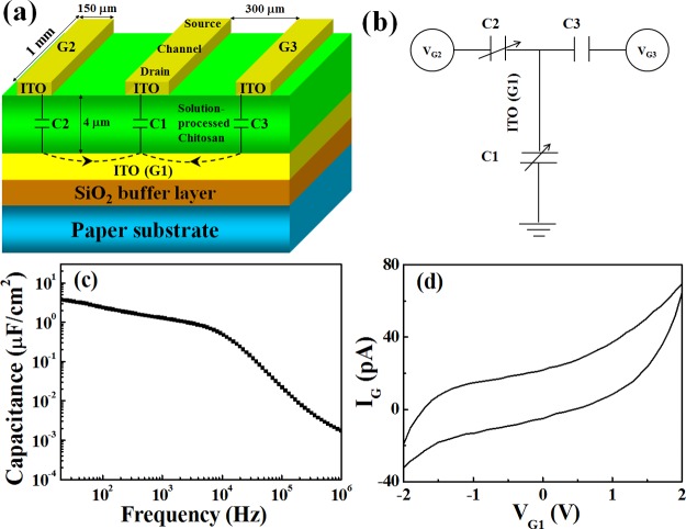
The schematic diagram of the proposed junctionless dual in-plane-gate paper TFTs is shown in Figure 1a. The capacitance of DGTFTs can be coupled by the bottom ITO layer has been reported by our previous work.16 As shown in Figure 1b, three capacitors (C1, C2, and C3) are coupled by the bottom ITO layer (G1), and the operation mechanism of such DGTFTs is demonstrated by the equivalent circuit. Thus, the channel current IDS controlled by one gate electrode (G2) can be modulated by the other gate electrode (G3). In order to understand the operation mechanism of the junctionless dual in-plane-gate paper TFTs, the specific capacitance of chitosan dielectric is measured. As shown in Figure 1c, when decreasing frequency, the capacitance of chitosan dielectric increases and reaches to 3.7 μF/cm2 at 20 Hz. The gate leakage current is shown in Figure 1d, and an ultralow leakage current (<80 pA) was observed.
Figure 1.
(a) Schematic picture of junctionless dual-gate paper TFTs. (b) Equivalent circuit of such junctionless DGTFTs. (c) Specific gate capacitance of junctionless dual-gate paper TFTs. (d) Leakage current of such TFTs.
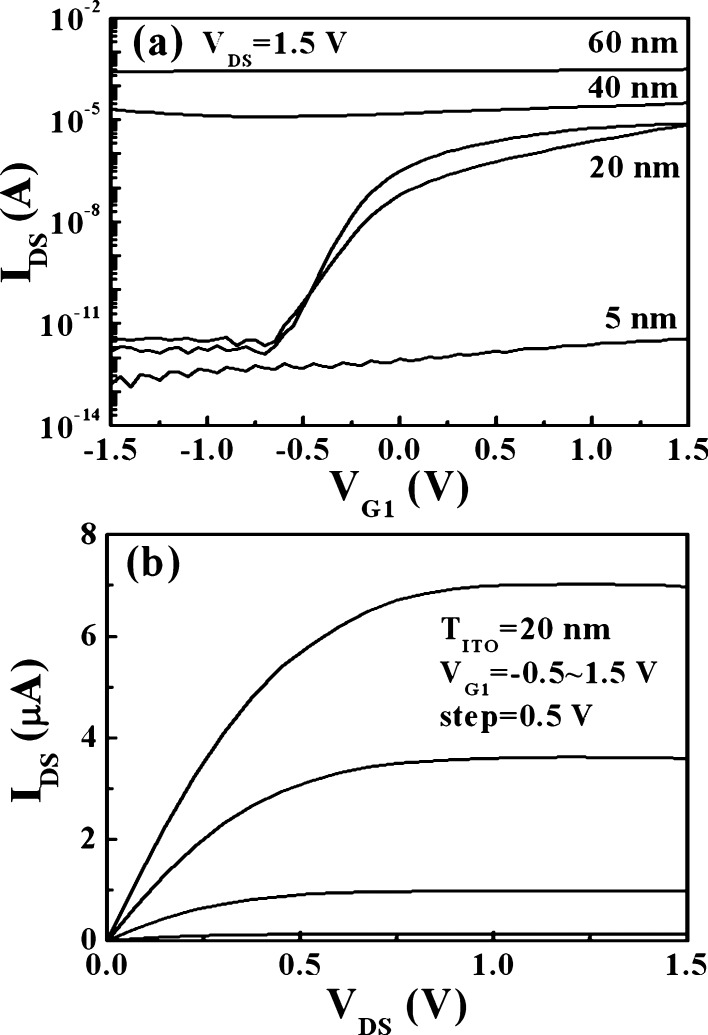
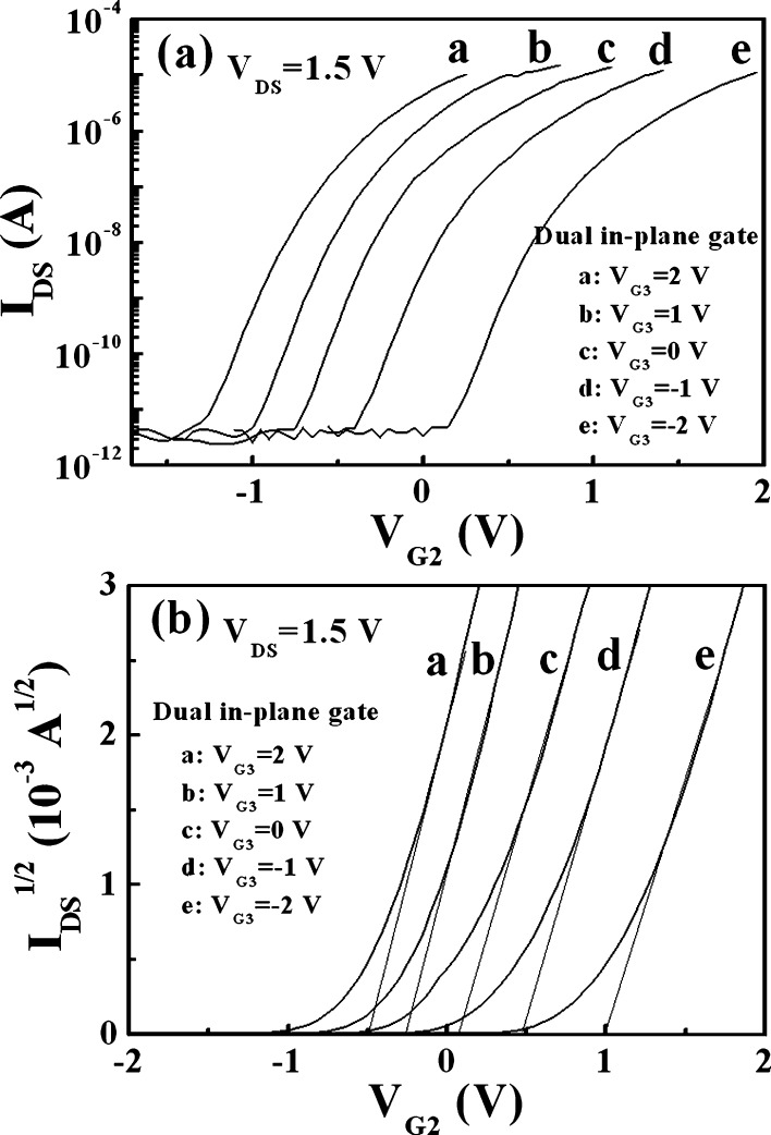
Figure 2a shows the transfer curves of such junctionless DGTFTs with different channel thicknesses (TITO = 5, 20, 40, and 60 nm) at a fixed VDS = 1.5 V. The bottom gate (G1) has no modulation effect on the channel current (IDS) when TITO = 5, 40, and 60 nm. However, the bottom gate shows effective modulation effect on the channel current when TITO = 20 nm. The subthreshold swing (S) and current on/off ratio (Ion/off) were calculated to be 0.12 V/dec and 5.8 × 10⁶, respectively. The channel length is 1 mm, the channel width is 0.15 mm, the specific capacitance of chitosan dielectric is 3.7 μF/cm2, IDS = 7 μA at VG1 = 1.5 V and Vth = 0.1 V, according to the equation of IDS = (WCiμ/2L)(VG1 – Vth)2, and the field-effect mobility (μsat) is calculated to be 12.8 cm2/Vs. Figure 2b shows the output curves of such junctionless DGTFTs with 20 nm channel thickness, and the bottom gate voltage increased from −0.5 to 1.5 V. It reveals excellent linear characteristics at low drain/source voltage and good current saturation behaviors at high drain/source voltage. The transfer characteristics with a constant VDS of 1.5 V of such junctionless DGTFTs is shown in Figure 3a, which shows that the transfer curves would shift from negative direction to positive direction when the secondary gate voltage decreased from 2.0 to −2.0 V.
Figure 2.
(a) IDS–VGS curves of junctionless DGTFTs on paper substrates with various channel thicknesses (TITO = 5, 20, 40, and 60 nm) at VDS = 1.5 V. (b) IDS–VDS curve for a fresh device with TITO = 20 nm.
Figure 3.
(a) Transfer characteristics of such junctionless DGTFTs on paper substrates with VG3 ranging from 2 to −2 V. (b) (IDS)1/2 vs VG3 curves.
The threshold voltage (Vth) of such junctionless DGTFTs on paper substrates is shown in Figure 3b. The Vth of such junctionless DGTFTs would change from −0.53 to 0.97 V when the secondary gate (VG3) voltage decrease from 2.0 to −2.0 V, so the operation mode of such junctionless DGTFTs change from depletion to enhancement. The threshold voltage (Vth) modulation effect of the secondary gate (G3) voltage could be explained as follows. The channel would be more conducting when a positive voltage was applied on the secondary gate (G3), so a negative voltage has to be applied on the first gate (G2) to modulate the channel current, which makes the subthreshold voltage shift to negative direction.17 Otherwise, the channel would be depleted when a negative voltage was applied on the secondary gate (G3), so a positive voltage has to be applied on the first gate (G2) to modulate the channel current, which makes the subthreshold voltage shift to positive direction.17
When the secondary gate (G3) voltage changes from 2.0 to −2.0 V and the first gate (G2) voltage is a constant value of 0 V, the circuit model shown in Figure 1b could be equivalent to the combination of C3 and a parallel capacitance (C1 and C2). If considering the width of gate electrodes, the values of these three capacitances should be approximately equal (C1 ≈ C2 ≈ C3). The voltage change ratio between the bottom gate (G1) and the secondary gate (G3) should be equivalent to C3/[C3 + (C1 + C2)] = 1:3, which is consistent with the experimental data [0.97 – (−0.53)]/[2 – (−2)] = 1:2.7. Because of the sensitivity of Vth to the secondary gate (G3) voltage,18 such junctionless DGTFTs are very potential for sensor applications based on ion-sensitive thin-film transistors. In this paper, the values of C1 and C2 are changeable at different secondary gate (G3) voltages, which lead to the asymmetric shift behavior of threshold voltage (Vth). The gate electrodes would be highly conducting when a positive voltage was applied on the secondary gate (G3); at this time, C1 and C2 were equivalent to the huge specific EDL capacitance of chitosan dielectric. However, C1 and C2 would be smaller because of the depletion effect caused by the negative voltage applied on the secondary gate (G3), so a negative secondary gate voltage would lead to a larger shift of threshold voltage (Vth) based on this equation of ΔVth = ΔVG3C3/[C3 + (C1 + C2)].
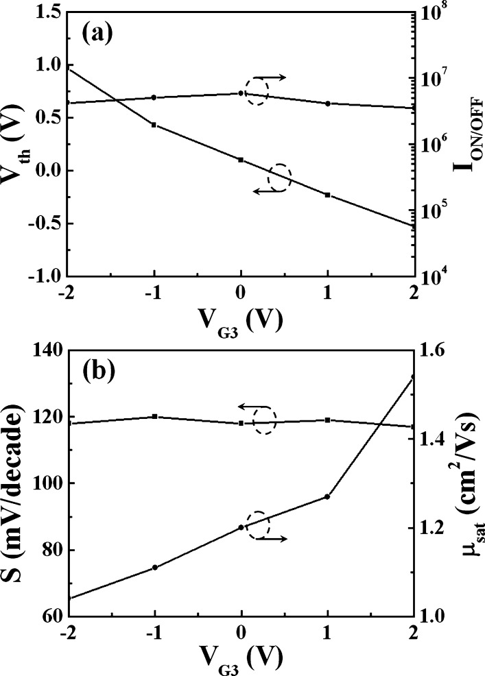
The threshold voltage and current on/off ratio are shown in Figure 4a, where the threshold voltage decreases with increasing secondary gate (G3) voltage. However, the current on/off ratio remains constant at different secondary gate (G3) voltages. The field-effect mobilities and subthreshold swings are shown in Figure 4b, where the field-effect mobility decreases from 1.54 to 1.04 cm2/Vs when the secondary gate (G3) voltage decreases from 2.0 to −2.0 V. However, the subthreshold swing remains a constant at different secondary gate (G3) voltages, which indicates that the subthreshold swing was hardly affected by the secondary gate (G3) voltage.
Figure 4.
(a) Vth and Ion/off ratio of such DGTFTs on paper substrates at different VG3. (b) μ and S of such DGTFTs on paper substrates at different VG3.
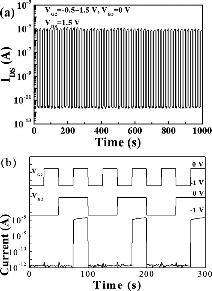
In order to find out whether electrochemical doping existed in the ITO channel layer during the fabrication process, low-frequency pulse respond characteristic is shown in Figure 5a. The current on/off ratio remains a constant of ∼107 without on current decrease, which indicates that no chemical doping or chemical reaction occurs at the chitosan/ITO interface because IDS would decrease after gate scanning when chemical doping or chemical reaction occurred.19 To demonstrate the logic function of such junctionless DGTFTs, different voltage pulse sequences were applied on the dual in-plane gates used as inputs and the drain/source current IDS used as the output, which are shown in Figure 5b, where −1 and 0 V are defined as the low and high levels for the input, respectively. When the high level (0 V) was applied on the dual in-plane gates at the same time, the drain/source current flows, which means the device is ON. Otherwise, the drain/source current is blocked, which means the device is OFF. This is exactly AND logic function, and the current on/off ratio remains a constant of ∼106 without on current decrease.
Figure 5.
(a) Low-frequency pulse respond characteristic of the device with VG2 = −0.5 to 1.5 V, VG3 = 0 V, and VDS = 1.5 V. (b) AND logic function with a large Ion/off.
3. Conclusions
In conclusion, the dual-input AND logic gate based on a single DGTFT was experimentally demonstrated. The dual-gate electrostatic modulation and low-voltage operation mechanism of the junctionless DGTFTs on paper substrates were studied. The threshold voltage of such junctionless DGTFTs could be effectively modulated from negative (−0.53 V) to positive (0.97 V) when the secondary gate (G3) voltage changed from 2.0 to −2.0 V. Such junctionless DGTFTs on paper substrates with AND logic function are very potential for paper sensor applications.
4. Experimental Section
The paper substrates used for oxide-based TFT arrays were ink-jet printing papers. Radio-frequency (RF) magnetron sputtering and plasma-enhanced chemical vapor deposition were used for the fabrication of junctionless paper TFTs gated by solution-processed chitosan dielectrics. The entire process was performed at room temperature. First, a 2.0 μm microporous SiO2 film was deposited on paper substrates for surface passivation, the performance of TFTs can be improved by the smooth surface and interface of paper substrates.20 Second, a 200 nm ITO film was deposited on passivated paper substrates by RF magnetron sputtering at 0.5 Pa. Third, the dielectric layer was fabricated by chitosan solution (2 wt % in acetic acid) and dried in ambient air. At last, ITO source/drain and dual in-plane gate electrodes were completed by RF sputtering through a nickel shadow mask. Electrical characterizations of the junctionless paper TFTs and chitosan dielectric were performed by an impedance analyzer (Agilent 4294A) and a semiconductor parameter analyzer (Keithley 4200 SCS).
Author Contributions
Thin-film transistor and device performance was fabricated and characterized by W.D. The manuscript was prepared by W.D and Y.T. W.D examined and commented on the manuscript. The project was guided by W.D.
The authors declare no competing financial interest.
References
- Luo F. C.; Chen I.; Genovese F. C. A thin-film transistor for flat planel displays. IEEE Trans. Electron Devices 1981, 28, 740–743. 10.1109/t-ed.1981.20422. [DOI] [Google Scholar]
- Spijkman M.-J.; Myny K.; Smits E. C. P.; Heremans P.; Blom P. W. M.; de Leeuw D. M. Dual-gate thin-film transistors, integrated circuits and sensors. Adv. Mater. 2011, 23, 3231–3242. 10.1002/adma.201101493. [DOI] [PubMed] [Google Scholar]
- Guo Y.; Yu G.; Liu Y. Functional organic field-effect transistors. Adv. Mater. 2010, 22, 4427–4447. 10.1002/adma.201000740. [DOI] [PubMed] [Google Scholar]
- Xia F.; Farmer D. B.; Lin Y.-m.; Avouris P. Graphene field-effect transistors with high on/off current ratio and large transport band gap at room temperature. Nano Lett. 2010, 10, 715–718. 10.1021/nl9039636. [DOI] [PubMed] [Google Scholar]
- Zan H.-W.; Chen W.-T.; Yeh C.-C.; Hsueh H.-W.; Tsai C.-C.; Meng H.-F. Dual gate indium-gallium-zinc-oxide thin film transistor with an unisolated floating metal gate for threshold voltage modulation and mobility enhancement. Appl. Phys. Lett. 2011, 98, 153506. 10.1063/1.3578403. [DOI] [Google Scholar]
- Park Y. M.; Salleo A. Dual-gate organic thin film transistors as chemical sensors. Appl. Phys. Lett. 2009, 95, 133307. 10.1063/1.3242372. [DOI] [Google Scholar]
- Colinge J.-P.; Lee C.-W.; Afzalian A.; Akhavan N. D.; Yan R.; Ferain I.; Razavi P.; O’Neill B.; Blake A.; White M.; Kelleher A.-M.; McCarthy B.; Murphy R. Nanowire transistors without junctions. Nat. Nanotechnol. 2010, 5, 225–229. 10.1038/nnano.2010.15. [DOI] [PubMed] [Google Scholar]
- Lee C.-W.; Afzalian A.; Akhavan N. D.; Yan R.; Ferain I.; Colinge J.-P. Junctionless multigate field-effect transistor. Appl. Phys. Lett. 2009, 94, 053511. 10.1063/1.3079411. [DOI] [Google Scholar]
- Lee C.-W.; Nazarov A. N.; Ferain I.; Akhavan N. D.; Yan R.; Razavi P.; Yu R.; Doria R. T.; Colinge J.-P. Low subthreshold slope in junctionless multigate transistors. Appl. Phys. Lett. 2010, 96, 102106. 10.1063/1.3358131. [DOI] [Google Scholar]
- Tobjörk D.; Österbacka R. Paper electronics. Adv. Mater. 2011, 23, 1935–1961. 10.1002/adma.201004692. [DOI] [PubMed] [Google Scholar]
- Dou W.; Jiang J.; Sun J.; Zhou B.; Wan Q. Low-voltage electric-double-layer TFTs on SiO2-covered paper substrates. IEEE Electron Device Lett. 2011, 32, 1543–1545. 10.1109/led.2011.2163811. [DOI] [Google Scholar]
- Fortunato E.; Correia N.; Barquinha P.; Pereira L.; Goncalves G.; Martins R. High-performance flexible hybrid field-effect transistors based on cellulose fiber paper. IEEE Electron Device Lett. 2008, 29, 988–990. 10.1109/led.2008.2001549. [DOI] [Google Scholar]
- Lim W.; Douglas E. A.; Norton D. P.; Pearton S. J.; Ren F.; Heo Y.-W.; Son S. Y.; Yuh J. H. Low-voltage indium gallium zinc oxide thin film transistors on paper substrates. Appl. Phys. Lett. 2010, 96, 053510. 10.1063/1.3309753. [DOI] [Google Scholar]
- Lee J.; Kaake L. G.; Cho J. H.; Zhu X.-Y.; Lodge T. P.; Frisbie C. D. Ion Gel-Gated Polymer Thin-Film Transistors: Operating Mechanism and Characterization of Gate Dielectric Capacitance, Switching Speed, and Stability. J. Phys. Chem. C 2009, 113, 8972–8981. 10.1021/jp901426e. [DOI] [Google Scholar]
- Sun J.; Wan Q.; Lu A.; Jiang J. Low-voltage electric-double-layer paper transistors gated by microporous SiO2 processed at room temperature. Appl. Phys. Lett. 2009, 95, 222108. 10.1063/1.3270001. [DOI] [Google Scholar]
- Jiang J.; Sun J.; Dou W.; Zhou B.; Wan Q. In-plane-gate indium-tin-oxide thin-film transistors self-assembled on paper substrates. Appl. Phys. Lett. 2011, 98, 113507. 10.1063/1.3567946. [DOI] [Google Scholar]
- Spijkman M.; Smits E. C. P.; Blom P. W. M.; de Leeuw D. M.; Bon Saint Côme Y.; Setayesh S.; Cantatore E. Increasing the noise margin in organic circuits using dual gate field-effect transistors. Appl. Phys. Lett. 2008, 92, 143304. 10.1063/1.2904624. [DOI] [Google Scholar]
- Spijkman M.-J.; Brondijk J. J.; Geuns T. C. T.; Smits E. C. P.; Cramer T.; Zerbetto F.; Stoliar P.; Biscarini F.; Blom P. W. M.; de Leeuw D. M. Dual-gate organic field-effect transistors as potentiometric sensors in aqueous solution. Adv. Funct. Mater. 2010, 20, 898–905. 10.1002/adfm.200901830. [DOI] [Google Scholar]
- Herlogsson L.; Crispin X.; Robinson N. D.; Sandberg M.; Hagel O.-J.; Gustafsson G.; Berggren M. Low-voltage polymer field-effect transistors gated via a proton conductor. Adv. Mater. 2007, 19, 97–101. 10.1002/adma.200600871. [DOI] [Google Scholar]
- de Souza M. M.; Jejurikar S.; Adhi K. P. Impact of aluminum nitride as an insulator on the performance of zinc oxide thin film transistors. Appl. Phys. Lett. 2008, 92, 093509. 10.1063/1.2890034. [DOI] [Google Scholar]


