Abstract
Crystalline, electrically conductive, and intrinsically porous materials are rare. Layered two-dimensional (2D) metal–organic frameworks (MOFs) break this trend. They are porous crystals that exhibit high electrical conductivity and are novel platforms for studying fundamentals of electricity and magnetism in two dimensions. Despite demonstrated applications, electrical transport in these remains poorly understood because of a lack of single crystal studies. Here, studies of single crystals of two 2D MOFs, Ni3(HITP)2 and Cu3(HHTP)2, uncover critical insights into their structure and transport. Conductivity measurements down to 0.3 K suggest metallicity for mesoscopic single crystals of Ni3(HITP)2, which contrasts with apparent activated conductivity for polycrystalline films. Microscopy studies further reveal that these MOFs are not isostructural as previously reported. Notably, single rods exhibit conductivities up to 150 S/cm, which persist even after prolonged exposure to ambient conditions. These single crystal studies confirm that 2D MOFs hold promise as molecularly tunable platforms for fundamental science and applications where porosity and conductivity are critical.
Short abstract
A single crystal conductive metal−organic frameworks device and its metallic conduction.
Introduction
Metal–organic frameworks (MOFs) are hybrid inorganic/organic crystals that can possess features distinct from many crystalline materials:1,2 intrinsic porosity, nanometer-scale lattice parameters, flexible mechanics, and a rich structural and compositional diversity enabled by advances in both organic and inorganic chemistry in three dimensions. The vast majority of MOFs are insulators and have been used in applications that benefit from high surface areas and a chemical tunability, such as gas capture and catalysis.1 Conductive MOFs3,4 represent a new type of hybrid inorganic/organic conductor in addition to nonporous coordination polymers and hybrid perovskites, which have recently demonstrated high conductivities and superconductivity5 and promising performances for optoelectronics,6 respectively.
Two-dimensional (2D) layered MOFs,7−19 where metals and redox-active ligands form extended π–d conjugated sheets (Figure 1), have shown the highest conductivities and are predicted to exhibit rare transport phenomena including, for instance, the quantum anomalous hall effect.11 However, because of poor synthetic control and small crystallite size, charge transport and structural studies for the 2D MOFs have generally relied on polycrystalline films/pellets and powder X-ray diffraction (PXRD), where grain boundaries and anisotropy obscure the intrinsic properties. Only a handful of single crystal devices have been reported including a room-temperature conductivity value for a 2D MOF,19 for a 2D coordination polymer,20 and for some less-conductive three-dimensional (3D) MOFs.21,22 Despite Ni3(2,3,6,7,10,11-hexaiminotriphenylene)2 (Ni3(HITP)2) possessing one of the highest conductivities for a porous MOF and having demonstrated promise for various applications, its conduction is poorly understood; calculations have predicted Ni3(HITP)2 to be metallic, but results of experiments on polycrystalline pellets down to 80 K have been interpreted as semiconducting.8,23 Here, with isolated crystals, we reveal the distinct layer stacking for Ni3(HITP)2 and Cu3(2,3,6,7,10,11-hexahydroxytriphenylene)2 (Cu3(HHTP)2), the metallic nature of single crystals of Ni3(HITP)2, and the importance of transport in the out-of-plane direction despite the presumed dominance of in-plane transport for 2D MOFs.
Figure 1.
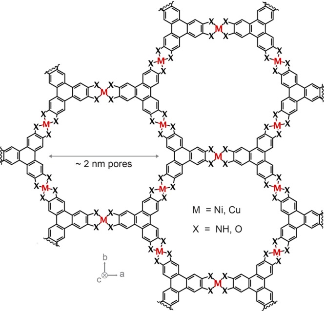
Porous, conductive 2D MOFs. Schematic illustrating the general structure of conductive 2D MOFs where layers stack in the c direction to form intrinsically porous crystals with pores of approximately 2 nm in diameter. Metal atoms and organic ligands comprise the honeycomb lattice of the 2D layers. Ni3(HITP)2 and Cu3(HHTP)2 have M/X = Ni/NH and Cu/O respectively.
Results and Discussion
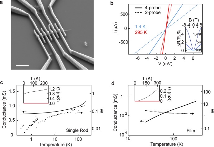
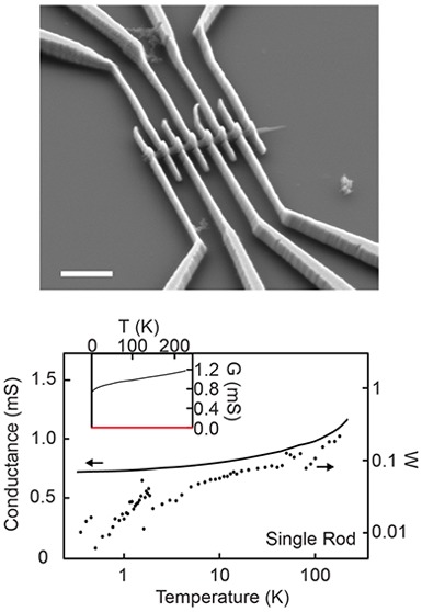
To understand charge transport in our 2D MOFs, we isolated individual crystals of Ni3(HITP)2 and measured their conductivity as a function of temperature (Figure 2). Published conditions8 generate an interconnected nanocrystalline morphology (Figure S1), which has been challenging to isolate crystals from. Here, we obtain isolated rods of Ni3(HITP)2 up to ∼2 μm in length and ∼200 nm in diameter (see Methods and Figure S1). Devices were fabricated by drop-casting suspensions of Ni3(HITP)2 rods onto Si covered by SiO2 substrates and using electron-beam lithography and metal evaporation to deposit Ti/Pd contacts on top of the rods (Figure 2a; see Methods). A DC current–voltage (I–V) sweep for a representative device (Figure 2b) yielded four-probe conductance values G of 1.3 mS at 295 K and 0.7 mS at 1.4 K, and two-probe values of 0.25 mS at 295 K and 0.13 mS at 1.4 K. The linearity observed in these DC measurements even at small biases evinces ohmic contacts over this temperature range and validates the use of AC transport measurements for variable temperature (VT) and magnetic field-dependence studies. A reversible decrease in conductance is observed when a magnetic field is applied (Figure 2b, inset), and the magnitude of this change decreases as the temperature T increases from 1.4 K (top) to 10 K (bottom). The positive magnetoresistance that is enhanced at low temperature suggests a shrinking of electronic impurity wave function under a magnetic field.24 However, because our current device geometry allows for potential mixing between Hall and longitudinal resistance, pinning the exact origin of this behavior will require multiterminal magnetotransport studies in the future.
Figure 2.
Conductive 2D MOF devices of Ni3(HITP)2. (a) SEM of a single rod Ni3(HITP)2 device with Ti/Pd contacts. Scale bar, 1 μm. (b) Current–voltage plots of a single rod Ni3(HITP)2 device at 295 K (red) and 1.4 K (blue). Inset: Normalized magnetoresistance at several fixed temperatures. (c, d) 4-probe temperature-dependent conductance (solid line; left axis) of a single rod device (c) and a polycrystalline film device (d) of Ni3(HITP)2 and their corresponding Zabrodskii plots with their reduced activation energy (dotted lines; right axes). Inset: Temperature-dependent conductance plotted with linear axes.
We find that further decreasing the temperature from 1.4 to 0.3 K (Figure 2c; solid line, left axis) decreased the four-probe conductance negligibly. VT measurements on three additional Ni3(HITP)2 rod devices showed a similar weak, positive dependence on temperature (Figure S2). In contrast, a four-probe VT measurement of a polycrystalline Ni3(HITP)2 film device (Figure 2d; black solid line, left axis) revealed a conductance that decreased by orders of magnitude over a smaller temperature range.
To understand the VT behavior for these single rod and polycrystalline devices, we plot W(T) = d ln G/d ln T against T in a logarithmic scale as shown in Figure 2c,d (dashed lines, right axes). This Zabrodskii plot scheme25 has been used for doped organic polymers,26 quantum dot films,27 and other systems,28,29 where the negative slope of the Zabrodskii plot indicates localization behaviors with a reduced activation gap. We observe a positive slope for all single rod devices, indicating metallicity in the absence of the strong localization at low temperatures. A small reduced activation energy value that decreases as temperature decreases is consistent with a nonzero conductance value as T goes to 0 K (Figure 2c inset). For the polycrystalline film device, we observe a negative slope in the Zabrodskii plot, indicating a semiconducting nature, where the conductance approaches 0 as T goes to 0 K (Figure 2d inset). Literature precedence27−29 and additional data (Figure S3 and S4) are consistent with our interpretation of metallicity or degenerate doping in Ni3(HITP)2 (see Supplementary Discussion).
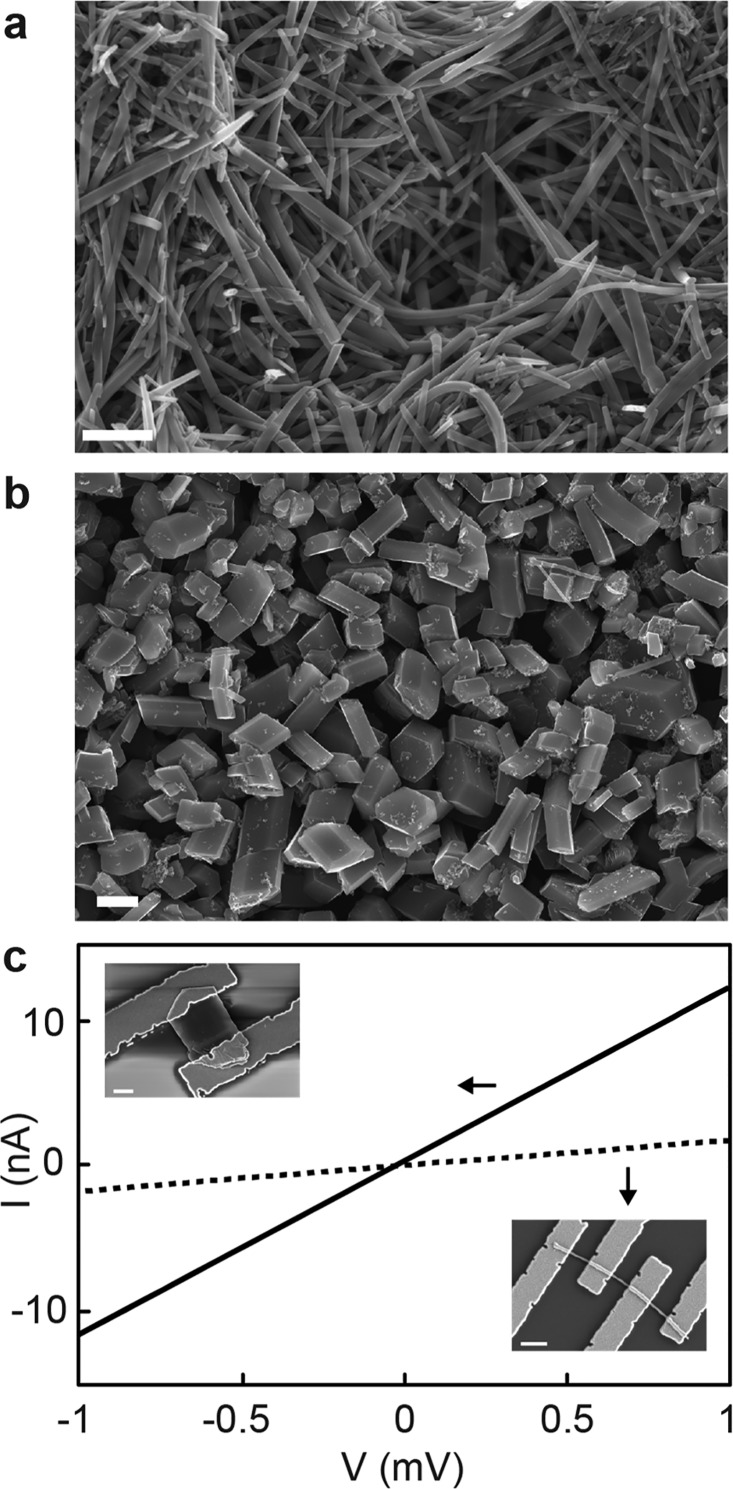
We also isolated individual crystals of Cu3(HHTP)2 and measured their conductivities as previous reports have indicated Cu3(HHTP)2 to be isostructural to Ni3(HITP)2.18 For Cu3(HHTP)2, thin nanocrystalline films18 or rods with diameters of ∼100 nm have been reported.19 Here, we obtain rods (Figure 3a) or particles (Figure 3b) of Cu3(HHTP)2 with six-sided cross sections whose widths can be controlled synthetically (see Methods) from 100 nm up to 5 μm (Figure S5). We also obtain thin flakes of Cu3(HHTP)2 via techniques used to exfoliate traditional 2D materials. Sonication of washed Cu3(HHTP)2 powder in isopropanol, water, or acetonitrile for 1–2 h, followed by centrifugation and isolation of the suspended blue supernatant yields flakes with widths of ∼1 μm, and heights of ∼50–500 nm as evidenced by scanning electron microscope (SEM) and atomic force microscope (AFM) (Figure S6).
Figure 3.
Cu3(HHTP)2. (a, b) SEM images of Cu3(HHTP)2 rods (a) and particles (b) obtained using distinct synthetic conditions (see Methods). Scale bars, 1 μm. (c) Room temperature I–V curves of an exfoliated Cu3(HHTP)2 flake (solid line) and Cu3(HHTP)2 rod (dashed line) at 295 K. Insets show SEM images for corresponding devices.
I–V curves for Cu3(HHTP)2 rod and exfoliated flake devices (Figure 3c), whose SEM images are shown as insets, yielded resistances of 562 kΩ and 84 kΩ at 295 K, allowing us to estimate conductivities of 1.5 S/cm and 0.5 S/cm, respectively, for these devices (Figure S7). Pellet conductivities of 0.1 S/cm and 0.09 S/cm were obtained from the Cu3(HHTP)2 batch of particles used to exfoliate flakes, and the Cu3(HHTP)2 rod batch, respectively. We note that we observe more variability in conductivity for Cu3(HHTP)2 devices than for Ni3(HITP)2 devices, which is likely related to difficulties with reliably forming ohmic contacts to Cu3(HHTP)2, as indicated by the nonlinear I–V curves observed for some devices as well as a significant decrease in conductance from 300 to 200 K, which prevents low temperature characterization. Despite the contact variability, over 10 single rod devices for Cu3(HHTP)2 from different synthetic batches put a lower limit of conductivity at ∼0.1 S/cm and indicate that in-plane and out-of-plane conductivities are of comparable orders of magnitude.
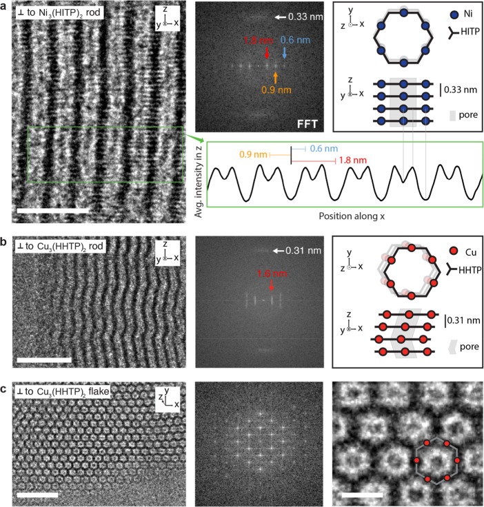
We performed high resolution (HR) TEM on individual crystals of Ni3(HITP)2 and Cu3(HHTP)2 to characterize their respective lattice structures, revealing key new insights into the stacking of 2D layers. These and other triphenylene-based MOFs have been reported to be nearly isostructural based on similarities in PXRD patterns, but the true nature of the stacking remained unclear.18 Imaging perpendicular to the long axis of a Ni3(HITP)2 rod (Figure 4a, left) reveals contrast fringes that run approximately parallel to the rod’s axis. The fast Fourier transforms (FFTs) for this rod (Figure 4a, middle) and others (Figure S8) show the fringe periodicity to be 1.8 nm (red arrows), 0.9 nm (orange arrow), and 0.6 nm (blue arrow). Further inspection indicates an additional periodic feature (diffuse spot) with a spacing of 0.33 nm (white arrow) but with an orientation that is nearly perpendicular to the 1.8 nm family of fringes. The orthogonality of these spots in the FFT, combined with the periodic intensity profile (Figure 4a, bottom) across the width of the rod, suggests that the 2D layers stack in an eclipsed or near-eclipsed configuration, which we illustrate schematically in Figure 4a, right. Specifically, the darker fringes (global minima in intensity profile) correspond to electron scattering along a higher metal and ligand density pathway, and the brighter fringes (local minima) to a lower density scattering pathway along the pore’s center. The brightest fringes (global maxima) arise from scattering along vectors completely free of metal (Ni) atoms. PXRD and additional TEM data from other zone axis (Figure S9), which show 1.1 nm spaced fringes and a hexagonal lattice, support this structural model (Figure 4a).
Figure 4.
TEM of Ni3(HITP)2 and Cu3(HHTP)2. (a) Left: HRTEM image of a Ni3(HITP)2 rod whose long axis lies along the z-direction. Middle: FFT from a lower-magnification TEM image. Right: Schematic of Ni3(HITP)2 structure illustrated for four layers in a near-eclipsed stacking configuration for imaging perpendicular (top schematic) and parallel (bottom schematic) to the 2D layers. Bottom: average intensity in the z-direction measured along the x-direction from the green box in the HRTEM image. The periodic features seen in the FFT are indicated with the red, orange, and blue lines. The gray lines extending from the intensity profile to the schematic indicate the pathways giving rise to the observed intensity profile. Scale bar, 5 nm. (b) Left: HRTEM image of a Cu3(HHTP)2 rod whose long axis lies along the z-direction. Middle: FFT from a lower-magnification TEM image. Right: Schematic of the Cu3(HHTP)2 structure illustrated for four layers in a near-eclipsed stacking configuration for imaging perpendicular (top schematic) and parallel (bottom schematic) to the 2D layers. The three top layers are depicted as stacked with an offset along the same direction, while the bottom layer is stacked with an offset in the opposite direction, and represents a stacking fault. Scale bar, 10 nm. (c) Low- (left) and high-magnification (right) HRTEM image of Cu3(HHTP)2 flake obtained after exfoliation of Cu3(HHTP)2 particles. Scale bars, 10 nm (left) and 2 nm (right).
Surprisingly, HRTEM imaging perpendicular to the long axis of a Cu3(HHTP)2 crystal, previously reported as isostructural with Ni3(HITP)2,18 and FFT analysis (Figure 4b; Figure S10) reveals a critical difference in the nature of stacking in Cu3(HHTP)2 compared to that of Ni3(HITP)2. That is, the eclipsed stacking model does not fit. For Cu3(HHTP)2, the 2D layers are oriented horizontally and perpendicular to the rod axis (i.e., stacked from top to bottom in Figure 4b, left), evidenced by the vertical position of the 0.31 spots in the FFT (white arrow). However, the angled orientation of the bright fringes in the HRTEM images indicates that the 2D layers are not oriented perpendicular to the pores axis. HRTEM and FFTs from other Cu3(HHTP)2 rods (Figure S11) confirm this finding and suggest that the stacking orientation is tilted approximately 15−23° from a direction perpendicular to the pore axis. We propose that angled pores can arise by stacking subsequent layers with an offset along the same a/b direction (Figure 4b, right). Furthermore, the back-and-forth undulating nature of the pores observed in some rods (Figure 4b, left) and the smearing of spots into lines in their respective FFTs (Figure 4b, middle) can be explained by stacking faults or twin defects, as shown schematically with the bottom layer (Figure 4b, right and Figure S10). Such defects would give rise to reversals in the stacking offset direction and thus an undulating appearance. Additional data are consistent with this model where layers and pores are not perpendicular because of noneclipsed stacking. First, SEM images of larger, faceted rods show six-sided cross sections that are not perpendicular to the rod’s long axis, with clean cleavage planes that are similarly not normal to the rod’s long axis (Figure S12). Second, synchrotron PXRD data of Cu3(HHTP)2 (Figure S13) do not fit well with an eclipsed hexagonal unit cell but rather by a structure similar to the one outlined above (Figure 4b, right). Third, TEM images (Figure 4c, left) and FFTs (Figure 4c, middle) of thin flakes obtained after exfoliation show a hexagonal crystalline structure with a honeycomb pattern that is consistent with imaging parallel to the pore axis (∼20° from the z-direction).
Further analysis and literature precedent suggest new insights into the 2D layer stacking that may be relevant to the growth, transport, and calculations thereof for 2D MOFs generally. The diffuse nature of the interlayer spots in the FFT for Ni3(HITP)2 (white arrow; Figure 4a, middle) and the range of pore angles for some Cu3(HHTP)2 rods (Figure 4b, middle) are consistent with a variation in the stacking offset between layers and may indicate that a strict assignment of AA or AB stacking with a single offset value may not fully capture the structural features normal to the 2D MOF plane. Furthermore, the pores can stay continuous over hundreds of nanometers despite significant stacking variation over that length scale, indicating that the 2D layers are strongly ordered locally, where each subsequent layer is only offset by a small fraction of the 2D lattice’s unit cell. This is consistent with previous calculations for Ni3(HITP)2,8 which predict a shallow potential energy surface for various stacking configurations that are near but not perfectly eclipsed (Figures S8 and S10).
With the aid of single crystal device data, we make observations relevant to understanding transport in conductive 2D MOFs. First, for both Cu3(HHTP)2 and Ni3(HITP)2 systems, rod devices with significant out-of-plane contributions show conductivities greater than their polycrystalline pellet measurements. The out-of-plane transport is often disregarded in the literature compared to in-plane transport30 but is consistent with band structure and density of states calculations, which show that C, N, and Ni contribute to these out-of-plane bands. Second, Zabrodskii plots show a positive slope for single crystal Ni3(HITP)2 devices but a negative slope for its polycrystalline film, indicating the intrinsic metallic nature for single crystal MOFs, with the observed nonmetallic behavior of polycrystalline film likely extrinsic to the materials. Additional work is needed to further understand the role that anisotropy and grain boundaries contribute to polycrystalline transport. Importantly, for organic systems and quantum dot films, by controlling film preparation and the material’s surface, conductance can be increased by orders of magnitude; similar strategies may yield significant increases in polycrystalline MOF transport. Last, we note that literature reports have attempted to claim metallicity or a semiconducting nature for various MOFs or coordination polymers by analyzing high temperature polycrystalline pellets or by applying Arrhenius equations to weak temperature dependences, which may lead to incorrect interpretations of small band gaps. We show that, although the out-of-plane conduction for Ni3(HITP)2 devices decreases with temperature, the Zabrodskii analysis at low temperatures and single crystals are critical in determining the nature of its conduction.
Acknowledgments
Work in the Dincă lab was supported by the Army Research Office (Grant No. W911NF-17-1-0174). P.K. acknowledges the support from ONR MURI (N00014-16-1-2921) for electrical transport measurement and ARO (W911NF-18-1-0366) for device fabrication. N.C.G. acknowledges support from ARO (W911NF-181-0359). I.S. is grateful to the Belgian American Educational Foundation (BAEF) and Research Foundation – Flanders (FWO) for postdoctoral fellowships. Computational work used the Extreme Science and Engineering Discovery Environment (XSEDE), which is supported by the National Science Foundation Grant No. ACI-1548562, and the PICS machine, Coeus, which is supported by the NSF (DMS1624776). TEM characterization was performed in the EPIC facility of Northwestern University’s NUANCE Center, which has received support from the Soft and Hybrid Nanotechnology Experimental (SHyNE) Resource (NSF ECCS-1542205); the MRSEC program (NSF DMR-1121262) at the Materials Research Center; the International Institute for Nanotechnology (IIN); the Keck Foundation; and the State of Illinois, through the IIN. Part of this work was performed at the Center for Nanoscale Systems (CNS), a member of the National Nanotechnology Coordinated Infrastructure Network, which is supported by the National Science Foundation under NSF award #1541959. CNS is part of Harvard University.
Supporting Information Available
The Supporting Information is available free of charge at https://pubs.acs.org/doi/10.1021/acscentsci.9b01006.
Material preparation and characterization, device fabrication and characterization, band structure calculations, and growth and device discussions (PDF)
The authors declare no competing financial interest.
Supplementary Material
References
- Furukawa H.; et al. The Chemistry and Applications of Metal-Organic Frameworks. Science 2013, 341, 1230444. 10.1126/science.1230444. [DOI] [PubMed] [Google Scholar]
- Coudert F.-X. Responsive Metal-Organic Frameworks and Framework Materials: Under Pressure, Taking the Heat, in the Spotlight, with Friends. Chem. Mater. 2015, 27, 1905–1916. 10.1021/acs.chemmater.5b00046. [DOI] [Google Scholar]
- Stassen I.; et al. An Updated Roadmap for the Integration of Metal-Organic Frameworks with Electronic Devices and Chemical Sensors. Chem. Soc. Rev. 2017, 46, 3185–3241. 10.1039/C7CS00122C. [DOI] [PubMed] [Google Scholar]
- Sun L.; Campbell M. G.; Dincă M. Electrically Conductive Porous Metal-Organic Frameworks. Angew. Chem., Int. Ed. 2016, 55, 3566. 10.1002/anie.201506219. [DOI] [PubMed] [Google Scholar]
- Huang X.; et al. Superconductivity in a Copper(II)-Based Coordination Polymer with Perfect Kagome Structure. Angew. Chem., Int. Ed. 2018, 57, 146–150. 10.1002/anie.201707568. [DOI] [PubMed] [Google Scholar]
- Li W.; Wang Z.; Deschler F.; Gao S.; Friend R. H.; Cheetham A. K. Chemically Diverse and Multifunctional Hybrid Organic-Inorganic Perovskites. Nat. Rev. Mater. 2017, 2, 16099. 10.1038/natrevmats.2016.99. [DOI] [Google Scholar]
- Ko M.; Mendecki L.; Mirica K. Conductive Two-Dimensional Metal-Organic Frameworks as Multifunctional Materials. Chem. Commun. 2018, 54, 7873–7891. 10.1039/C8CC02871K. [DOI] [PubMed] [Google Scholar]
- Sheberla D.; et al. High Electrical Conductivity in Ni3(2,3,6,7,10,11- hexaiminotriphenylene)2, a Semiconducting Metal-Organic Graphene Analogue. J. Am. Chem. Soc. 2014, 136, 8859–8862. 10.1021/ja502765n. [DOI] [PubMed] [Google Scholar]
- Dou J.-H.; et al. Signature of Metallic Behavior in the Metal-Organic Frameworks M3(hexaiminobenzene)2. J. Am. Chem. Soc. 2017, 139, 13608–13611. 10.1021/jacs.7b07234. [DOI] [PubMed] [Google Scholar]
- Campbell M. G.; et al. Cu3(hexaiminotriphenylene)2: an Electrically Conductive 2D Metal-Organic Framework for ChemiresistiveSensing. J. Am. Chem. Soc. 2015, 137, 13780. 10.1021/jacs.5b09600. [DOI] [PubMed] [Google Scholar]
- Dong L.; et al. Two-Dimensional π-Conjugated Covalent-Organic Frameworks as Quantum Anomalous Hall Topological Insulators. Phys. Rev. Lett. 2016, 116, 096601. 10.1103/PhysRevLett.116.096601. [DOI] [PubMed] [Google Scholar]
- Dong R.; Zhang Z.; Tranca D. C.; et al. A Coronene-Based Semiconducting Two-Dimensional Metal-Organic Framework with Ferromagnetic Behavior. Nat. Commun. 2018, 9, 2637. 10.1038/s41467-018-05141-4. [DOI] [PMC free article] [PubMed] [Google Scholar]
- Sheberla D.; et al. Conductive MOF Electrodes for Stable Supercapacitors with High Areal Capacitance. Nat. Mater. 2017, 16, 220–224. 10.1038/nmat4766. [DOI] [PubMed] [Google Scholar]
- Feng D.; et al. Robust and Conductive Two-Dimensional Metal-Organic Frameworks with Exceptionally High Volumetric and Areal Capacitance. Nature Energy 2018, 3, 30–36. 10.1038/s41560-017-0044-5. [DOI] [Google Scholar]
- Miner E. M.; Fukushima T.; Sheberla D.; Sun L.; Surendranath Y.; Dincă M. Electrochemical Oxygen Reduction Catalysed by Ni3(hexaiminotriphenylene)2. Nat. Commun. 2016, 7, 10942. 10.1038/ncomms10942. [DOI] [PMC free article] [PubMed] [Google Scholar]
- Dong R.; Han P.; Arora H.; et al. High-Mobility Band-Like Charge Transport in a Semiconducting Two-Dimensional Metal-Organic Framework. Nat. Mater. 2018, 17, 1027–1032. 10.1038/s41563-018-0189-z. [DOI] [PubMed] [Google Scholar]
- Campbell M. G.; Liu S. F.; Swager T. M.; Dincă M. Chemiresistive Sensor Arrays from Conductive 2D Metal-Organic Frameworks. J. Am. Chem. Soc. 2015, 137, 13780–13783. 10.1021/jacs.5b09600. [DOI] [PubMed] [Google Scholar]
- Rubio-Giménez V.; et al. Bottom-Up Fabrication of Semiconductive Metal-Organic Framework Ultrathin Films. Adv. Mater. 2018, 30, 1704291. 10.1002/adma.201704291. [DOI] [PubMed] [Google Scholar]
- Hmadeh M.; et al. New Porous Crystals of Extended Metal-Catecholates. Chem. Mater. 2012, 24, 3511–3513. 10.1021/cm301194a. [DOI] [Google Scholar]
- Kambe T.; et al. Redox Control and High Conductivity of Nickel Bis(dithiolene) Complex π-Nanosheet: A Potential Organic Two-Dimensional Topological Insulator. J. Am. Chem. Soc. 2014, 136, 14357–14360. 10.1021/ja507619d. [DOI] [PubMed] [Google Scholar]
- Aubrey M.; et al. Electron Delocalization and Charge Mobility as a Function of Reduction in a Metal-Organic Framework. Nat. Mater. 2018, 17, 625–632. 10.1038/s41563-018-0098-1. [DOI] [PubMed] [Google Scholar]
- Xie L. S.; et al. Tunable Mixed-Valence Doping toward Record Electrical Conductivity in a Three-Dimensional Metal-Organic Framework. J. Am. Chem. Soc. 2018, 140, 7411–7414. 10.1021/jacs.8b03604. [DOI] [PubMed] [Google Scholar]
- Foster M. E.; et al. Unraveling the Semiconducting/Metallic Discrepancy in Ni3(HITP)2. J. Phys. Chem. Lett. 2018, 9, 481–486. 10.1021/acs.jpclett.7b03140. [DOI] [PubMed] [Google Scholar]
- Nguen V. L.; Spivak B. Z.; Shklovskii B. I. Tunnel Hops in Disordered Systems. Sov. Phys.-JETP 1985, 62, 1021. [Google Scholar]
- Zabrodskii A. G.; Shlimak I. S. Sov. Phys. Semicond. 1975, 9, 391. [Google Scholar]
- Le T.-H.; Kim Y.; Yoon H. Electrical and Electrochemical Properties of Conducting Polymers. Polymers 2017, 9, 150. 10.3390/polym9040150. [DOI] [PMC free article] [PubMed] [Google Scholar]
- Liu H.; Pourret A.; Guyot-Sionnest P. Mott and Efros-Shklovskii Variable Range Hopping in CdSe Quantum Dots Films. ACS Nano 2010, 4, 5211–5216. 10.1021/nn101376u. [DOI] [PubMed] [Google Scholar]
- Ahlskog M.; Reghu M.; Heeger A. J. The Temperature Dependence of the Conductivity in the Critical Regime of the Metal-Insulator Transition in Conducting Polymers. J. Phys.: Condens. Matter 1997, 9, 4145–4156. 10.1088/0953-8984/9/20/014. [DOI] [Google Scholar]
- Kaiser A. B. Electronic Transport Properties of Conducting Polymers and Carbon Nanotubes. Rep. Prog. Phys. 2001, 64, 1–49. 10.1088/0034-4885/64/1/201. [DOI] [Google Scholar]
- Skorupskii G.; Trump B. A.; Kasel T. W.; Brown C. M.; Hendon C. H.; Dincă M.. Efficient and tunable one-dimensional charge transport in layered lanthanide metal-organic frameworks Nat. Chem., 2019, 11, 10.1038/s41557-019-0372-0 [DOI] [PMC free article] [PubMed] [Google Scholar]
Associated Data
This section collects any data citations, data availability statements, or supplementary materials included in this article.


