Abstract
The long-standing interest in graphene has recently brought graphene-derived materials including graphene hydrogel, graphene fiber and graphene paper into sharp focus. These graphene-derived materials show outstanding properties in mechanics and physics. In this paper, for the first time, we demonstrate the novel synthesis of graphene dendrites on SiO2/Si substrates by chemical vapor deposition. The tree-like graphene dendrites with well-controlled morphology can be directly grown on both the Si and the SiO2 surfaces of the substrates by using methane and hydrogen as precursors. The graphene dendrites on SiO2/Si substrates can be directly used in the fabrication of the electronic device. The conductivity and the Hall mobility of graphene dendrites are ~ 286 Scm−1 and ~ 574 cm2(Vs)−1, respectively. Young’s modulus of graphene dendrites is up to 2.26 GPa. The developed method avoids the need for a metal substrate and is scalable and compatible with the existing semiconductor technology, making graphene dendrites be very promising in nanoelectronic applications.
Keywords: Graphene dendrites, SiO2/Si substrates, CVD, Nanoelectronic applications
Introduction
Graphene is a kind of two-dimensional (2D) crystal material with sp2 carbon atoms arranged in a honeycomb lattice. Because of the excellent physical and chemical properties, graphene has attracted tremendous attention since it was found by mechanical cleavage of highly ordered pyrolytic graphite (HOPG) in 2004 [1]. To date, graphene has been demonstrated to be a very promising material in supercapacitors, solar cells, sensors, and so on [2–10]. At the same time, the graphene-derived materials such as one-dimensional graphene fiber, two-dimensional graphene paper, and three-dimensional graphene hydrogel have also been studied extensively. These graphene-derived materials show novel mechanical and electrical properties quite different from graphene[11–14].
Graphene dendrite is a new type of graphene-derived material, which has a tree-like crystal structure. Generally, the dendrite structure can be formed in a non-equilibrium state during the crystal growth process. To date, a variety of materials such as metal, alloy and metal oxide have been demonstrated to form the dendrite structures [15–18]. These dendrites usually have unique physical and chemical properties, making them have wide applications in many fields. For example, the large specific surface area of the dendrite can enlarge the number of active adsorption sites, which is expected to achieve higher sensitivity for the chemical sensors and biosensors [19–21].
Though the dendrites are the ubiquitous crystal form in freezing alloys and super-cooled melts, the graphene oxide dendrite and graphene dendrite are not synthesized until 2015 [22, 23]. The graphene oxide dendrite was first synthesized by a chemical reaction in several steps, which was demonstrated to be useful in sensing and separation [22]. In the same year, Liu et al. prepared the graphene dendrite by electrochemical reaction using graphene oxide as the precursor. The prepared graphene dendrite showed a conductivity of 44 Sm−1 and was used as the electrode in supercapacitors [23]. However, up to now, the synthesis of graphene dendrites is limited to electrochemical reaction using graphene oxide as the precursor. The conductivity of the synthesized graphene dendrites is still relatively low due to the poor conductance of graphene oxide. Moreover, a metal substrate is indispensable in the electrochemical reaction. As a result, the complicated and skilled post-growth techniques have to be employed to remove metal substrates and transfer the graphene dendrites to dielectric substrates (SiO2/Si or quartz) for fabricating electronic devices [24–26].
In this work, we develop a facile strategy to directly fabricate graphene dendrites on SiO2/Si substrates by chemical vapor deposition (CVD) using methane and hydrogen as precursors. Without using any catalyst, the tree-like graphene dendrites with high density were directly grown on dielectric substrates. This method does not require the metal substrate, and thus is compatible with the fabrication process of electronic device. The fabricated graphene dendrites show a good conductivity of ~ 286 Scm−1, which is about 6.5 times higher than that synthesized by the electrochemical method. The Hall mobility of the graphene dendrites is up to ~ 574 cm2(Vs)−1 by the Hall effect measurement. Moreover, the graphene dendrites show excellent mechanical properties with Young’s modulus up to 2.26 GPa. The developed technique is compatible with the existing semiconductor technology, thus will be very useful in nanoelectronic applications such as biochemical sensors, nano-electromechanical systems, as well as molecular electronics.
Methods
The Growth of Graphene Dendrites
N-type Si wafers with a 300 nm thickness SiO2 layer were used as the substrates. These substrates were sequentially cleaned by acetone, anhydrous ethanol, and deionized water before they were loaded into the CVD reaction system. The detailed experimental apparatus and experimental process are schematically illustrated in Fig. 1. The cleaned substrates were placed on the top-surface of the outer wall of a 2-in. quartz tube, and then the 2 in. quartz tube was placed inside a 3-in. quartz tube in the CVD chamber. The precursor CH4 and H2 were introduced into the CVD reaction system, following the vacuum reached as low as 1 × 10⁻⁴ mbar. The flow rate of CH4 and H2 was 25 sccm and 15 sccm, respectively. As the temperature was increased to more than 950 °C, CH4 began to decompose and deposit on the substrates thus acting as the carbon source for the graphene dendrites. When the growth process was completed, the samples were rapidly cooled down to room temperature at a rate of ~ 100 °C/min by exposing the cube in air. The gas emissions from the CVD reaction system were burned in a pyrolysis furnace and then discharged into the air.
Fig. 1.

Schematic illustration of CVD process for growing graphene dendrites
Characterizations
The morphology of the graphene dendrites on SiO2/Si substrates was characterized utilizing the scanning electron microscopy (SEM, ZEISS, SUPRATM-55). The energy dispersive spectroscopy (EDS) was applied for element analysis of graphene dendrites. X-ray photoelectron spectroscopy (XPS) spectra of the samples were measured using a Thermofisher ESCALAB 250 with monochromatized Al Kα X-ray radiation. The as-grown graphene dendrites were evaluated using a confocal Raman spectroscopy (LabRAM HR800) in a backscattering configuration with a 532 nm laser for excitation. The selected area electron diffraction pattern (SAED) and transmission electron microscopy (TEM) images of graphene dendrites were acquired using transmission electron microscopy (TEM, JEOL JEM2100) with an acceleration voltage at 200 kV. The electrical properties (ISD-VSD characteristics) were measured with a semiconductor parameter analyzer (PDA FS360) coupled with a probe station (PEH-4) at room temperature. The mechanical properties of the graphene dendrites were characterized by Atomic force microscopy (AFM, Bruker Multimode 8) in PeakForce Quantitative Nanomechanical Mapping (PFQNM) mode in air.
Results and Discussion
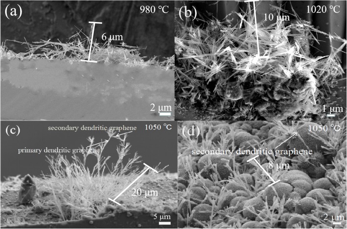
The graphene dendrites were synthesized on the SiO2/Si substrates using a low-pressure CVD system. In this CVD system, the growth parameters of the graphene dendrites can be precisely controlled. Figure 2a–c show graphene dendrites grown on the Si surface of the SiO2/Si substrates at a different temperature from 980 °C to 1050 °C. The growth temperature can greatly affect the configuration and the length of the graphene dendrites. As can be seen in Fig. 2, the graphene dendrites grown at 980 °C are high density and the typical dendrite length is about 6 μm (Fig. 2a). For the graphene dendrites grown at 1020 °C, the typical length of the graphene dendrites is about 10 μm (Fig. 2b). When the growth temperature further increases to 1050 °C, the total length of graphene dendrites increases to about 20 μm (Fig. 2c). Interestingly, we find that graphene dendrites grown at 1050 °C show a typical tree-like structure with many secondary dendrites grown on the top of the primary dendrite structure. The tree-like graphene dendrites also can be grown on SiO2 surface of the SiO2/Si substrates at 1050 °C as shown in Fig. 2d. The length of the tree-like graphene dendrites is typically less than 10 μm. As shown in Fig. 2c, d, graphene dendrites grow along a certain direction, which can be attributed to the anisotropic surface energies of SiO2/Si substrate [27].
Fig. 2.
SEM images of graphene dendrites synthesized on Si surface of the SiO2/Si substrates at the growth temperature of 980 °C (a), 1020 °C (b), and 1050 °C (c), and on SiO2 surface of the SiO2/Si substrates at 1050 °C (d). The growth time was 120 min
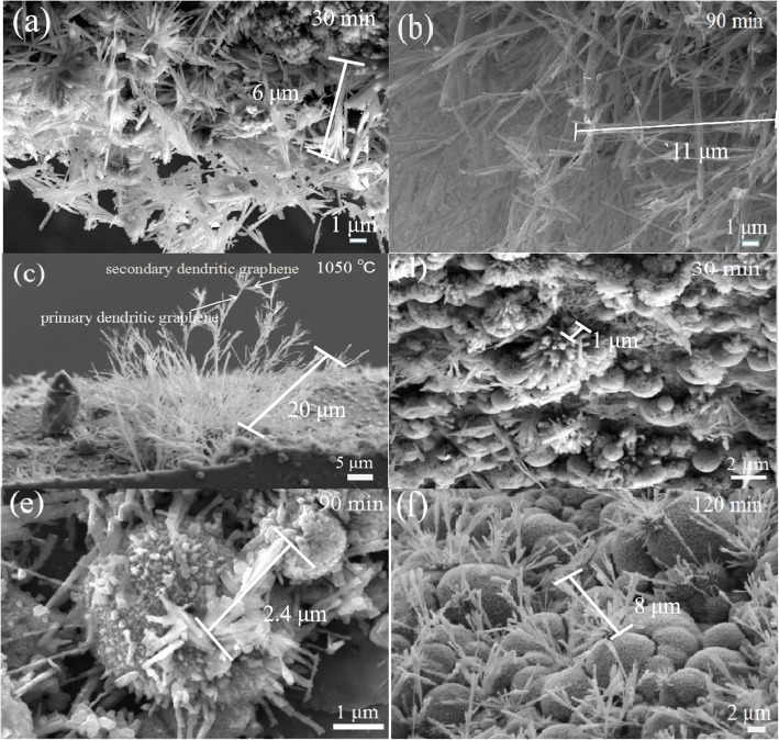
The morphologies of the graphene dendrites are also strongly affected by the growth time. Figure 3 shows SEM images of the graphene dendrites grown at different growth time. As the growth time increases from 30 to 120 min, the length of the tree-like graphene dendrites on the Si surface increases from ~ 6 to ~ 20 μm (Fig. 3a–c), and the length of the dendrites on the SiO2 surface increases from ~ 1 to ~ 8 μm (Fig. 3d–f). As can be seen from Fig. 3, the length of dendrites grown on the Si surface is larger than that grown on the SiO2 surface under the same growth conditions. This phenomenon can be attributed to the fact that the roughness of the Si surface is larger than that of the SiO2 surface, as a polishing process was performed on the SiO2 surface. Generally, the rough substrate has large surface energy [28, 29], which is beneficial for the growth of the graphene dendrites. Moreover, a hetero-structure is expected to form between graphene dendrites and Si surface, as the work function of graphene (4.5~4.8 eV) is higher than that of Si (~ 4.3 eV), which allows electron charge transfer from Si to graphene [30–32].
Fig. 3.
SEM images of tree-like graphene dendrites synthesized on the Si surface (a–c) and on the SiO2 surface (d–f) of the SiO2/Si substrates for the different growth time from 30 to 120 min at 1050 °C
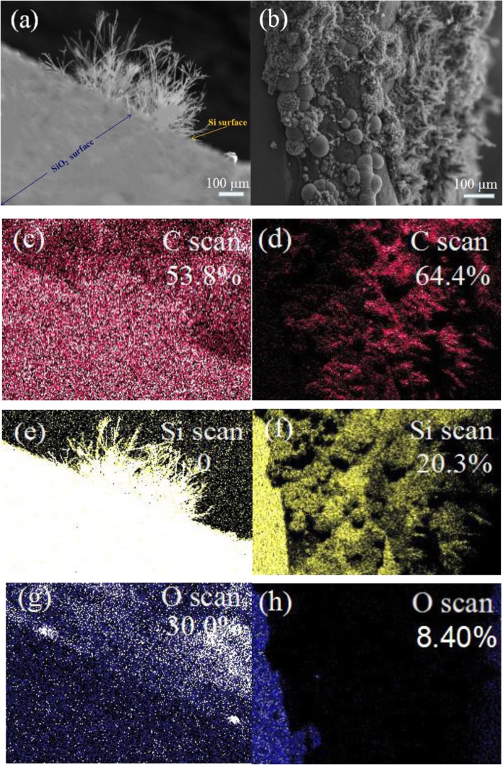
The elemental composition of the samples grown on both Si surface and SiO2 was investigated by EDS. Figure 4a, b show the SEM image areas performed by EDS on both Si and SiO2 surface, respectively. The EDS maps for the elemental C, Si and O of the samples are shown in the Fig. 4c–h. The percentages of the elemental content of the structures are labeled in the right-top EDS scan maps. On both Si and SiO2 surface, elemental C dominates with over half that 53.8% on Si surface and 64.4% on SiO2. A small amount of Si and O elements are also observed (Fig. 4e–h), which are considered to come from SiO2/Si substrates. The EDS result confirms that the elemental composition of the sample is in accordance with that of graphene.
Fig. 4.
SEM images of graphene dendrites grown on the Si surface (a) and SiO2 surface (b). EDS maps of element content of C (c), Si (e), and O (g) scanned in the same area with (a). EDS maps of element content of C (d), Si (f), and O (h) scanned in the same area with (b)
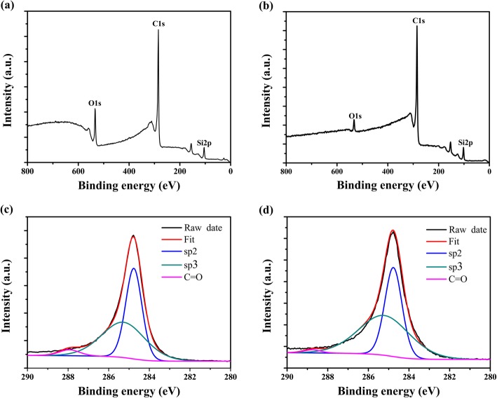
X-ray photoelectron spectroscopy (XPS) was also performed to further illustrate the detail structural characterization of the graphene dendrites prepared on the Si and SiO2 surface of the SiO2/Si substrates (Fig. 5). The peak C1s at about ~ 284 eV is clearly observed on both Si and SiO2 surface, which can be assigned to the sp2 C-C network [33]. The peaks of O1s at ~ 533 eV and Si2p at ~ 104 eV are also observed, which can be assigned to the SiO2/Si substrate [34]. Figure 5c, d show the cure fit of C1s from Fig. 5a, b, respectively. For both cases, the peak C1s can be divided into three peaks. The main peak at ~ 284.7 eV reveals the appearance of sp2 hybridization peak of graphene. The peak at ~ 285.3 eV is assigned to the sp3-hybridization C-C bonding ascribing to the contamination of natural carbon [35]. The weak peak at ~ 288 eV relates to carbon C=O groups, which probably originate from the oxygen contamination during graphene dendrite growth [36].
Fig. 5.
XPS spectra of graphene dendrites grown on SiO2 (a) and Si (b) surface of the SiO2/Si substrates. Curve fit of C1s peak of graphene dendrites grown on SiO2 (c) and Si (d) surface of the SiO2/Si substrates
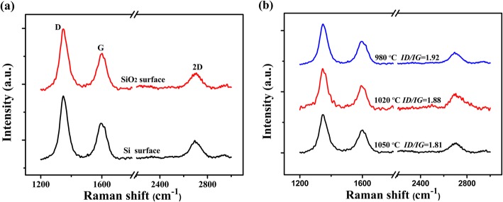
Raman spectra were performed to investigate the crystal quality and the number of layers of the graphene dendrites [37–39]. As shown in Fig. 6a, the D peak (~ 1350 cm−1), G peak (~ 1580 cm−1), and 2D peak (~ 2680 cm−1) of graphene are observed on both Si and SiO2 surface of the SiO2/Si substrates. The G peak is the characteristic of the carbon sp2 structure and the 2D peak is the second order of zone boundary phonons. The D peak is a defect-related peak reflecting the disorder of graphene [40–43]. For the graphene dendrites grown on both Si and SiO2 surface, the intensity of the G peak is much higher than that of the 2D peak, indicating that graphene dendrites grown on both Si and SiO2 surfaces have a multilayered structure. In addition, as the growth temperature increases from 980 to 1050 °C, the peak intensity ratio of ID/IG decreases from 1.92 to1.81, indicating that the quality of the graphene dendrites was improved with the increase of growth temperature (Fig. 6b) [40–43].
Fig. 6.
a Raman spectra of graphene dendrites grown on both Si and SiO2 surface of SiO2/Si substrates. b Raman spectra of grpahene dendrites grown on Si surface from 980 °C to 1050 °C
We further performed TEM and SAED to investigate the detailed structure of graphene dendrites . The samples were transferred to the TEM grid before the TEM imaging. From Fig. 7a, b, we can see that the diameter of the primary and secondary graphene dendrites is about 1 μm and 50 nm, respectively. Figure 7c, d show the SAED patterns from the primary and secondary graphene dendrites, respectively. For both cases, the patterns show a typical 6-fold symmetry of graphene [44, 45]. The high-resolution TEM (HRTEM) images of primary and secondary graphene dendrites taken from the edge of the samples are shown in Fig. 7e, f. For both cases, the HRTEM image shows a multilayer structure, indicating the dendrite is made up of multilayer graphene. This result is consistent with Raman characterization.
Fig. 7.

Low-magnification TEM images of the primary (a) and the secondary (b) graphene dendrites, and the SAED patterns taken from primary (c) and the secondary (d) graphene dendrites, respectively. High-resolution TEM images of primary (e) and the secondary (f) graphene dendrites
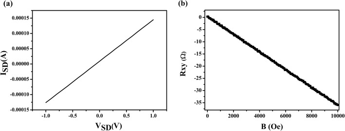
The electrical properties of the graphene dendrites were evaluated with a back-gated field-effect transistor (FET). For the electrical measurement, the samples were placed into a probe station. Two tungsten microprobes (10 μm in diameter) were used as the source and the drain electrodes and placed directly on the SiO2 surface at two ends of several selected samples of graphene dendrites. Figure 8a shows the linear and reproducible ISD-VSD curves at zero gate voltage, demonstrating the ohmic contact obtained between graphene dendrites and tungsten probes. The resistance R of the graphene dendrites is approximately 6110 Ω. The resistivity ρ is obtained via the equation:
| 1 |
Fig. 8.
a A representative current-voltage (ISD-VSD) curves of the graphene dendrites at zero gate voltage. b Hall resistances as a function of magnetic field strength for graphene dendrites
Where the S and L are the cross-section and length of the graphene dendrites. The conductivity σ is calculated by the formula:
| 2 |
Based on the above analysis, the electrical conductivity of the dendrites is ~ 286 Scm−1.
Electronic transport measurements on the SiO2 surface with van der Pauw structure were carried out at room temperature. Hall resistance (Rxy) as a function of the magnetic field strength has been shown in Fig. 8b. Hall coefficient RH is calculated by the formula:
| 3 |
Where t is the thickness of the sample, and Rxy is the longitudinal resistance. Hall coefficient is − 1.2 cm3/C.
The resistivity of the graphene dendrites is extracted by the equations:
| 4 |
Where ρ is the resistivity of the sample, Rxx is the longitudinal resistance, f is the van der Pauw factor, and its value is close to 1 thus neglected. The obtained conductivity is ~ 474 S/cm, which is comparable to the value of ~ 286 Scm−1 measured by FET.
Furthermore, we further calculate the Hall mobility with the following formula:
| 5 |
The Hall mobility of graphene dendrites is calculated to be ~ 574 cm2/Vs, which is much higher than that of the nanocrystalline graphene thin film reported previously [46].
To evaluate the mechanical properties of the graphene dendrites, AFM imaging in PFQNM mode was used to investigate Young’s modulus of the graphene dendrites. The measurements were carried out under ambient conditions at room temperature. Figure 9a shows the data that the force plot as a function of the separation, which represents the interaction of one approaching (green line) and retracting (red line) cycle in PFQNM.
Fig. 9.
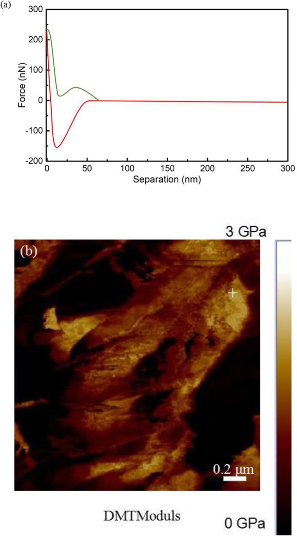
a AFM force-displacement curve of graphene dendrites. b AFM DMT Modulus image of Young’s modulus of graphene dendrites
In order to obtain Young’s modulus, a fit of the retraction curve was implemented using the Derjaguin-Muller-Toporov (DMT) model [47].
| 6 |
where the F-Fadh represents the force on the cantilever relative to the adhesion force, R is the tip end radius, and d is the deformation of the sample. The result of the fit is the reduced modulus E*. Young’s modulus can be calculated by the following equation
| 7 |
where the vs and vtip are Poisson’s ratio of the samples and tip, respectively, the Es and Etip are Young’s modulus the samples and tip, respectively. Sample with a scanning size of 2.0 μm × 2.0 μm was tested. As shown in Fig. 9b, the graphene dendrites are shown in the yellow area of the map. Young’s modulus of graphene dendrites is up to 2.26 GPa obtained from the yellow cross marked region.
We compare the mechanical and electrical properties of different types of graphene-derived materials as shown in Table 1 [11–14, 23]. The conductivity of our graphene dendrite is several orders higher than that of graphene hydrogel and the graphene dendrite produced by the electrochemical method [23]. The value also is comparable to that of the other graphene-derived materials, such as graphene fibers of ~ 10 Scm−1 [12] and 2.5 × 10⁴ Sm−1 (250 Scm-1) [13] and graphene paper of 351 Scm−1 [14]. For the mechanical strength, Young’s modulus of graphene dendrites in this work is much higher than graphene hydrogel of~ 450 kPa (~ 4.5 × 10⁻⁴ GPa), and is also comparable to that of graphene fibers of 420 MPa (0.42 GPa) [12] and ~ 7700 MPa (~ 7.7 GPa) [13]. In comparison with the other graphene-derived materials, the graphene dendrite is more suitable for use in the nanoelectronic device due to nanometer level size in diameter and good compatibility with the existing semiconductor technology.
Table 1.
The mechanical and electrical properties of different types of graphene-derived materials. This table records Young’s modulus and conductivity of different types of graphene-derived materials (graphene hydrogel, graphene fibers, graphene paper, and graphene dendrites)
| Type | Youngʼs modulus | Conductivity | Reference |
|---|---|---|---|
| Graphene hydrogel |
~ 450 kPa (~ 4.5×10⁻⁴ GPa) |
5 × 10⁻³ Scm−1 | [11] |
| Graphene fibers |
420 MPa (0.42 GPa) |
~ 10 Scm−1 | [12] |
| Graphene fibers |
~ 7700 MPa (~ 7.7 GPa) |
~ 2.5 × 10⁴ Sm−1 (250 Scm−1) |
[13] |
| Graphene paper | – | 351 Scm−1 | [14] |
| Graphene dendrite | – |
44 S/m (0.44 Scm−1) |
[23] |
| Graphene dendrite | 2.26 GPa | ~ 286 Scm−1 | This work |
Conclusions
In this work, we have successfully achieved direct growth of graphene dendrites on both Si and SiO2 surfaces on SiO2/Si substrates using a CVD method. The morphology of the graphene dendrites can be regulated by the growth temperature and growth time. Raman spectra and TEM analysis indicated that the graphene dendrites have a multilayer structure. The graphene dendrites show excellent electrical properties with the conductivity of ~ 286 Scm−1 and Hall mobility of ~ 574 cm2(Vs) −1. The graphene dendrites also show a good mechanical performance with Young’s modulus up to 2.26 GPa. The method avoids the need for a complicated and skilled post-growth transfer process and is compatible with current existing semiconductor technology, and thus is very promising in nanoelectronic applications.
Acknowledgements
Not applicable
Abbreviations
- AFM
Atomic force microscopy
- CVD
Chemical vapor deposition
- DMT
Derjaguin-Muller-Toporov
- EDS
Energy dispersive spectroscopy
- PFQNM
PeakForce quantitative nanomechanical mapping
- SAED
Selected area electron diffraction pattern
- SEM
Scanning electron microscopy
- TEM
Transmission electron microscopy
- XPS
X-ray photoelectron spectroscopy
Authors’ Contributions
YXL, SCX, FPY, JHW, and XZ conceived and designed this work. CHL and MT performed SEM, EDS, and XPS. ZHL performed AFM and Raman spectroscopy. QBL performed semiconductor parameter analyzer. LS performed TEM. YXL, SCX, and FPY analyzed the data and wrote the manuscript. All the authors participated in discussions of the research. All authors read and approved the final manuscript.
Funding
The authors are grateful for financial support from the National Natural Science Foundation of China (1160404, 61671107, 11704059)and Taishan Scholars Program of Shandong Province (tsqn201812104).
Availability of Data and Materials
All data generated or analyzed during this study are included in this published article.
Competing Interests
The authors declare that they have no competing interests.
Footnotes
Publisher’s Note
Springer Nature remains neutral with regard to jurisdictional claims in published maps and institutional affiliations.
Contributor Information
Shicai Xu, Email: xushicai001@163.com.
Fapeng Yu, Email: fapengyu@sdu.edu.cn.
References
- 1.Novoselov KS, Geim AK, Morozov SV, Jiang DA, Zhang Y, Dubonos SV, et al. Electric field effect in atomically thin carbon films. Science. 2004;306(5696):666–669. doi: 10.1126/science.1102896. [DOI] [PubMed] [Google Scholar]
- 2.Balandin AA, Ghosh S, Bao W, et al. Superior thermal conductivity of single-layer graphene. Nano Lett. 2008;8(3):902–907. doi: 10.1021/nl0731872. [DOI] [PubMed] [Google Scholar]
- 3.Bolotin KI, Sikes KJ, Jiang Z, et al. Ultrahigh electron mobility in suspended graphene. Solid State Commun. 2008;146(9-10):351–355. doi: 10.1016/j.ssc.2008.02.024. [DOI] [Google Scholar]
- 4.Lee C, Wei X, Kysar JW, et al. Measurement of the elastic properties and intrinsic strength of monolayer graphene. Science. 2008;321(5887):385–388. doi: 10.1126/science.1157996. [DOI] [PubMed] [Google Scholar]
- 5.Nair RR, Blake P, Grigorenko AN, et al. Fine structure constant defines visual transparency of graphene. Science. 2008;320(5881):1308–1308. doi: 10.1126/science.1156965. [DOI] [PubMed] [Google Scholar]
- 6.Zhu X, Zhou Y, Guo Y, et al. Nitrogen dioxide sensing based on multiple-morphology cuprous oxide mixed structures anchored on reduced graphene oxide nanosheets at room temperature. Nanotechnology. 2019;30(45):455502. doi: 10.1088/1361-6528/ab37ed. [DOI] [PubMed] [Google Scholar]
- 7.Zhou Y, Liu G, Zhu X, et al. Ultrasensitive NO2 gas sensing based on rGO/MoS2 nanocomposite film at low temperature. Sensor Actuat B-Chem. 2017;251:280–290. doi: 10.1016/j.snb.2017.05.060. [DOI] [Google Scholar]
- 8.Kim KS, Zhao Y, Jang H, et al. Large-scale pattern growth of graphene films for stretchable transparent electrodes. Nature. 2009;457(7230):706. doi: 10.1038/nature07719. [DOI] [PubMed] [Google Scholar]
- 9.Zhou Y, Li X, Wang Y, et al. UV Illumination-enhanced molecular ammonia detection based on a ternary-reduced graphene oxide–titanium dioxide–Au composite film at room temperature. Anal Chem. 2018;91(5):3311–3318. doi: 10.1021/acs.analchem.8b04347. [DOI] [PubMed] [Google Scholar]
- 10.Li X, Zhu H, Wang K, et al. Graphene-on-silicon Schottky junction solar cells. Adv Mater. 2010;22(25):2743–2748. doi: 10.1002/adma.200904383. [DOI] [PubMed] [Google Scholar]
- 11.Xu YX, Sheng KX, Li C, Shi GQ. Self-assembled graphene hydrogel via a one-step hydrothermal process. ACS Nano. 2010;4(7):4324–4330. doi: 10.1021/nn101187z. [DOI] [PubMed] [Google Scholar]
- 12.Dong Z, Jiang C, Cheng H, Zhao Y, Shi G, Jiang L, et al. Facile fabrication of light, flexible and multifunctional graphene fibers. Adv Mater. 2012;24(14):1856–1861. doi: 10.1002/adma.201200170. [DOI] [PubMed] [Google Scholar]
- 13.Xu Z, Gao C. Graphene chiral liquid crystals and macroscopic assembled fibres. Nat Commun. 2011;2(1):571. doi: 10.1038/ncomms1583. [DOI] [PMC free article] [PubMed] [Google Scholar]
- 14.Chen H, Müller MB, Gilmore KJ, Wallace GG, Li D. Mechanically strong, electrically conductive, and biocompatible graphene paper. Adv Mater. 2008;20(18):3557–3561. doi: 10.1002/adma.200800757. [DOI] [Google Scholar]
- 15.Wang L, Li H, Tian J, et al. Monodisperse, micrometer-scale, highly crystalline, nanotextured Ag dendrites: rapid, large-scale, wet-chemical synthesis and their application as SERS substrates. ACS Appl Mater Inter. 2010;2(11):2987–2991. doi: 10.1021/am100968j. [DOI] [PubMed] [Google Scholar]
- 16.Fan HJ, Scholz R, Kolb FM, et al. Two-dimensional dendritic ZnO nanowires from oxidation of Zn microcrystals. Appl Phys Lett. 2004;85(18):4142–4144. doi: 10.1063/1.1811774. [DOI] [Google Scholar]
- 17.Noh HB, Lee KS, Chandra P, et al. Application of a Cu–Co alloy dendrite on glucose and hydrogen peroxide sensors. Electrochim Acta. 2012;61:36–43. doi: 10.1016/j.electacta.2011.11.066. [DOI] [Google Scholar]
- 18.Hohage M, Bott M, Morgenstern M, et al. Atomic processes in low temperature Pt-dendrite growth on Pt (111) Phys Rev Lett. 1996;76(13):2366. doi: 10.1103/PhysRevLett.76.2366. [DOI] [PubMed] [Google Scholar]
- 19.Chen J, Xu L, Li W, Gou X. α-Fe2O3 nanotubes in gas sensor and lithium-ion battery applications. Adv. Mater. 2005;17(5):582–586. [Google Scholar]
- 20.Ma Y, Zhao M, Cai B, Wang W, Ye Z, Huang J. 3D graphene foams decorated by CuO nanoflowers for ultrasensitive ascorbic acid detection. Biosens Bioelectron. 2014;59:384–388. doi: 10.1016/j.bios.2014.03.064. [DOI] [PubMed] [Google Scholar]
- 21.Liu Y, Guo C, Zhang D, Wang W, Ye Z, Huang J. One-pot synthesis of 3D framework graphene via electrochemical method. Mater Lett. 2014;115(2014):25–28. doi: 10.1016/j.matlet.2013.10.005. [DOI] [Google Scholar]
- 22.Roy E, Patra S, Kumar D, Madhuri R, Sharma PK. Multifunctional magnetic reduced graphene oxide dendrites: synthesis, characterization and their applications. Biosens Bioelectron. 2015;68(15):726–735. doi: 10.1016/j.bios.2015.01.072. [DOI] [PubMed] [Google Scholar]
- 23.Liu Y, Zhang J, Shang Y, Liu Y, Zhang D. Controllable growth of graphene dendrite and application to electrochemical capacitors. J Mater Sci Mater El. 2015;26(6):4337–4343. doi: 10.1007/s10854-015-2989-0. [DOI] [Google Scholar]
- 24.Lin YC, Jin C, Lee JC, et al. Clean transfer of graphene for isolation and suspension. ACS Nano. 2011;5(3):2362–2368. doi: 10.1021/nn200105j. [DOI] [PubMed] [Google Scholar]
- 25.Kim M, Shah A, Li C, et al. Direct transfer of wafer-scale graphene films. 2D Mater. 2017;4(3):035004. doi: 10.1088/2053-1583/aa780d. [DOI] [Google Scholar]
- 26.Lee Y, Bae S, Jang H, et al. Wafer-scale synthesis and transfer of graphene films. Nano Lett. 2010;10(2):490–493. doi: 10.1021/nl903272n. [DOI] [PubMed] [Google Scholar]
- 27.Xu W, Li S, Zhou S, et al. Large dendritic monolayer MoS2 grown by atmospheric pressure chemical vapor deposition for electrocatalysis. ACS Appl Mater Inter. 2018;10(5):4630–4639. doi: 10.1021/acsami.7b14861. [DOI] [PubMed] [Google Scholar]
- 28.Monroe C, Newman J. Dendrite growth in lithium/polymer systems a propagation model for liquid electrolytes under galvanostatic conditions. J Electrochem Soc. 2003;150(10):A1377–A1384. doi: 10.1149/1.1606686. [DOI] [Google Scholar]
- 29.Ely DR, García RE. Heterogeneous nucleation and growth of lithium electrodeposits on negative electrodes. J Electrochem Soc. 2013;160(4):A662–A668. doi: 10.1149/1.057304jes. [DOI] [Google Scholar]
- 30.Li X, Zhu M, Du M, et al. High detectivity graphene-silicon heterojunction photodetector. Small. 2016;12(5):595–601. doi: 10.1002/smll.201502336. [DOI] [PubMed] [Google Scholar]
- 31.Li X, Xie D, Park H, et al. Anomalous behaviors of graphene transparent conductors in graphene–silicon heterojunction solar cells. Adv Energy Mater. 2013;3(8):1029–1034. doi: 10.1002/aenm.201300052. [DOI] [Google Scholar]
- 32.Liu B, Baimova JA, Reddy CD, et al. Interfacial thermal conductance of a silicene/graphene bilayer heterostructure and the effect of hydrogenation. ACS Appl Mater Inter. 2014;6(20):18180–18188. doi: 10.1021/am505173s. [DOI] [PubMed] [Google Scholar]
- 33.Tien HW, Huang YL, Yang SY, et al. The production of graphene nanosheets decorated with silver nanoparticles for use in transparent, conductive films. Carbon. 2011;49(5):1550–1560. doi: 10.1016/j.carbon.2010.12.022. [DOI] [Google Scholar]
- 34.Chen J, Wen Y, Guo Y, et al. Oxygen-aided synthesis of polycrystalline graphene on silicon dioxide substrates. J Am Chem Soc. 2011;133(44):17548–17551. doi: 10.1021/ja2063633. [DOI] [PubMed] [Google Scholar]
- 35.Wang Z, Xue Z, Zhang M, et al. Germanium-Assisted Direct Growth of Graphene on Arbitrary Dielectric Substrates for Heating Devices. Small. 2017;13(28):1700929. doi: 10.1002/smll.201700929. [DOI] [PubMed] [Google Scholar]
- 36.Xu S, Man B, Jiang S, et al. Graphene/Cu nanoparticle hybrids fabricated by chemical vapor deposition as surface-enhanced Raman scattering substrate for label-free detection of adenosine. ACS Appl Mater Inter. 2015;7(20):10977–10987. doi: 10.1021/acsami.5b02303. [DOI] [PubMed] [Google Scholar]
- 37.Xu S, Jiang S, Wang J, Wei J, Yue W, Ma Y. Graphene isolated Au nanoparticle arrays with high reproducibility for high-performance surface-enhanced Raman scattering. Sensor Actuat B Chem. 2016;222:1175–1183. doi: 10.1016/j.snb.2015.08.009. [DOI] [Google Scholar]
- 38.Malard LM, Pimenta MAA, Dresselhaus G, Dresselhaus MS. Raman spectroscopy in graphene. Phys Rep. 2009;473(5-6):51–87. doi: 10.1016/j.physrep.2009.02.003. [DOI] [Google Scholar]
- 39.Yang C, Zhang C, Huo Y, Jiang S, Qiu H, Xu Y, et al. Shell-isolated graphene@ Cu nanoparticles on graphene@ Cu substrates for the application in SERS. Carbon. 2016;98:526–533. doi: 10.1016/j.carbon.2015.11.042. [DOI] [Google Scholar]
- 40.Qi JL, Zheng WT, Zheng XH, Wang X, Tian HW. Relatively low temperature synthesis of graphene by radio frequency plasma enhanced chemical vapor deposition. Appl Surf Sci. 2011;257:6531–6534. doi: 10.1016/j.apsusc.2011.02.069. [DOI] [Google Scholar]
- 41.Ma Y, Jang H, Kim SJ, et al. Copper-assisted direct growth of vertical graphene nanosheets on glass substrates by low-temperature plasma-enhanced chemical vapour deposition process. Nanoscale Res Lett. 2015;10(1):308. doi: 10.1186/s11671-015-1019-8. [DOI] [PMC free article] [PubMed] [Google Scholar]
- 42.Zhang C, Jiang SZ, Huo YY, Liu AH, Xu SC, Liu XY, et al. SERS detection of R6G based on a novel graphene oxide/silver nanoparticles/silicon pyramid arrays structure, Opt. Express. 2015;23:24811–24821. doi: 10.1364/OE.23.024811. [DOI] [PubMed] [Google Scholar]
- 43.Xu SC, Zhan J, Man B, Jiang S, Yue W, Gao S, et al. Real-time reliable determination of binding kinetics of DNA hybridization using a multi-channel graphene biosensor. Nat Commun. 2017;8:14902. doi: 10.1038/ncomms14902. [DOI] [PMC free article] [PubMed] [Google Scholar]
- 44.Nayak PK. Direct growth of graphene on insulator using liquid precursor via an intermediate nanostructured state carbon nanotube. Nanoscale Res Lett. 2019;14(1):107. doi: 10.1186/s11671-019-2935-9. [DOI] [PMC free article] [PubMed] [Google Scholar]
- 45.Yan Z, Peng Z, Tour JM. Chemical vapor deposition of graphene single crystals. Accounts Chem Res. 2014;47(4):1327–1337. doi: 10.1021/ar4003043. [DOI] [PubMed] [Google Scholar]
- 46.Sun J, Lindvall N, Cole MT, et al. Controllable chemical vapor deposition of large area uniform nanocrystalline graphene directly on silicon dioxide. J Appl Phys. 2012;111(4):044103. doi: 10.1063/1.3686193. [DOI] [Google Scholar]
- 47.Pittenger B, Erina N, Su C (2014) Solid mechanics and its applications. 203:31–51
Associated Data
This section collects any data citations, data availability statements, or supplementary materials included in this article.
Data Availability Statement
All data generated or analyzed during this study are included in this published article.


