Abstract
BiVO4 as a promising semiconductor absorber is widely investigated as photoanode in photoelectrochemical water splitting. Herein, the rational design of 3D hierarchical ternary SnO2/TiO2/BiVO4 arrays is reported as photoanode for photoelectrochemical application, in which the SnO2 hierarchically hollow microspheres core/nanosheets shell arrays act as conductive skeletons, while the sandwiched TiO2 and surface BiVO4 are working as hole blocking layer and light absorber, respectively. Arising to the hierarchically ordered structure and synergistic effect between each component in the composite, the ternary SnO2/TiO2/BiVO4 photoanode enables high light harvesting efficiency as well as enhanced charge transport and separation efficiency, yielding a maximum photocurrent density of ≈5.03 mA cm−2 for sulfite oxidation and ≈3.1 mA cm−2 for water oxidation, respectively, measured at 1.23 V versus reversible hydrogen electrode under simulated air mass (AM) 1.5 solar light illumination. The results reveal that electrode design and interface engineering play important roles on the overall PEC performance.
Keywords: arrays, composites, hierarchical structure, photoanodes, photoelectrochemical water spitting
A novel 3D hierarchical ternary SnO2/TiO2/BiVO4 arrays photoanode is designed with excellent photoelectrochemical performance.
1. Introduction
Photoelectrochemical (PEC) water splitting that converts the solar light into hydrogen represents a green and sustainable way to address the energy crisis and environmental pollution issues simultaneously.1, 2, 3, 4 The overall PEC conversion efficiency is determined by light harvesting efficiency, charge separation efficiency, and surface reaction efficiency. As such, development of a suitable and efficient photoanode with high light absorption and charge separation efficiency is a key step to boost the PEC performance. In the past decades, metal oxides such as TiO2,5, 6 Fe2O3,7, 8, 9 and BiVO4 10, 11, 12 have been widely investigated as photoanodes for PEC water splitting due to the characteristics of excellent photoactivity, low cost, and good stability. Among them, BiVO4 semiconductor is particularly attractive because it has a narrow band gap of ≈2.4 eV, suitable conduction band (0 V vs reversible hydrogen electrode, RHE) and valence band edges, high water splitting efficiency, and good chemical stability.13, 14, 15, 16, 17, 18 Nevertheless, the poor charge transport ability, short carrier diffusion lengths (≈70 nm), and high charge recombination rates of BiVO4 greatly limit its practical PEC performance. To address these problems, various strategies such as morphology design, element doping, host–guest heterojunctions and surface modifications are developed to enhance the performance.19, 20, 21, 22, 23, 24 Nanostructured electrode design is one effective route to enhance the light absorption and charge transport ability. For instance, 1D nanorods,25 2D nanosheets,26 3D inverse opals,27 3D hierarchical structures,28, 29, 30 and 3D brochosomes‐like arrays31 have been reported to enhance the light harvesting and charge transport performance. Besides, the host–guest heterojunction electrode using two or more dissimilar materials to take the task of charge transport and light absorption, respectively, is another popular strategy to promote the charge transport and suppress the recombination of electron–hole pairs.32 For instance, BiVO4 as a light absorber has been combined with various other semiconductors to form a type II configuration such as TiO2/BiVO4,33, 34, 35, 36, 37, 38 WO3/BiVO4,39, 40, 41, 42 SnO2/BiVO4,43, 44 and Fe2O3/BiVO4.45 Among them, TiO2 is very attractive due to its relatively negative flat band potential and good chemical stability. Nevertheless, the intrinsically low mobility of TiO2 still greatly limits the overall performance of TiO2/BiVO4 heterojunction photoanode.
Herein, we report the rational design and fabrication of 3D hierarchical ternary SnO2/TiO2/BiVO4 arrays as photoanode for photoelectrochemical water splitting by combining multiple routes of colloid microspheres template, hydrothermal, atomic layer deposition (ALD), and electrodeposition. In this electrode design, the hierarchically hollow SnO2 microspheres@nanosheets arrays act as skeletons to support the TiO2 and BiVO4 layer ensuring fast and direct charge transport, the medium ALD conformal TiO2 layer works as a hole blocking layer to form a type II heterojunction with BiVO4, which is beneficial to reduce the charge recombination and improve the charge separation efficiency. Moreover, the 3D hierarchically ordered structures with large specific area and rich voids can further enhance the light harvesting and charge transport. As such, the hierarchical ternary SnO2/TiO2/BiVO4 arrays photoanode yields excellent PEC performance with a maximum photocurrent density of ≈5.03 mA cm−2 at 1.23 V versus RHE under air mass 1.5 light illumination, which is much superior to the counterparts of SnO2/TiO2/BiVO4 microspheres arrays and nanosheets arrays electrodes.
2. Results and Discussion
The 3D SnO2/TiO2/BiVO4 hierarchical nanosheets@hollow microspheres (H‐NSs@HMs) arrays are fabricated by a combination of colloid spheres template, atomic layer deposition, hydrothermal growth, and electro deposition routes, as schematically illustrated in Figure 1 a. First, periodically ordered SnO2 hollow microsphere arrays were prepared on F‐doped SnO2 (FTO) substrate by colloid microsphere templates, ALD, and calcination processes. Noting that a thin ZnO layer was predeposited to protect the hexagonal closed‐packed polymer microspheres before the SnO2 deposition, as shown in Figure S1 in the Supporting Information. Then SnO2 nanosheets were prepared on the surfaces of each SnO2 microsphere by hydrothermal growth of SnS2 nanosheets and a subsequent thermal treatment in air to form hierarchical SnO2 hollow spheres core/nanosheets shell arrays (SnO2 H‐NSs/HMs). After that, one thin TiO2 layer was conformally deposited on the SnO2 surface by ALD. Finally, BiVO4 was deposited by an electrodeposition route, resulting in 3D SnO2/TiO2/BiVO4 H‐NSs@HMs.
Figure 1.
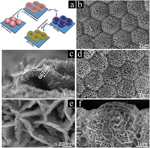
a) Scheme of the preparation processes of SnO2/TiO2/BiVO4 H‐NSs@HMs arrays. SEM images of SnO2 H‐NSs@HMs arrays: b) top view and c) cross‐section view. SnO2/TiO2/BiVO4 H‐NSs@HMs arrays: d,e) top view and f) cross‐section view.
Figure 1b shows top view of the SnO2 H‐NSs@HMs arrays. It can be seen that a number of ultrathin SnO2 nanosheets are uniformly assembled on each hollow microsphere, forming a hierarchical hollow nanosheets@microspheres core–shell structure with diameters of ≈4.5 µm. Noting that the hierarchically hollow microspheres are periodically distributed on the substrate, which would be beneficial to the light harvesting and charge transport. From the cross‐section view in Figure 1c, it can be observed that the thickness of individual nanosheet is ranging from 5 to 30 nm, and the whole nanosheets layer thickness is ≈667 nm. After the deposition of TiO2 and BiVO4, the ordered structure is still well preserved, as displayed in Figure 1d, indicating the conformal thin films deposition by ALD and electrodeposition, respectively. From a closer observation in Figure 1e,f, the nanosheet surfaces become more rough after the deposition of BiVO4 and the nanosheet thickness increased obviously. The BiVO4 layer thickness can be determined to be ≈20 nm. It is noteworthy that the BiVO4 films are consisted of lots of large grains with diameters from 30 to 50 nm, which are advantageous for further improving the light absorption and increasing the specific surface area. The mapping results and energy dispersive X‐ray spectrum (EDX) in Figures S2 and S3 in the Supporting Information recorded from the SnO2/TiO2/BiVO4 H‐NSs@HMs prove the existence and uniform elements distributions of Sn, Ti, Bi, V, and O. For comparison, SnO2/TiO2/BiVO4 nanosheets arrays, SnO2/TiO2/BiVO4 hollow microspheres arrays, and SnO2/TiO2/BiVO4 hierarchical hollow nanosheets@microspheres arrays with different diameters are also prepared, the corresponding scanning electron microscopy (SEM) images are provided in Figures S4–S6 in the Supporting Information, respectively.
The transmission electron microscopy (TEM) image of the SnO2/TiO2 nanosheet in Figure 2 a confirms that TiO2 are uniformly covered on the SnO2 nanosheet, suggesting the uniform and conformal film deposition by ALD. It can be seen that the nanosheet is consisted of nanoparticles with lots of mesopores. The mesoporous structures would be beneficial to increase the interface area and facilitate the electrolyte infiltration. The measured spacing of 0.26 and 0.35 nm in Figure 2b can be assigned to tetragonal phase of SnO2 and anatase phase of TiO2, respectively. After the BiVO4 deposition, a number of nanoplates are uniformly distributed on the SnO2/TiO2 nanosheet, as shown in Figure 2c, which is in agreement of the SEM observations. The lattice spacings of 0.47, 0.29, 0.26, and 0.35 nm in Figure 2d correspond to the (110), (040) planes of monoclinic BiVO4, (101) planes of tetragonal SnO2, and (101) planes of anatase TiO2, respectively.
Figure 2.
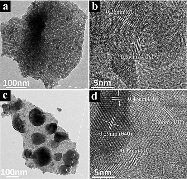
TEM image and high‐resolution TEM images of a,b) SnO2/TiO2 H‐NSs@HMs arrays and c,d) SnO2/TiO2/BiVO4 H‐NSs@HMs arrays.
The crystal structure of SnO2 H‐NSs@HMs and SnO2/TiO2/BiVO4 H‐NSs@HMs were analyzed by X‐ray diffraction (XRD). As displayed in Figure 3 a, the peaks of 26.41°, 34.06°, 37.88°, 51.67°, 61.87°, and 65.94° correspond to (110), (101), (200), (211), (310), and (301) planes of tetragonal phase of SnO2 (Joint Committee on Powder Diffraction Standards (JCPDS) No. 41‐1445), while the other peaks can be assigned to monoclinic BiVO4 phase (JCPDS No. 14‐0688). The chemical composition and surface states of SnO2/TiO2/BiVO4 H‐NSs@HMs was characterized by X‐ray photoelectron spectrum (XPS). The full survey spectrum in Figure S7 in the Supporting Information records the V, Sn, Ti, Bi, and O elements. The high‐resolution Sn element XPS spectra in Figure 3b show two peaks at 486.7 and 495.1 eV respectively, corresponding to Sn4+ in SnO2. The two satellite peaks of the high‐resolution Ti 2p3/2 and Ti 2p1/2 in Figure 3c centered at binding energies 458.5 and 464.6 eV are typical characteristic Ti4+ binding in TiO2. The signal at Ti 2p1/2 is asymmetric and has shoulders on the lower energy side, which might be related to the combination of BiVO4 and SnO2.46, 47, 48 The high‐resolution Bi, V, and O spectra can help identify the built‐in potential in the interface. The binding energy located at 159.1 and 164.5 eV in Figure 3d correspond to the Bi 4f7/2 orbit and Bi 4f5/2 orbit, respectively. The splitting peaks at 512.0 and 516.7 eV in Figure 3e correspond to V 2p3/2 orbit and V 2p1/2 orbit, respectively.49, 50, 51, 52 The high‐resolution O 1s XPS spectra in Figure 3f show two peaks, one has the binding energy at 530.0 eV is attributed to the lattice oxygen of the Sn—O, Ti—O, Bi—O, and V—O, and the other peak at 532.0 eV can be assigned to the hydroxide in O—H and adsorbed oxygen.53, 54 The high‐resolution Fe 2p spectra and Ni 2p spectra results in Figure S8 in the Supporting Information indicated that FeOOH/NiOOH catalyst were successfully deposited on the SnO2/TiO2/BiVO4 hierarchical structures.24
Figure 3.
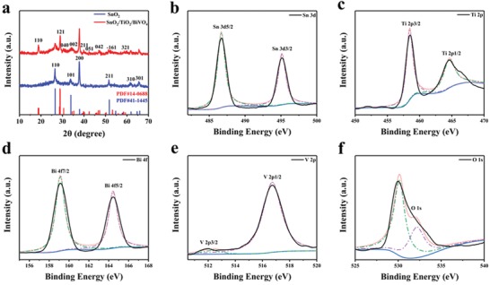
a) X‐ray diffraction (XRD) pattern of SnO2 and SnO2/TiO2/BiVO4 H‐NSs@HMs arrays. XPS core elemental spectrum recorded from SnO2/TiO2/BiVO4 H‐NSs@HMs: b) Sn 3d, c) Ti 2p, d) Bi 4f, e) V 2p, and f) O 1s.
The light absorption characteristics of as fabricated samples are characterized by diffuse reflectance spectrum and transmittance spectrum. Figure 4 a shows the diffuse reflectance spectrum of SnO2, SnO2/TiO2, SnO2/TiO2/BiVO4, and SnO2/BiVO4 H‐NSs@HMs arrays. For the SnO2 and SnO2/TiO2 H‐NSs@HMs arrays, the observed absorption edges of ≈310 and ≈350 nm are corresponding to the bandgap of SnO2 and TiO2, respectively. After the deposition of BiVO4, the absorption edge redshifts to ≈450 nm, which is in agreement of the bandgap absorption of BiVO4. It is worth noting that the SnO2/TiO2/BiVO4 H‐NSs@HMs arrays display the lowest light reflectance and light transmittance intensity in the measured wavelength of 300–700 nm among all the referenced samples, as shown in Figure 4a and Figure S9 in the Supporting Information, indicating that the SnO2/TiO2/BiVO4 H‐NSs@HMs arrays possess the highest light capturing ability, due to the ordered hierarchy structure as well as synergistic effect between each component in the composite. To demonstrate the omnidirectional light harvesting ability of the SnO2/TiO2/BiVO4 H‐NSs@HMs arrays, the specular reflection spectra at different light incidence angles are measured. As shown in Figure 4b, the SnO2/TiO2/BiVO4 H‐NSs@HMs arrays exhibits excellent omnidirectional antireflection characteristics with light reflection intensity below 1% in a wide wavelength range of 300 to 1100 nm. The excellent omnidirectional light harvesting ability could be due to the periodically ordered hierarchy structures that result in multiple light scattering, increased optical paths, and reduced light reflectance.29, 55
Figure 4.
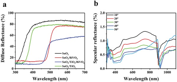
a) UV–vis diffuse reflectance spectra of SnO2, SnO2/TiO2, SnO2/BiVO4, SnO2/TiO2/BiVO4 H‐NSs@HMs arrays. b) Specular reflectance spectra of SnO2/TiO2/BiVO4 H‐NSs@HMs arrays at incident angles of 10°, 20°, 30°, 40°, and 50°.
The PEC performance of as‐fabricated samples is evaluated by linear sweep voltammetric (LSV) measurement under AM1.5 simulated light illumination (100 mW cm−2). The measurement was conducted in 0.5 m Na2SO4 electrolyte with 0.1 m Na2SO3 as a hole scavenger due to the fast kinetics of the sulfite oxidation. Figure 5 a shows the comparison LSV curves of three electrodes with different morphology measured in the dark and light conditions of SnO2/TiO2/BiVO4 hollow microspheres (HMs) arrays, SnO2/TiO2/BiVO4 nanosheets (NSs) arrays, and SnO2/TiO2/BiVO4 H‐NSs@HMs arrays. It can be seen that all the electrodes exhibit negligible photocurrent density under dark condition. While under light illumination, obvious photocurrent density is observed. The SnO2/TiO2/BiVO4 H‐NSs@HMs arrays photoanode shows the highest PEC performance with a maximum photocurrent density of 5.03 mA.cm−2 at 1.23 V versus RHE, which is much higher than that of SnO2/TiO2/BiVO4 hollow microspheres arrays and SnO2/TiO2/BiVO4 nanosheets arrays. Our results are superior to most of the recent reports on BiVO4 based photoanodes, as listed in Table S1 in the Supporting Information. The significantly improved PEC performance could be due to the hierarchically ordered structure that provides large specific surface area and efficient interface contact, resulting in improved light absorption and charge separation efficiency. To further illustrate the important role of TiO2 layer on the PEC performance, SnO2/TiO2/BiVO4 H‐NSs@HMs samples with different TiO2 layer thickness were prepared. As shown in Figure 5b, all the SnO2/TiO2/BiVO4 H‐NSs@HMs arrays photoanodes exhibit much better PEC performance in contrast to that of SnO2/BiVO4 H‐NSs@HMs arrays. The greatly improved performance might be due to the important role of TiO2 acting as a hole blocking layer to improve the charge separation efficiency and reduce the recombination rates. Noting that the optimized TiO2 layer thickness is ≈5 nm because a thicker TiO2 layer would affect the charge transport and reduce the PEC performance. Moreover, the effect of microspheres sizes and BiVO4 layer thickness on the PEC performance of SnO2/TiO2/BiVO4 H‐NSs@HMs arrays photoanode was also investigated. As shown in Figure S10 in the Supporting Information, the SnO2/TiO2/BiVO4 H‐NSs@HMs arrays electrode with diameters of ≈4.5 µm and moderate BiVO4 layer thickness display the optimized performance. Figure 5c shows the LSV curves measured under light on/off cycles, all the photoanodes show fast photoresponse and recovery time. The photoelectrochemical sulfite oxidation efficiency can be expressed as Equation (1)
| (1) |
where J sulftie is defined as the photocurrent density of sulfite oxidation, J max is defined the maximum photocurrent density, ηabs is the light absorption efficiency, ηsep is the charge separation efficiency, and ηtran s is the charge transfer efficiency. Assuming that ηtrans is ≈100% at 1.23 V versus RHE in the presence of hole scavengers, the ηabs × ηsep = J sulftie/J max. In our system, the J max is calculated to be ≈6.67 mA.cm−2 by using photon energy and solar photon flux at 300–515 nm,14, 56 the calculation details are provided in the Supporting information. The ηabs is determined by the light harvesting efficiency (LHE), i.e., LHE (%) = 100% − R(λ) (%) − T(λ) (%), as plotted in Figure 5d. Hence, the ηsep can be determined. As shown in Figure 5e, the SnO2/TiO2/BiVO4 H‐NSs@HMs arrays electrode shows the highest charge separation efficiency of 84.9% in contrast to that of SnO2/BiVO4 H‐NSs@HMs arrays, SnO2/TiO2/BiVO4 HMs arrays and SnO2/TiO2/BiVO4 NSs arrays. Moreover, the PEC water splitting performance SnO2/TiO2/BiVO4 H‐NSs@HMs arrays with and without FeOOH/NiOOH catalyst were measured in 0.5 m Na2SO4 electrolyte. As shown in Figure 5f, the FeOOH/NiOOH‐modified SnO2/TiO2/BiVO4 H‐NSs@HMs arrays photoanode shows significantly enhanced performance, yielding a maximum photocurrent density value of ≈3.1 mA cm−2 at 1.23 V versus RHE. This might be due to the role of the FeOOH and NiOOH dual water oxidation catalyst, which could facilitate the hole transfer efficiency and improve the water oxidation kinetics.
Figure 5.
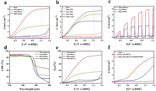
LSV curves measured under simulated light and dark conditions in 0.5 m Na2SO4 solution with 0.1 m Na2SO3 a) SnO2/TiO2/BiVO4 HMs, SnO2/TiO2/BiVO4 NSs, and SnO2/TiO2/BiVO4 H‐NSs@HMs arrays. b) Comparison of SnO2/TiO2/BiVO4 H‐NSs@HMs arrays with different TiO2 layer thickness. c) Chopped photocurrent‐potential curves of SnO2/TiO2/BiVO4 HMs, SnO2/TiO2/BiVO4 NSs, and SnO2/TiO2/BiVO4 H‐NSs@HMs arrays. d,e) Light harvesting efficiency (LHE) and charge separation efficiency (ηsep) of SnO2/TiO2/BiVO4 HMs, SnO2/TiO2/BiVO4 NSs, SnO2/BiVO4 H‐NSs@HMs arrays, and SnO2/TiO2/BiVO4 H‐NSs@HMs arrays. f) PEC water splitting performance of SnO2/TiO2/BiVO4 H‐NSs@HMs arrays with and without FeOOH/NiOOH water oxidation catalyst.
In order to study the wavelength‐dependent photoactivity of as‐fabricated photoanodes, the incident photoelectric conversion efficiency (IPCE) tests were conducted in a three‐electrode system at 1.23 V versus RHE. The IPCE can be calculated by the following formula (2)
| (2) |
where I is the photocurrent density, λ is the wavelength of the incident light, and J light represents the incident light power intensity. As displayed in Figure 6 a, the SnO2/TiO2/BiVO4 H‐NSs@HMs arrays electrode displays the highest IPCE values in the wavelength of 325–475 nm in contrast to that of the other two reference samples and a maximum IPCE value of ≈85% was reached at 350 nm. The improved IPCE results of SnO2/TiO2/BiVO4 H‐NSs@HMs arrays could be due to its high light absorption and charge separation efficiency.57, 58, 59 To exclude the light absorption effect in the three different electrodes, the absorption photoelectric conversion efficiency (APCE) is used to determine quantum efficiency based on the IPCE and UV–vis absorption spectra results.31 As shown in Figure 6b, the SnO2/TiO2/BiVO4 H‐NSs@HMs also yield the highest APCE efficiency in the wavelength range of 300–500 nm. This would be attributed to the ordered structure that provides large interface contact area, facilitating the charge transport, separation, and collection process.
Figure 6.
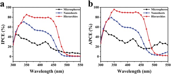
a) IPCE spectra and b) spectra APCE of SnO2/TiO2/BiVO4 hollow microspheres arrays, SnO2/TiO2/BiVO4 nanosheets arrays and SnO2/TiO2/BiVO4 H‐NSs@HMs arrays collected at 1.23 V versus RHE.
In order to understand the charge transfer process of SnO2/TiO2/BiVO4 electrodes, electrochemical impedance spectroscopy (EIS) measurements on the three different structures were conducted under open circuit with AM1.5 simulated light illumination. As shown in the EIS spectra in Figure 7 a, the semicircle radius in the middle frequency range represents the charge transfer resistance at the photoelectrode/electrolyte interface, the SnO2/TiO2/BiVO4 H‐NSs@HMs photoanode shows the lowest charge transfer resistance in comparison to the counterparts, suggesting that the hierarchically ordered electrode has improved charge transport and separation efficiency. Besides, the SnO2/TiO2/BiVO4 electrode shows lower charge transfer resistance in contrast to that of SnO2/TiO2 and SnO2/BiVO4 samples (as shown in Figure S12, Supporting Information), indicating that the TiO2 layer is beneficial to facilitate the charge transfer process.
Figure 7.
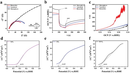
a) EIS spectra of SnO2/TiO2/BiVO4 hollow microspheres arrays, SnO2/TiO2/BiVO4 nanosheets arrays, and SnO2/TiO2/BiVO4 H‐NSs@HMs arrays measured under open circuit with light illumination. b,c) Open circuit voltage decay (OCVD) and electron lifetime of SnO2/TiO2/BiVO4 HMs, SnO2/TiO2/BiVO4 NSs, and SnO2/TiO2/BiVO4 H‐NSs@HMs arrays. Mott–Schottky plots measured in the dark at frequency of 500 Hz: d) SnO2, e) planar TiO2 films, and f) BiVO4 films.
The minority carrier lifetime (τ) is an important parameter affecting the overall conversion efficiency of semiconductor electrodes. The recombination kinetics of as‐fabricated SnO2/TiO2/BiVO4 samples were studied by open circuit voltage decay (OCVD) route, in which the photovoltage decay rate is directly related to the electron lifetime, and the lifetime of the injected electron can be obtained according to Equation (3), 60
| (3) |
where k B is the Boltzmann constant, T is the temperature, e is the electron charge, d Voc is the amount of change in photovoltage, and dt is the amount of change in time. The k B T/e is ≈0.026 V at room temperature. Therefore, the lifetime can be determined based on the OCVD curves in Figure 7c. As shown in Figure 7d, the SnO2/TiO2/BiVO4 H‐NSs@HMs arrays photoanode show prolonged carrier life time in comparison with the counterparts of SnO2/TiO2/BiVO4 HMs and SnO2/TiO2/BiVO4 NSs, resulting in the reduced recombination rates and improved charge separation efficiency. Moreover, the SnO2/TiO2/BiVO4 H‐NSs@HMs also have increased carrier life time in comparison to that of SnO2/TiO2 and SnO2/BiVO4 H‐NSs@HMs arrays, further indicating that the medium TiO2 layer can facilitate the charge separation and reduce the charge recombination, leading to enhanced PEC performance, as shown in Figure S13 in the Supporting Information.
The flat band potential (V fb) is measured by the open circuit potential of the photocurrent. The flat band potential V fb of SnO2, TiO2, and BiVO4 in the composite can be determined by the Mott–Schottky curve as Equation (4)
| (4) |
where C is the capacitance of the space charge layer, e is the electron charge, ε is the dielectric constant, ε0 is the dielectric constant of the vacuum, N d is the density of the electron donor, V a is the applied potential, V fb is the flat potential, K B is the Boltzmann constant, and T is temperature. The V fb is determined by a linear fit of the x intercept as function of 1/c2. As shown in Figure 7d–f, the V fb of SnO2, TiO2, and BiVO4 are determined to be 0.27, 0.14, and 0.12 V (vs RHE), respectively. Assuming that the gap between the conduction band bottom edge and V fb can be ignored, the difference in the V fb values confirms the feasible electron transfer from BiVO4 to TiO2.
To further determine the valence band positions, ultraviolet photoelectron spectroscopy (UPS) measurements on SnO2, TiO2, and BiVO4 were conducted. The valence band edges were calculated using the photon energy of He I (21.22 eV) and the low kinetic energy cutoff of the spectrum and the valence band maximum with respect to the Fermi level (E F).61 As shown in Figure S14a in the Supporting Information, the valence band positions of SnO2, TiO2, and BiVO4 are found to be 7.93, 7.58, and 6.93 eV versus the E vac or 3.49, 3.14, and 2.49 eV on the RHE.
The electronic transfer mechanism can be illustrated in Figure 8 . The band alignment was confirmed by the optical bandgap from the UV–vis absorption spectra (Figure S14b, Supporting Information) and the valence band edges measured by UPS. In the SnO2/TiO2/BiVO4 heterojunctions system, the TiO2/BiVO4 and TiO2/SnO2 build cascade structured band alignment, which significantly improve the charge separation and reduce the charge recombination at the interface.61, 62, 63 Under light excitation, both BiVO4 and TiO2 can absorb photons and generate electron–hole pairs. The photogenerated electrons in BiVO4 facilitated to transfer to the conduction band of TiO2 due to the type II configuration and then transported by the conductive SnO2 skeletons.64 The significantly enhanced PEC performance can be due to the following reasons. First, the hierarchically ordered hollow microspheres/nanosheets arrays structure can provide large specific area and rich porosity, as result in improved light harvesting efficiency. Second, the type II heterojunction and excellent contact between the TiO2 and BiVO4 facilitate the charge separation efficiency. Third, the enhanced charge injection and charge transfer process in the electrode/electrolyte interface of ordered SnO2/TiO2/BiVO4 also contribute the improved charge transport and separation. The last but not the least, the synergistic effect of each component in the ternary composite leads to the improved overall performance.
Figure 8.
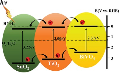
The electronic transfer mechanism of SnO2/TiO2/BiVO4 H‐NSs@HMs arrays.
3. Conclusions
In summary, we have designed and fabricated a 3D hierarchical ternary SnO2/TiO2/BiVO4 arrays photoanode for photoelectrochemical application. The unique hierarchically ordered electrode design and synergistic effect between each component in the SnO2/TiO2/BiVO4 photoanode led to improved charge transport efficiency, light harvesting efficiency, and charge separation efficiency, as a result in significantly improved PEC performance. Our results demonstrate that electrode design and interface engineering play important roles to boost the overall PEC performance and would open new opportunities for design of various heterojunction photoelectrodes for solar energy conversion.
4. Experimental Section
Preparation of SnO2/TiO2/BiVO4 Hierarchical Nanosheets@Hollow Microspheres (H‐NSs@HMs) Arrays: The preparation processes SnO2/TiO2/BiVO4 hierarchical nanosheets@hollow microspheres (H‐NSs@HMs) arrays can be divided into three steps. First, SnO2 H‐NSs@HMs arrays on FTO substrate were prepared by colloid spheres template, ALD, and hydrothermal growth process. Second, TiO2 films with different thicknesses were deposited on SnO2 H‐NSs@HMs by ALD. The sample was placed in the ALD apparatus, and TiCl4 and H2O were used as Ti and O source, respectively. The temperature was 80 °C and the pressure was 11 × 103 Pa. Finally, on layer of BiVO4 was deposited on the surface by electrochemical deposition route35 and the thickness was controlled by deposition times. For comparison, SnO2/TiO2/BiVO4 hollow microspheres array and SnO2/TiO2/BiVO4 nanosheets arrays are also prepared. The experiment details are described in the Supporting information.
Characterizations: The surface morphology of the samples was observed using field electron and ion company (FEI) Sirion 200 field emission SEM. The microstructure of the sample was characterized using JEM 2014F TEM. The phase analysis was carried out by XRD (D8‐Advance, Bruker Miller). The content of each component was determined by energy dispersive X‐ray Spectroscopy (EDX) of an X‐max 80 (Oxford) model. X‐ray photoelectron spectroscopy (Kratos Axis Ultra delay line detector (DLD)) characterizes elemental composition and valence state. Ultraviolet photoelectron spectroscopy measurements were conducted out on an ThermoFisher ESCALAB 250 XI spectrometer with a He discharge lamp (He I line, 21.22 eV) as the excitation source and a sample bias of −5 V was applied. The diffuse reflectance spectra were obtained on ultraviolet—see spectrophotometer (Hatachi, U3900H) and Specular reflectance spectra were recorded on Lambda 950 spectrophotometer.
PEC Measurements: The PEC performance of the samples was measured by electrochemical workstation (CS350, CS instrument) with simulated AM1.5G (100 mW cm−2) light illumination. The samples, Ag/AgCl (3M KCl), and Pt foil were employed as working electrodes, reference electrode, and counter electrode, respectively. The electrolyte was 0.5 m Na2SO4 mixed solution with 0.1 m Na2SO3 as hole scavenger. The measured potentials was converted from Ag/AgCl to the RHE by the following formula (5)
| (5) |
E RHE is the potential of the RHE, E Ag/AgCl is the potential of the reference electrode Ag/AgCl, and pH is the pH value of the electrolyte. Simulated sunlight with 100 mW cm−2 was offered by a solar simulator (Zolix SS150). EIS spectra were measured in the frequency range of 10−1 to 105 Hz under a 10 mV amplitude. IPCE values were obtained by IPCE system (Zolix Solar cell Scan100) in the wavelength range of 300–550 nm at the bias of 1.23 V versus RHE.
Conflict of Interest
The authors declare no conflict of interest.
Supporting information
Supporting Information
Acknowledgements
This work was financial support by the National Natural Science Foundation of China (Grant No. 51772213), Shanghai Science and Technology Committee (Grant Nos. 18ZR1442300 and 18JC1410900), and the Fundamental Research Funds for the Central Universities.
Pan Q., Li A. S., Zhang Y. L., Yang Y. P., Cheng C. W., Rational Design of 3D Hierarchical Ternary SnO2/TiO2/BiVO4 Arrays Photoanode toward Efficient Photoelectrochemical Performance. Adv. Sci. 2020, 7, 1902235 10.1002/advs.201902235
References
- 1. Boettcher S. W., Spurgeon J. M., Putnam M. C., Warren E. L., Turner‐Evans D. B., Kelzenberg M. D., Maiolo J. R., Atwater H. A., Lewis N. S., Science 2010, 327, 185. [DOI] [PubMed] [Google Scholar]
- 2. Shen S. H., Chen J., Wang M., Sheng X., Chen X. Y., Feng X. J., Mao S. S., Prog. Mater. Sci. 2018, 98, 299. [Google Scholar]
- 3. Prévot M. S., Sivula K., J. Phys. Chem. C 2013, 117, 17879. [Google Scholar]
- 4. Tountas A. A., Peng X. Y., Tavasoli A. V., Duchesne P. N., Dingle T. L., Dong Y. C., Hurtado L., Mohan A., Sun W., Ulmer U., Wang L., Wood T. E., Maravelias C. T., Sain M. M., Ozin G. A., Adv. Sci. 2019, 6, 1801903. [DOI] [PMC free article] [PubMed] [Google Scholar]
- 5. Freitas R. G., Santanna M. A., Pereira E. C., Electrochim. Acta 2014, 136, 404. [Google Scholar]
- 6. Li Y. Y., Wang J. H., Luo Z. J., Chen K., Cheng Z. Q., Ma L., Ding S. J., Zhou L., Wang Q. Q., Sci. Rep. 2017, 7, 7178. [DOI] [PMC free article] [PubMed] [Google Scholar]
- 7. Kment S., Riboni F., Pausova S., Wang L., Wang L. Y., Han H., Hubicka Z., Krysa J., Schmuki P., Zboril R., Chem. Soc. Rev. 2017, 46, 3716. [DOI] [PubMed] [Google Scholar]
- 8. She X. J., Wu J. J., Xu H., Zhong J., Wang Y., Song Y. H., Nie K. Q., Liu Y., Yang Y. C., Rodrigues M. F., Vajtai R., Lou J., Du D., Li H. M., Ajayan P. M., Adv. Energy Mater. 2017, 7, 1700025. [Google Scholar]
- 9. Liu S. X., Zheng L. X., Yu P. P., Han S. C., Fang X. S., Adv. Funct. Mater. 2016, 26, 3331. [Google Scholar]
- 10. Toma F. M., Cooper J. K., Kunzelmann V., McDowell M. T., Yu J., Larson D. M., Borys N. J., Abelyan C., Beeman J. W., Yu K. M., Yang J. H., Chen L., Shaner M. R., Spurgeon J., Houle F. A., Persson K. A., Sharp I. D., Nat. Commun. 2016, 7, 12012. [DOI] [PMC free article] [PubMed] [Google Scholar]
- 11. Eichhorn J., Kastl C., Cooper J. K., Ziegler D., Schwartzberg A. M., Sharp I. D., Toma F. M., Nat. Commun. 2018, 9, 2597. [DOI] [PMC free article] [PubMed] [Google Scholar]
- 12. Tan H. L., Amal R., Ng Y. H., J. Mater. Chem. A 2017, 5, 16498. [Google Scholar]
- 13. Liu G. J., Eichhorn J., Jiang C. M., Scott M. C., Hess L. H., Gregoire J. M., Haber J. A., Sharp I. D., Toma F. M., Sustainable Energy Fuels 2019, 3, 127. [Google Scholar]
- 14. Kim T. W., Choi K. S., Science 2014, 343, 990. [DOI] [PubMed] [Google Scholar]
- 15. Qiu Y. C., Liu W., Chen W., Zhou G. M., Hsu P. C., Zhang R. F., Liang Z., Fan S. S., Zhang Y. G., Cui Y., Sci. Adv. 2016, 2, e1501764. [DOI] [PMC free article] [PubMed] [Google Scholar]
- 16. Kim T. W., Ping Y., Galli G. A., Choi K. S., Nat. Commun. 2015, 6, 8769. [DOI] [PMC free article] [PubMed] [Google Scholar]
- 17. Zhou L., Zhao C. Q., Giri B., Allen P., Xu X. W., Joshi H., Fan Y. Y., Titova L. V., Rao P. M., Nano Lett. 2016, 16, 3463. [DOI] [PubMed] [Google Scholar]
- 18. Wang S. C., Chen P., Bai Y., Yun J. H., Liu G., Wang L. Z., Adv. Mater. 2018, 30, 1800486. [DOI] [PubMed] [Google Scholar]
- 19. Pasumarthi V., Liu T. F., Dupuis M., Li C., J. Mater. Chem. A 2019, 7, 3054. [Google Scholar]
- 20. Zhang K. F., Liu Y. X., Deng J. G., Xie S. H., Zhao X. T., Yang J., Han Z., Dai H. X., Appl. Catal., B 2018, 224, 350. [Google Scholar]
- 21. Patil S. S., Mali M. G., Hassan M. A., Patil D. R., Kolekar S. S., Ryu S. W., Sci. Rep. 2017, 7, 8404. [DOI] [PMC free article] [PubMed] [Google Scholar]
- 22. Li R. G., Zhang F. X., Wang D., Yang J. X., Li M. R., Zhu J., Zhou X., Han H. X., Li C., Nat. Commun. 2013, 4, 1432. [DOI] [PubMed] [Google Scholar]
- 23. Lee Y. W., Boonmongkolras P., Son E. J., Kim J., Lee S. H., Kuk S. K., Ko J. W., Shin B., Park C. B., Nat. Commun. 2018, 9, 4208. [DOI] [PMC free article] [PubMed] [Google Scholar]
- 24. Zhang K., Jin B. J., Park C., Cho Y., Song X. F., Shi X. J., Zhang S. L., Kim W., Zeng H. B., Park J. H., Nat. Commun. 2019, 10, 2001. [DOI] [PMC free article] [PubMed] [Google Scholar]
- 25. Liu C., Dasgupta N. P., Yang P. D., Chem. Mater. 2014, 26, 415. [Google Scholar]
- 26. Wu W. Q., Chen D. H., Cheng Y. B., Caruso R. A., Sol. RRL 2017, 1, 1700117. [Google Scholar]
- 27. Zhang H. F., Cheng C. W., ACS Energy Lett. 2017, 2, 813. [Google Scholar]
- 28. Zhang H. F., Zhang D., Qin X. M., Cheng C. W., J. Phys. Chem. C 2015, 119, 27875. [Google Scholar]
- 29. Ren W. N., Zhang H. F., Kong D. Z., Liu B., Yang Y. P., Cheng C. W., Phys. Chem. Chem. Phys. 2014, 16, 22953. [DOI] [PubMed] [Google Scholar]
- 30. Zheng L. X., Han S. C., Liu H., Yu P. P., Fang X. S., Small 2016, 12, 1527. [DOI] [PubMed] [Google Scholar]
- 31. Pan Q., Zhang H. F., Yang Y. P., Cheng C. W., Small 2019, 15, 1900924. [DOI] [PubMed] [Google Scholar]
- 32. Li X., Yu J. G., Low J. X., Fang Y. P., Xiao J., Chen X. B., J. Mater. Chem. A 2015, 3, 2485. [Google Scholar]
- 33. Pingmuang K., Chen J., Kangwansupamonkon W., Wallace G. G., Phanichphant S., Nattestad A., Sci. Rep. 2017, 7, 8929. [DOI] [PMC free article] [PubMed] [Google Scholar]
- 34. Resasco J., Zhang H., Kornienko N., Becknell N., Lee H., Guo J. H., Briseno A. L., Yang P. D., ACS Cent. Sci. 2016, 2, 80. [DOI] [PMC free article] [PubMed] [Google Scholar]
- 35. Xie M. Z., Fu X. D., Jing L. Q., Luan P., Feng Y. J., Fu H. G., Adv. Energy Mater. 2014, 4, 1300995. [Google Scholar]
- 36. Tian Z. L., Zhang P. F., Qin P., Sun D., Zhang S. N., Guo X. W., Zhao W., Zhao D. Y., Huang F. Q., Adv. Energy Mater. 2019, 9, 1901287. [Google Scholar]
- 37. Zhou Y. G., Zhang L. Y., Lin L. H., Wygant B. R., Liu Y., Zhu Y., Zheng Y. B., Mullins C. B., Zhao Y., Zhang X. H., Yu G. H., Nano Lett. 2017, 17, 8012. [DOI] [PubMed] [Google Scholar]
- 38. Ouyang W. X., Teng F., Fang X. S., Adv. Funct. Mater. 2018, 28, 1707178. [Google Scholar]
- 39. Zhang H. F., Zhou W. W., Yang Y. P., Cheng C. W., Small 2017, 13, 1603840. [Google Scholar]
- 40. Grigioni I., Stamplecoskie K. G., Selli E., Kamat P. V., J. Phys. Chem. C 2015, 119, 20792. [Google Scholar]
- 41. Grigioni I., Stamplecoskie K. G., Jara D. H., Dozzi M. V., Oriana A., Cerullo G., Kamat P. V., Selli E., ACS Energy Lett. 2017, 2, 1362. [Google Scholar]
- 42. Shi1 X. J., Jeong H., Oh S. J., Ma M., Zhang K., Kwon J., Choi I. T., Choi I. Y., Kim H. K., Kim J. K., Park J. H., Nat. Commun. 2016, 7, 11943. [DOI] [PMC free article] [PubMed] [Google Scholar]
- 43. Bera S., Lee S. A., Kim C. M., Khan H., Jang H. W., Kwon S. H., Chem. Mater. 2018, 30, 8501. [Google Scholar]
- 44. Chen S. Y., Yang J. S., Wu J. J., ACS Appl. Energy Mater. 2018, 1, 2143. [Google Scholar]
- 45. Kim J. H., Jang J. W., Jo Y. H., Abdi F. F., Lee Y. H., Krol R. V., Lee J. S., Nat. Commun. 2016, 7, 13380. [DOI] [PMC free article] [PubMed] [Google Scholar]
- 46. Zhang X., Liu Y., Lee S. T., Yang S., Kang Z. H., Energy Environ. Sci. 2014, 7, 1409. [Google Scholar]
- 47. Wang G. M., Wang H. Y., Ling Y. C., Tang Y. C., Yang X. Y., Fitzmorris R. C., Wang C. C., Zhang J. Z., Li Y., Nano Lett. 2011, 11, 3026. [DOI] [PubMed] [Google Scholar]
- 48. Chen X. B., Liu L., Yu P. Y., Mao S. S., Science 2011, 331, 746. [DOI] [PubMed] [Google Scholar]
- 49. Zhang L., Lin C. Y., Valev V. K., Reisner E., Steiner U., Baumberg J. J., Small 2014, 10, 3970. [DOI] [PMC free article] [PubMed] [Google Scholar]
- 50. Trześniewski B. J., Digdaya I. A., Nagaki T., Ravishankar S., Cardona I. H., Vermaas D. A., Longo A., Gimenezb S., Smith W. A., Energy Environ. Sci. 2017, 10, 1517. [Google Scholar]
- 51. Trześniewski B. J., Smith W. A., J. Mater. Chem. A 2016, 4, 2919. [Google Scholar]
- 52. Crist B. V., Handbook of Monochromatic XPS Spectra, Wiley‐VCH; 1999. [Google Scholar]
- 53. Cooper J. K., Gul S., Toma F. M., Chen L., Glans P. A., Guo J. H., Ager J. W., Yano J., Sharp I. D., Chem. Mater. 2014, 26, 5365. [Google Scholar]
- 54. Zhou M., Bao J., Xu Y., Zhang J. J., Xie J. F., Guan M. L., Wang C. L., Wen L. Y., Lei Y., Xie Y., ACS Nano 2014, 8, 7088. [DOI] [PubMed] [Google Scholar]
- 55. Cho I. S., Chen Z., Forman A. J., Kim D. R., Rao P. M., Jaramillo T. F., Zheng X. L., Nano Lett. 2011, 11, 4978. [DOI] [PubMed] [Google Scholar]
- 56.ASTM Standard G173‐03, 2008, Standard Tables for Reference Solar Spectral Irradiances: Direct Normal and Hemispherical on 37° Tilted Surface, ASTM International, West Conshohocken, PA 2003.
- 57. Ren H. J., Dittrich T., Ma H. Y., Hart J. N., Fengler S., Chen S., Li Y. B., Wang Y., Cao F. Y., Schieda M., Ng Y. H., Xie Z. R., Bo X., Koshy P., Sheppard L. R., Zhao C., Sorrell C. C., Adv. Mater. 2019, 31, 1807204. [DOI] [PubMed] [Google Scholar]
- 58. Kim J. K., Shi X. J., Jeong M. J., Park J., Han H. S., Kim S. H., Guo Y., Heinz T. F., Fan S. H., Lee C. L., Park J. H., Zheng X. L., Adv. Energy Mater. 2018, 8, 1701765. [Google Scholar]
- 59. Ma M., Kim J. K., Zhang K., Shi X., Kim S. J., Moon J. H., Park J. H., Chem. Mater. 2014, 26, 5592. [Google Scholar]
- 60. Xie Z., Liu X. X., Wang W. P., Wang X. J., Liu C., Xie Q., Li Z. C., Zhang Z. J., Nano Energy 2015, 11, 400. [Google Scholar]
- 61. Liu J., Liu Y., Liu N. Y., Han Y. Z., Zhang X., Huang H., Lifshitz Y., Lee S. T., Science 2015, 347, 970. [DOI] [PubMed] [Google Scholar]
- 62. Wu H. L., Li X. B., Tung C. H., Wu L. Z., Adv. Sci. 2018, 5, 1700684. [DOI] [PMC free article] [PubMed] [Google Scholar]
- 63. Singh A. P., Kodan N. S., Mehta B. R., Held A., Mayrhofer L., ACS Catal. 2016, 6, 5311. [Google Scholar]
- 64. Shen S. H., Lindley S. A., Dong C. L., Chen E. F., Lu Y. R., Zhou J. G., H Y. F., Wheeler D. A., Guo P. H., Zhang J. Z., Kliger D. S., Mao S. S., Sol. RRL 2018, 3, 1800285. [Google Scholar]
Associated Data
This section collects any data citations, data availability statements, or supplementary materials included in this article.
Supplementary Materials
Supporting Information


