

Abstract
Recently, the development of pressure sensor devices composed of mechanically flexible materials has gained a tremendous attention for emerging wearable electronics applications. Compared with various sensing materials, piezoelectric composite materials provide a characteristic advantage of enabling energy unit-free integration of sensor compartments. In this study, we develop a new chemical method of synthesizing highly functioning piezoelectric composite materials with electrostatically reinforced heterogeneous interfaces to improve the voltage output signal in all-printed sensor arrays. The surfaces of piezoelectric oxide nanoparticles are decorated subsequently with a cationic polyelectrolyte, polyethyleneimine, and a tri-block copolymer, styrene–ethylene/butylene–styrene grafted with maleic anhydride. To elucidate the factors determining the performance of pressure sensor devices, both the electrical properties and piezoelectric characteristics are investigated comprehensively for various compositional composite materials prepared from chemical and physical rubbers. The resulting device exhibits a sensitivity of 0.28 V·kPa–1 with a linear increment of output voltage in a pressure range up to 30 kPa. It is also demonstrated that the all-printed sensor array is fabricated successfully by a multistack-printing process of conductive, insulating, and piezoelectric composite materials in an additive manufacturing fashion.
1. Introduction
Deformable pressure sensors comprising flexible functional constituent materials can collect physical signals and quantify electrical signals from human activities.1,2 By virtue of their versatile potential for application in personal electronic devices and monitoring systems, flexible pressure sensors have received tremendous attention regarding their application in various wearable platform technologies, including human–machine interfaces, soft robotics, e-skin, and medical diagnosis.3−7 Conventional pressure sensors, composed of stiff materials, are generally unsuitable for such future applications. Pressure levels measurable in sensor devices can be categorized into four regimes, namely, ultra-low pressure, subtle pressure, low pressure, and medium pressure.1,8 Low pressure, ranging from a single-digit kilopascal to a few tens of kilopascals, is of particular importance in the monitoring of human activities and healthcare in daily life. The development of self-powered sensor systems is another prerequisite for solving the power consumption issue in various upcoming integrated systems.
To date, poly(vinylidene fluoride) (PVDF) derivatives have been incorporated as a flexible piezoelectric layer, owing to their easy capability of being casted in the form of thin film.9−12 However, their sensor performance is limited to some extent in comparison with inorganic piezoelectric materials, and PVDFs are difficult to be formulated into the inks that are suitable for various coating/printing techniques because of their limited solubility even in good solvents. The inorganic piezoelectric materials that exhibit excellent piezoelectric performance suffer from inherent mechanical brittleness. Recent efforts have been made to form flexible composite materials consisting of inorganic nanoparticles (NPs) and elastomers to resolve these issues.13−18 This colloidal approach is also advantageous in formulating the fluids applicable to specific printing techniques, as their rheological properties can be manifested, depending on the solid content in a polymer-incorporated suspension.
The practical potential of flexible piezoelectric composite materials has been demonstrated with recent developments of high-performance piezoelectric energy harvesters;19,20 however, highly functioning pressure sensor devices, employing piezoelectric composite materials, have been limitedly reported. In order for improving the sensor device performance, the strategies for forming spatially confined domain structures21,22 and adjusting a spatial arrangement of inorganic filler particles23 have been suggested in piezoelectric composite materials. However, excellent device performance was reported with an ultra-thin pure inorganic layer that can be flexible without imposing a high level of strain, exhibiting a sensitivity of 0.018 V·kPa–1 and a detectable range (in a linear trend) of 30 kPa.24 A common way of synthesizing composite materials for pressure sensor devices is simply mixing inorganic piezoelectric NPs with the poly(dimethylsiloxane) (PDMS), which is widely used in various stretchable applications, as an elastomer.14−16,19,20 To date, a study of establishing chemically reinforced heterogeneous interfaces between NPs and elastomers has been hardly reported, even with its importance in effectively delivering the stress provided from outer surroundings into piezoelectric inclusions. More importantly, even if the composite-based fluid is easily accessible to mask-free, inexpensive, large-area processable printing processes, most studies have not suggested a strategy for generating a position-addressable sensor array.
In this study, we have developed a new method of directly printing a high-performance piezoelectric pressure sensor array on a flexible substrate. A composite material is designed to have chemically reinforced interfaces between piezoelectric filler NPs and thermoplastic tri-block copolymers as an elastomer. This strengthened interaction between both compartments in composites allows for a uniform dispersion of inorganic NPs with much higher density as well as an efficient stress transfer to piezoelectric inorganic fillers with a number of junction interfaces. The multistacked array device is fabricated by the sequential printing process of piezoelectric, conductive, and insulating composite materials, using a 3-axis programmable dispensing machine without the involvement of any additional deposition/patterning processes. The fabricated device shows a sensitivity of 0.28 V·kPa–1 in a pressure range of 1–30 kPa.
2. Results and Discussion
2.1. Basic Electrical Properties of Various Elastomeric Polymers
Scheme 1 shows the procedure of formulating multistack printable composite pastes and fabricating the sensor devices. We investigated the piezoelectric composite materials comprising the lead zirconate titanate (PZT) NPs and various elastomeric polymers (EPs). The PZT NPs endow a pressure-sensitive piezoelectric property to composite materials, and the EPs provide mechanical flexibility to overcome a drawback of piezoelectric ceramics. The phase purity and morphology of the PZT NPs are shown in Figure S1. The pristine PZT NPs were mixed with EPs, PDMS, or thermoplastic tri-block copolymers of styrene–isoprene–styrene (SIS), styrene–ethylene/butylene–styrene (SEBS), and SEBS grafted with maleic anhydride (SEBSm). For PDMS, the ratio of prepolymer to curing agent was varied with values of 10:1, 20:1, and 30:1. To induce chemically reinforced heterogeneous interfaces between PZT NPs and EPs, we synthesized electrostatically functionalized PZT particles using polyethylenimine (PEI) and SEBSm. The chemically designed SEBSm–PEI-PZT NPs were mixed with a mixture of SEBS and SEBSm. For a highly conductive conductor paste, Ag flakes were mixed with PDMS and either 1,3-dichlorobenzene (DCB) or terpineol as a solvent. The basic properties of the composite materials were evaluated with all solution-processed bar-coated devices. Then, all-printed arrays were fabricated using a mask-free, three-axis programmable dispensing machine.
Scheme 1. Schematic of the Fabrication Procedures of the Bar-Coated Device and Multistack-Printed Array Device.

First, we evaluated the leakage current level for various EP-based metal–insulator–metal (MIM) devices to clarify whether they could withstand the high electric field applied during the poling process. Figure 1a shows the current densities at 2 MV/cm for the PDMS, SEBSm, SEBS, and SIS elastomers. For the PDMS and SEBSm elastomers, the low current densities were measured of ∼10–12 and 10–9 A/cm2 at 2 MV/cm, respectively; however, both SEBS and SIS elastomers do not block the currents penetrating through them even at low electric fields (Figure S2). At the electric field of 0.06 MV/cm, applied during the poling process in this study, the low leakage densities were measured of 3.6 × 10⁻¹¹ and 2.8 × 10⁻⁹ A/cm2 for the PDMS and SEBSm elastomers, respectively (Figure S3). The PDMS is a kind of chemical rubber that does not possess a partial-melt soft segment; it tends to be used as an insulating layer in the thin-film transistor (TFT) architecture.25,26 In thermoplastic physical rubbers, a soft segment with extremely low glass transition temperature is indispensable for endowing a stretchable property to polymeric structures.27,28 Interestingly, even if tri-block copolymer EPs of SIS, SEBS, and SEBSm have a similar chain structure, including polystyrene as a hard block segment, their leakage current behaviors vary widely depending on the nature of the soft block segment. The polystyrene is also another common insulating polymer used as a highly functioning dielectric in TFT.29,30 Thus, the leakage current behavior observable in SIS, SEBS, and SEBSm films may be determined by the chemical/physical nature of the soft block segment, which can be partly evaluated with the glass transition temperature (Tg). However, as seen in Figure 1b, there is no significant difference in Tg for all tri-block copolymer EPs, in comparison with that, 100 °C, for polystyrene. The values of Tg were measured to be −58.4, −53.6, and −52.9 °C for SIS, SEBS, and SEBSm films, respectively.
Figure 1.

(a) Current densities at an electric field of 2 MV/cm for MIM devices employing PDMS, SEBSm, SEBS, and SIS insulator layers; (b) glass transition temperatures and (c) stress–strain curves for PDMS, SEBSm, SEBS, and SIS films; (d) variations in the voltage signal as a function of pressure level in pPDMS and pSEBSm devices.
Variation in the compositional amount of the soft block segment can be another determining factor. This is directly related to how easily an elastomer is stretched under a given stress condition, which is represented by the elastic modulus. As seen in Figure 1c, the elastic moduli of the SIS, SEBS, and SEBSm films were measured to be 2, 11, and 20 MPa, respectively. This trend corresponds well to the leakage current results. Thus, we hypothesize that for the SEBSm layer, the compositional amount of soft segment is low enough to block the leakage current, whereas the SIS layer has an excessive amount of soft segment and in turn, does not show a proper insulating property. In particular, for the SIS-based MIM device, the upper Ag electrode was vacuum-deposited because of such a softness in the film structure; when the Ag composite electrode was cured at temperatures over 120 °C, the SIS films did not maintain their morphology. Note that, the PDMS film, a chemical rubber, has a quite low value of 0.8 MPa in elastic modulus, although it exhibits extreme insulating behavior. In this regard, to date, most piezoelectric composite materials have been studied with the use of PDMS rather than tri-block copolymer EPs with compositional variation.
2.2. Bar-Coated Sensor Devices Employing Pristine Piezoelectric NPs
The bar-coated devices employing PDMS, SIS, SEBS, and SEBSm-based pristine PZT composite layers are denoted as pPDMS, pSIS, pSEBS, and pSEBSm devices, respectively. As expected, for the pPDMS and pSEBSm devices, a poling voltage of 1 kV could be applied without any degradation of the electrical property. A low poling voltage of 10 V was applied to the pSEBS device, and the pSIS device was electrically short even at a voltage of 1 V (Figure S4). Figure 1d shows the voltage output as a function of pressure level in the pPDMS and pSEBSm devices. The recorded real data are shown in Figure S5. For both devices, the voltage output was measured with a value approaching merely to 0.3 V and was saturated at a pressure level as low as 5 kPa. The matrix polymer plays a critical role of transferring the stress imposed by outer surroundings as well as providing mechanical flexibility to the composite material. These factors would be affected by the elastic modulus of the matrix polymer. However, as seen in Figure S6, in the pPDMS devices prepared from the PDMS EPs with different elastic moduli, the voltage output characteristics did not vary significantly. This implies that a loss in imposing the stress at heterojunctions between piezoelectric NPs and polymers is much more critical than the aforementioned parameters.
2.3. Bar-Coated Sensor Devices Employing Electrostatically Functionalized Piezoelectric NPs
We designed the surface-functionalized piezoelectric NPs comprising the subsequent PEI and SEBSm layers (Figure 2a). The hydroxyl-terminated surface of oxide particles is protonated in the acidic aqueous medium with the generation of positively charged one, −OH2+, and deprotonated in the basic aqueous medium with a generation of negatively charged one, −O–.31 For the PZT NPs used in this study, the surface zeta potential values were measured to be 36.2, −6.9, −22.5, and −37.5 mV at the pH values of 2, 7, 10, and 12, respectively (Figure 2b). The PEI, a cationic polyelectrolyte with an amine-abundant chemical structure, tends to maintain its positive zeta potential even under a highly basic pH condition.32 By simply mixing the pristine PZT NPs and PEIs in an aqueous medium with the pH of 10, the positively charged PEI polymers bind electrostatically to the surface of negatively charged PZT particles. This is confirmed by the fact that the zeta potential of PEI-treated PZT NPs changed to the positive value of 25.3 mV at the pH of 10 (Figure 2b).
Figure 2.

(a) Schematic of showing the electrostatically functionalized SEBSm–PEI-PZT NPs. (b) Variation in zeta potential as a function of pH for pristine and PEI-PZT NPs and (c) photographs showing the dispersion stability in water and dichlorobenzene for pristine and SEBSm–PEI-PZT NPs. (d) FT-IR spectra for pristine PZT, PEI-PZT, and SEBSm–PEI-PZT NPs. The arrows represent the major chemical groups described in the manuscript. The chemical reaction between the amine group in PEI and the maleic anhydride in SEBSm is shown below the figure. (e) TEM image and compositional mapping data for SEBSm–PEI-PZT NPs.
The SEBSm polymer comprising maleic anhydride groups can undergo a vigorous chemical reaction with the amine group. Thus, electrostatically assembled SEBSm–PEI-PZT NPs are easily obtainable with a facile, simple mixing procedure at room temperature in air. As seen in Figure 2c, the hydroxyl-terminated pristine PZT and PEI-PZT NPs are dispersed well in water, while the SEBSm–PEI-PZT NPs are dispersed in 1,3-dichlorobezene, owing to the polar nature of PEI polymer and the nonpolar nature of SEBSm polymer. The multilayered surface functionalization was also confirmed by Fourier-transform infrared spectroscopy (FT-IR) spectral analysis (Figure 2d). Both pristine PZT and PEI-PZT NPs have a shoulder peak because of the stretch mode of O–H bonds at a wavenumber around 3000–3500 cm–1, commonly observable in polar surfaces. In the spectrum for PEI-PZT NPs, a characteristic peak at 1600 cm–1 is observed because of the bend mode of N–H bonds in the amine groups. In the spectrum for SEBSm–PEI-PZT NPs, the shoulder peak at 3000–3500 cm–1 vanished, with an evolution of the C–N stretch peaks in amide bonds at 950–1250 cm–1 and in aromatic amine at 1250–1330 cm–1.33 Uniform surface functionalization was confirmed by high-resolution transmission electron microscopy (TEM) imaging and the compositional mapping data for the SEBSm–PEI-PZT NPs (Figure 2e). The SEBSm–PEI-PZT NPs were well-dispersed in tri-block copolymer matrices, owing to excellent chemical compatibility, as seen in Figure S7. As seen in the cross-sectional scanning electron microscopy (SEM) image (Figure S8), no morphological defects were observable even after tearing the film in a liquid nitrogen bath.
We fabricated bar-coated sensor devices using the SEBSm–PEI-PZT NPs instead of pristine PZT NPs. The bar-coated device prepared from the piezoelectric composite layer employing the SEBSm–PEI-PZT NPs and a mixture of SEBS and SEBSm is referred to as the fSEBS/SEBSm device in this study. When the ratio by weight of SEBS to SEBSm is 7:3, that is described as the fSEBS(7)/SEBSm(3) device. Unexpectedly, the fSEBS(0)/SEBSm(10) device suffered from a low reproducibility because of a leakage current problem. SEBSm itself is a highly insulating polymer, as seen in Figure 1a,b; thus, this poor insulating property is attributable to the presence of a number of polar groups inside the composite layers. When both PEI and SEBSm polymers are reacted with the surface −O– groups of pristine PZT NPs and the amine groups of PEIs, respectively, they would experience a steric hindrance effect, leaving behind the unreacted OH groups (at neutral pH) and amine groups. It is well-known that these polar groups act as trap/de-trap sites where electrons can hop through them.34 The thermoplastic tri-block SEBSm polymer can wet the surface of NPs during drying at elevated temperature, encapsulating such polar groups. However, the softness of SEBSm polymer is not sufficient to cover them completely compared with those of SIS and SEBS EPs.
To encapsulate them more effectively, we used a mixture of SEBS and SEBSm as an elastomeric matrix. As seen in Figure 3a, with increasing the composition of SEBS up to 70 wt %, the output voltage as a function of pressure level was improved significantly, which may be attributed to the restricted loss of electric field in the fSEBS/SEBSm device. However, when the composition of SEBS increased to 90 wt %, the device performance deteriorated because of excessive incorporation of leaky SEBS polymer. The voltage outputs at 10 and 30 kPa are summarized in Figure 3b for all fSEBS/SEBSm devices. The fSEBS(7)/SEBSm(3) device exhibited the best performance with the output voltage of 0.8 V at a pressure of 30 kPa and the sensitivity of 0.28 V·kPa–1 in a pressure range up to 30 kPa. The real data for given pressure conditions are shown in Figure 3c. This performance was obtained from the piezoelectric composite layer with a filler composition of 80 wt %. When less inorganic NPs were incorporated, the piezoelectric performance was degraded (Figure S9). The long-term stability of the fSEBS(7)/SEBSm(3) device was confirmed by repeated measurement at a pressure level of 30 kPa without a significant degradation in output voltage (Figure 3d). As seen in Figure S10, it was also clearly observed that the voltage signal is detectable right after applying an external pressure on top of the sensor device, without a critical time delay issue. This piezoelectric performance is achievable with a sophisticated design of chemically reinforced heterogeneous interfaces between NPs and elastomers, the level of which is comparable to that of the device fabricated from the transferred ultra-thin pure PZT thin film.24
Figure 3.

(a) Variations in the voltage signal as a function of pressure level and (b) values in the voltage signal at pressure conditions of 10 and 30 kPa in fSEBS/SEBSm devices. Output voltage data measured in the fSEBS(7)/SEBSm(3) device (c) at various pressure levels from 1 to 30 kPa and (d) at a pressure of 30 kPa during 2000 test repetitions.
In general, along the surfaces of inorganic NPs, chemical sites are present where PDMS can be anchored at elevated temperature. Oxide particles have inherent hydroxyl groups, and the PDMS prepolymer can undergo a temperature-dependent reaction with the hydroxyl groups, forming oxygen bonds between them.35 However, the population density of hydroxyl groups on the oxide surface is not enough to trigger a full surface-coverage reaction. The surface of oxide film is usually oxygen plasma-treated to generate more hydroxyl groups;36 however, a uniform plasma treatment along the surface of irregular-shaped particles is highly demanding. The chemical modifiers, PEI and SEBSm, used in this study are polymeric substances. Many amine groups (from PEI) can be anchored on the limited number of surface hydroxyl groups. Subsequently, a number of maleic anhydride groups (from SEBSm) can be anchored on the abundant amine groups. This enables a relatively high surface-coverage reaction with a number of chemical bonds. All treatment procedures in this study were carried out in a solution phase, which would allow for uniform chemical reactions along the surface of NPs.
For demonstration as a pressure-sensing unit, the fSEBS(7)/SEBSm(3) device was attached around the neck of a human subject (Figure 4a,b). A tiny movement of the “Adam’s apple” was monitored with speaking and swallowing motions. Distinct electrical signals were obtained while the vowels of [a], [e], and [i] spoke (Figure 4c). Figure 4d shows an evolution of electrical signals by gentle and mild finger-tapping motions. The repeated signals were measured with gentle and mild tapping motions. As seen in Movie S1, a very gentle touch pressure was measurable with clear voltage signals. A pressure difference in gentle and mild tapping motions was distinguishable clearly with a difference of ∼3 V in output voltage (Movie S2). Capability of measuring a very tiny pressure was also demonstrated by dropping an object weighing only 0.6 g, from the height of 0.4 mm on top of the pressure sensor device. The vertically falling movement of a very light object was measured with an evolution of the output voltage approaching the value of 4.6 V. In particular, a subtle motion, observed immediately after the object landed, was also monitored in almost every single case.
Figure 4.

(a) Photograph of the flexible fSEBS(7)/SEBSm(3) device, (b) photograph of the fSEBS(7)/SEBSm(3) device attached around the neck of a human subject, and (c) output voltage data measured in the fSEBS(7)/SEBSm(3) device when the subject spoke the vowel sounds of [a], [e], and [i] and swallowed. (d) Output voltage data measured in the fSEBS(7)/SEBSm(3) device with gentle and mild finger-tapping motions. (e) Output voltage data measured when a very light object was dropped on top of the fSEBS(7)/SEBSm(3) device.
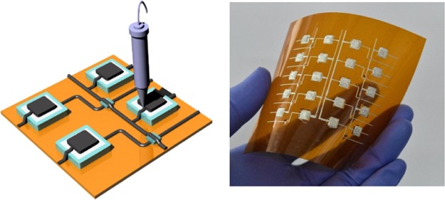
2.4. Three-Dimensional Multistack-Printed, Self-Powered Pressure Sensor Array
Figure 5a is the schematic showing the sequential printing procedure of one sensor part in a 3D multistack-printed array device. An easy way of facilitating the multistack-printing process is to formulate the printable paste with a resistance against gravitational force, which can be evaluated by the values of viscosity and yield stress.37 As another prerequisite, such a thick fluid should undergo a gradual decrease in viscosity in relation to the shear rate to ensure appropriate extrusion during the nozzle-based printing process. For the conductive paste, the solid loading of Ag flake and polymer was regulated from 92 to 97 wt % to formulate a highly viscous, thick fluid. As seen in Figure 5b, the high value of 1.2 × 10⁶ mPa·s in viscosity was measured at a low shear rate, with the value of 290 Pa in yield stress, and then, it decreased to the value of 764.8 mPa·s with increasing a shear rate up to 1000 s–1. In comparison, the two-dimensional screen printable paste has the value of ∼104 mPa·s in viscosity, which is less by a factor of ∼102 than that of the thick paste formulated in this study.
Figure 5.

(a) Schematic showing the sequential multistack-printing process for fabricating the all-printed piezoelectric pressure sensor array; (b) rheological properties of the multistack-printable paste formulated in this study; (c) photograph of the all-printed sensor array device. The scale bar in (c) is 10 mm. (d) Position-addressable voltage output signals measured by a gentle tapping motion on the printed array device.
For the PZT composite paste, a multistack-printable thick paste can be formulated by dispersing well the sophisticatedly surface-functionalized inorganic NPs in a limited amount of solvent. However, air bubbles tend to be trapped in the as-printed layer and are not removed with ease from the pseudo-solid-like wet layer. Alternatively, we printed an insulating bank layer for defining the spatial area where the PZT paste is printed. This method is also advantageous in generating the uniform layer. In overlapping laterally the lines to make a film, a thinner fluid enables to a formation of the even top surface. For printing the bank layer, a viscous PDMS prepolymer was chosen instead of the conventional one, and the same PZT composite paste was used as the one used in bar-coated devices. The rheology properties of the viscous PDMS prepolymer and PZT composite paste are shown in Figure S11. The insulator part was also printed using the viscous PDMS prepolymer for blocking the current flow between adjacent electrode lines. The motion picture showing all printing procedures is seen in Movie S3. As seen in Figure S12, the top Ag electrode lines were formed well along the surface of ∼110 μm thick insulator part and ∼85 μm thick sensor part.
Figure 5c shows a photograph of the complete multistack-printed array device. The output voltage as a function of pressure is shown in Figure S13. The sensitivity of 0.15 V·kPa–1 was measured with an output voltage of 0.21 V at a pressure of 10 kPa, which is slightly lower than that of the bar-coated device. The electrical property of the piezoelectric composite layer sandwiched with lower and upper electrode layers can be mainly influenced by the value in capacitance and the thickness of the dielectric composite layer, as long as the kind of piezoelectric filler is identical. In both bar-coated and printed array devices, the composition of filler particles inside the composite was not altered; thus, it can be presumed that a variation in thickness results in the change in output voltage under given pressure conditions. Controlling the thickness in a uniform film structure is achievable by adjusting the rheological properties of the printable fluid and the processing conditions, namely, parameters in the printing process. More improvement in output voltage in the printed array will be carried out with more delicate preparation of multistack printable pastes and further adjustment of processing variables. Note that, all-printed, self-powered pressure sensor arrays have been rarely reported to date. Most studies have not designed the adequate filler particles and elastomeric matrices that enable for printed piezoelectric composite layers. It is also attributable to the difficulty of fabricating a multistacked device architecture by a sequential printing process. As seen in Figure 5d, in the fully addressable array device, individual output voltage signals were obtained clearly when gentle pressure was imposed on top of designated pixels.
3. Conclusions
We have developed a chemical method of functionalizing chemically the surface of PZT NPs for establishing the electrostatically reinforced heterogeneous interfaces in the piezoelectric composite materials. Through a basic investigation of electrical properties on various chemical and physical elastomers, the SEBSm polymer was chosen as an appropriate elastomeric matrix that can be stable during a high-voltage poling process. The bar-coated devices prepared from SEBSm–PEI-PZT NPs and a mixture of SEBS and SEBSm EPs exhibited a voltage output of 0.8 V at a pressure of 30 kPa, with a linear sensitivity of 0.28 V·kPa–1 in a wide pressure range. The all-printed, self-powered pressure sensor array was also fabricated by carrying out the multistack-printing process of conductive, insulating, and piezoelectric composite pastes.
4. Experimental Details
4.1. Raw Materials
PZT (DPSC-1, Ceracom), Ag flake (1–2 μm, SF-120, Ames Goldsmith Corporation), PDMS (Sylgard 184, Dow Corning), SIS (styrene: 22 wt %, Aldrich), SEBS (Mw: 89,000, Aldrich), and SEBSm (Aldrich), PEI (Mw: 750,000, Aldrich), DCB (98%, Alfa Aesar), and terpineol (95%, Aldrich) were used without further purification. The commercially purchased PZT particles were ball-milled to prepare nanosized PZT particles prior to experiments.
4.2. Preparation of Conductive Composite Pastes
Ag flakes were mixed with a mixture of PDMS prepolymer and a cross-linking agent (ratio by weight = 10:1). The DCB was added and mixed uniformly using a planetary centrifugal mixer (ARE-310, THINKY Corp.). The filler composition of Ag flakes was 92 wt % in a dried film. For the top electrode paste, the DCB was replaced with terpineol to prevent the dissolution of the underlying piezoelectric composite layer. The solid loading of Ag flakes and PDMS was 92 wt % for the paste for the bar-coating process. For the multistack-printable Ag composite paste, the solid loading was regulated up to the value of 97 wt %.
4.3. Preparation of Piezoelectric Composite Pastes
Piezoelectric pastes were prepared with two kinds of PZT NPs. One was pristine PZT NPs, and the other was PZT NPs functionalized chemically with PEI and SEBSm, denoted as SEBSm–PEI-PZT NPs. The pristine PZT NPs were mixed with the elastomer (PDMS, SIS, SEBS, or SEBSm) and DCB, using a planetary centrifugal mixer. The SEBSm–PEI-PZT NPs were synthesized as follows. The PZT NPs were stirred for 60 min in an aqueous PEI solution with the pH of 10 and washed with basic deionized water and ethyl alcohol by a centrifugation technique. The resulting particles were stirred for 30 min in the SEBSm–DCB solution and washed with the toluene using a centrifugation technique. The obtained SEBSm–PEI-PZT NPs were mixed with a mixture of SEBS, SEBSm, and DCB using a planetary centrifugal mixer. In all pastes, the solid loading of PZT NPs and elastomer was 42 wt %, and the filler composition of PZT NPs/(PZT NPs + elastomer) was 80 wt %.
4.4. Fabrication of MIM Devices for Measuring the Leakage Current
Aa 50 nm-thick Cr/Ag bottom electrode was deposited by thermal evaporation on a Si wafer substrate. PDMS, SIS, SEBS, and SEBSm polymer solutions were prepared by mixing with DCB at concentrations of 75, 12, 20, and 10 wt %, respectively. The solutions were spin-coated at a speed of 3000 rpm, followed by thermal annealing at 100 °C for 1 h. Then, the Ag composite paste (solvent: terpineol) was printed and cured at 120 °C for 4 h to complete the PDMS, SEBS, and SEBSm-based MIM devices. For the Ag–PDMS composite electrode, variation in electrical conductivity as a function of curing temperature is shown in Figure S14. The top Ag electrode was evaporated for the SIS-based one.
4.5. Fabrication of Bar-Coated Pressure Sensor Devices
The DCB-based Ag conductive paste was bar-coated on a polyimide (PI) substrate (thickness (t) = 75 μm, Kapton film 300HN, Teijin DuPont Films) with a PI tape side bank (thickness: 125 μm) and cured at 120 °C for 4 h. Then, the piezoelectric pastes were poured on top of the Ag electrode layer with an Ecoflex side bank and dried at room temperature for 2 h and at 100 °C for 1 h. Subsequently, the terpineol-based Ag conductive paste was bar-coated on top of the piezoelectric composite layer with the PI tape side bank and cured at 120 °C for 4 h. The coating speed was 10 mm/s. The film thickness of piezoelectric composite and Ag electrode layers were ∼180 and ∼85 μm, respectively. Both the bottom and top electrode layers were connected with Cu wires and silver epoxy. The poling process was carried out at a voltage of 1000 V for 10 min at room temperature. The voltage output data for the best pressure sensor device are shown in Figure S15 before/after a poling process.
4.6. Fabrication of Multistack-Printed Pressure Sensor Arrays
The printing process was conducted with a three-axis programmable dispenser (Image Master 350PC Smart, Musashi) on the PI substrate. First, the Ag composite paste was printed using a nozzle with an inner diameter of 200 μm under a back pressure of ∼200 kPa on top of the PI substrate. A thermal treatment was carried out at 120 °C for 4 h. The bank layer for confining the spatial area, where the piezoelectric paste is deposited, was formed by printing the viscous PDMS prepolymer (Sylgard 186, Dow Corning) mixed with a cross-liking agent (pre-polymer/cross-linking agent = 10:1 w/w). The inner diameter of the nozzle was 200 μm, and the back pressure was 150–200 kPa. The insulator part was also formed by printing the corresponding PDMS mixture. The PDMS parts were cured at 100 °C for 1 h. Then, the PZT composite paste was printed inside the predefined PDMS bank layer using the nozzle with an inner diameter of 330 μm at a back pressure of ∼20 kPa, followed by a drying process at room temperature for 2 h and at 100 °C for 1 h. The printing speed was 1 mm/s. The film thickness of piezoelectric composite and Ag electrode layers were ∼150 and ∼140 μm, respectively. Finally, the terpineol-based Ag composite paste was printed along the surface of the preformed multilayers and thermal-treated in the same manner as the bottom electrode.
4.7. Characterization
The piezoelectric performance of the sensor devices was measured using an oscilloscope (MDO 3054, Tektronix) and a force gauge (M7-10, Mark-10 Corp.) equipped with a step motor controller (ECOPIA). Pressure was applied to the sensor devices at a pressing rate of 30 mm/s, analogous to that in human activities in our daily lives. The morphologies of the particles and films were observed by SEM (Sigma HD, Carl Zeiss), and the crystal structures of the particles were analyzed by X-ray diffraction (XRD, D/Max-2200V, Rigaku). The surface charge of the particles was measured with a zeta-potential analyzer (ELS-Z, Otsuka), and the chemical groups of functionalized particles were investigated by FT-IR spectroscopy (Carry 5000, Varian). The glass transition temperature was measured by differential scanning calorimetry (DSC Q1000, TA). The leakage current behaviors were measured with a semiconductor parameter analyzer (E5270B, Agilent) equipped with a probe station. In measuring the electrical properties, the patterned upper electrodes were formed by a dispensing printing process of Ag paste or by a thermal evaporation of the Ag metal through the metal mask. The sheet resistance was measured with a 4-point probe (RSD-40K, DASOENG).
Acknowledgments
This research was supported by the Global Research Laboratory Program of the National Research Foundation (NRF) funded by Ministry of Science, Information and Communication Technologies and Future Planning (NRF-2015K1A1A2029679) and partially supported by the Nano·Material Technology Development Program through the National Research Foundation of Korea funded by the Ministry of Science, Information, and Communication Technologies and Future Planning (NRF-2015M3A7B4050306). This work was also supported by Creative Materials Discovery Program through the National Research Foundation of Korea (NRF) funded by Ministry of Science and ICT (NRF-2019M3D1A2103917).
Supporting Information Available
The Supporting Information is available free of charge at https://pubs.acs.org/doi/10.1021/acsomega.9b03753.
SEM image and XRD result of pristine PZT NPs, an evolution of conductivity depending on the curing condition in the Ag–PDMS composite electrode, current density–electric field data for SIS, SBES, SEBS, and PDMS layers, piezoelectric performance of pPDMS devices with polymeric matrices with various elastic moduli, cross-sectional SEM image of the optimized bar-coated sensor layer, the variation in device performance depending on the composition of filler particle, rheological properties of printable insulator and piezoelectric composite paste, photographs and voltage output data of the all-printed sensor array device, and motion pictures showing the device operation and sequential printing processes (PDF)
Measuring a very gentle touch pressure with clear voltage signals (MOV)
Distinguishing clearly pressure difference in gentle and mild tapping motions with a difference of ∼3 V in output voltage (MOV)
Motion picture showing all printing procedures (MP4)
The authors declare no competing financial interest.
Supplementary Material
References
- Zang Y.; Zhang F.; Di C.-a.; Zhu D. Advances of Flexible Pressure Sensors toward Artificial Intelligence and Health Care Applications. Mater. Horiz. 2015, 2, 140–156. 10.1039/c4mh00147h. [DOI] [Google Scholar]
- Li J.; Bao R.; Tao J.; Peng Y.; Pan C. Recent Progress in Flexible Pressure Sensor Arrays: from Design to Applications. J. Mater. Chem. C 2018, 6, 11878–11892. 10.1039/c8tc02946f. [DOI] [Google Scholar]
- Boutry C. M.; Kaizawa Y.; Schroeder B. C.; Chortos A.; Legrand A.; Wang Z.; Chang J.; Fox P.; Bao Z. A Stretchable and Biodegradable Strain and Pressure Sensor for Orthopedic Application. Nat. Electron. 2018, 1, 314–321. 10.1038/s41928-018-0071-7. [DOI] [Google Scholar]
- Boutry C. M.; Nguyen A.; Lawal Q. O.; Chortos A.; Rondeau-Gagné S.; Bao Z. A Sensitive and Biodegradable Pressure Sensor Array for Cardiovascular Monitoring. Adv. Mater. 2015, 27, 6954–6961. 10.1002/adma.201502535. [DOI] [PubMed] [Google Scholar]
- Kim J.; Lee M.; Shim H. J.; Ghaffari R.; Cho H. R.; Son D.; Jung Y. H.; Soh M.; Choi C.; Jung S.; Chu K.; Jeon D.; Lee S. T.; Kim J. H.; Choi S. H.; Hyeon T.; Kim D.-H. Stretchable Silicon Nanoribbon Electronics for Skin Prosthesis. Nat. Commun. 2014, 5, 5747–5757. 10.1038/ncomms6747. [DOI] [PubMed] [Google Scholar]
- Chen L. Y.; Tee B. C. K.; Chortos A. L.; Schwartz G.; Tse V.; Lipomi D. J.; Wong H. S. P.; McConnell M. V.; Bao Z. Continuous Wireless Pressure Monitoring and Mapping with Ultra-Small Passive Sensors for Health Monitoring and Critical Care. Nat. Commun. 2014, 5, 5028–5037. 10.1038/ncomms6028. [DOI] [PubMed] [Google Scholar]
- Kim C.-C.; Lee H.-H.; Oh K. H.; Sun J.-Y. Highly Stretchable, Transparent Ionic Touch Panel. Science 2016, 353, 682–687. 10.1126/science.aaf8810. [DOI] [PubMed] [Google Scholar]
- Jin M. L.; Park S.; Lee Y.; Lee J. H.; Chung J.; Kim J. S.; Kim J.-S.; Kim S. Y.; Jee E.; Kim D. W.; Chung J. W.; Lee S. G.; Choi D.; Jung H.-T.; Kim D. H. An Ultrasensitive, Visco-Poroelastic Artificial Mechanotransducer Skin Inspired by Piezo2 Protein in Mammalian Merkel Cells. Adv. Mater. 2017, 29, 1605973. 10.1002/adma.201605973. [DOI] [PubMed] [Google Scholar]
- Lee J.-H.; Yoon H.-J.; Kim T. Y.; Gupta M. K.; Lee J. H.; Seung W.; Ryu H.; Kim S.-W. Micropatterned P(VDF-TrFE) Film-Based Piezoelectric Nanogenerators for Highly Sensitive Self-Powered Pressure Sensors. Adv. Funct. Mater. 2015, 25, 3203–3209. 10.1002/adfm.201500856. [DOI] [Google Scholar]
- Chen X.; Tian H.; Li X.; Shao J.; Ding Y.; An N.; Zhou Y. A High Performance P(VDF-TrFE) Nanogenerator with Self-Connected and Vertically Integrated Fibers by Patterned EHD Pulling. Nanoscale 2015, 7, 11536–11544. 10.1039/c5nr01746g. [DOI] [PubMed] [Google Scholar]
- Persano L.; Dagdeviren C.; Su Y.; Zhang Y.; Girardo S.; Pisignano D.; Huang Y.; Rogers J. A. High Performance Piezoelectric Devices based on Aligned Arrays of Nanofibers of Poly(Vinylidenefluoride-co-Trifluoroethylene). Nat. Commun. 2013, 4, 1633–1642. 10.1038/ncomms2639. [DOI] [PubMed] [Google Scholar]
- Shin K.-Y.; Lee J. S.; Jang J. Highly Sensitive, Wearable and Wireless Pressure Sensor Using Free-Standing ZnO Nanoneedle/PVDF Hybrid Thin Film for Heart Rate Monitoring. Nano Energy 2016, 22, 95–104. 10.1016/j.nanoen.2016.02.012. [DOI] [Google Scholar]
- Xu M.; Kang H.; Guan L.; Li H.; Zhang M. Facile Fabrication of a Flexible LiNbO3 Piezoelectric Sensor through Hot Pressing for Biomechanical Monitoring. ACS Appl. Mater. Interfaces 2017, 9, 34687–34695. 10.1021/acsami.7b10411. [DOI] [PubMed] [Google Scholar]
- Chen X.; Parida K.; Wang J.; Xiong J.; Lin M.-F.; Shao J.; Lee P. S. A Stretchable and Transparent Nanocomposite Nanogenerator for Self-Powered Physiological Monitoring. ACS Appl. Mater. Interfaces 2017, 9, 42200–42209. 10.1021/acsami.7b13767. [DOI] [PubMed] [Google Scholar]
- Deutz D. B.; Mascarenhas N. T.; Schelen J. B. J.; de Leeuw D. M.; van der Zwaag S.; Groen P. Flexible Piezoelectric Touch Sensor by Alignment of Lead-Free Alkaline Niobate Microcubes in PDMS. Adv. Funct. Mater. 2017, 27, 1700728. 10.1002/adfm.201700728. [DOI] [Google Scholar]
- Chung S. Y.; Lee H.-J.; Lee T. I.; Kim Y. S. A Wearable Piezoelectric Bending Motion Sensor for Simultaneous Detection of Bending Curvature and Speed. RSC Adv. 2017, 7, 2520–2526. 10.1039/c6ra25797f. [DOI] [Google Scholar]
- Fan F. R.; Tang W.; Wang Z. L. Flexible Nanogenerators for Energy Harvesting and Self-Powered Electronics. Adv. Mater. 2016, 28, 4283–4305. 10.1002/adma.201504299. [DOI] [PubMed] [Google Scholar]
- Chen X.; Xiong J.; Parida K.; Guo M.; Wang C.; Wang C.; Li X.; Shao J.; Lee P. S. Transparent and Stretchable Bimodal Triboelectric Nanogenerators with Hierarchical Micro-Nanostructures for Mechanical and Water Energy Harvesting. Nano Energy 2019, 64, 103904. 10.1016/j.nanoen.2019.103904. [DOI] [Google Scholar]
- Park K.-I.; Lee M.; Liu Y.; Moon S.; Hwang G.-T.; Zhu G.; Kim J. E.; Kim S. O.; Kim D. K.; Wang Z. L.; Lee K. J. Flexible Nanocomposite Generator Made of BaTiO3 Nanoparticles and Graphitic Carbons. Adv. Mater. 2012, 24, 2999–3004. 10.1002/adma.201200105. [DOI] [PubMed] [Google Scholar]
- Park K.-I.; Jeong C. K.; Ryu J.; Hwang G.-T.; Lee K. J. Flexible and Large-Area Nanocomposite Generators Based on Lead Zirconate Titanate Particles and Carbon Nanotubes. Adv. Energy Mater. 2013, 3, 1539–1544. 10.1002/aenm.201300458. [DOI] [Google Scholar]
- Chen X.; Li X.; Shao J.; An N.; Tian H.; Wang C.; Han T.; Wang L.; Lu B. High-Performance Piezoelectric Nanogenerators with Imprinted P(VDF-TrFE)/BaTiO3 Nanocomposites Micropillars for Self-Powered Flexible Sensors. Small 2017, 13, 1604245. 10.1002/smll.201604245. [DOI] [PubMed] [Google Scholar]
- Chen X.; Shao J.; An N.; Li X.; Tian H.; Xu C.; Ding Y. Self-Powered Flexible Pressure Sensors with Vertically Well-Aligned Piezoelectric Nanowire Arrays for Monitoring Vital Signs. J. Mater. Chem. C 2015, 3, 11806–11814. 10.1039/c5tc02173a. [DOI] [Google Scholar]
- Xie M.; Zhang Y.; Kraśny M. J.; Bowen C.; Khanbareh H.; Gathercole N. Flexible and Active Self-Powered Pressure, Shear Sensors Based on Freeze Casting Ceramic-Polymer Composites. Energy Environ. Sci. 2018, 11, 2919–2927. 10.1039/c8ee01551a. [DOI] [PMC free article] [PubMed] [Google Scholar]
- Park D. Y.; Joe D. J.; Kim D. H.; Park H.; Han J. H.; Jeong C. K.; Park H.; Park J. G.; Joung B.; Lee K. J. Self-Powered Real-Time Arterial Pulse Monitoring Using Ultrathin Epidermal Piezoelectric Sensors. Adv. Mater. 2017, 29, 1702308. 10.1002/adma.201702308. [DOI] [PubMed] [Google Scholar]
- Cao Q.; Hur S.-H.; Zhu Z.-T.; Sun Y. G.; Wang C.-J.; Meitl M. A.; Shim M.; Rogers J. A. Highly Bendable, Transparent Thin-Film Transistors That Use Carbon-Nanotube-Based Conductors and Semiconductors with Elastomeric Dielectrics. Adv. Mater. 2006, 18, 304–309. 10.1002/adma.200501740. [DOI] [Google Scholar]
- Raveendran R.; Namboothiry M. A. G. Surface-Treated Poly(dimethylsiloxane) as a Gate Dielectric in Solution-Processed Organic Field-Effect Transistors. ACS Omega 2018, 3, 11278–11285. 10.1021/acsomega.8b01629. [DOI] [PMC free article] [PubMed] [Google Scholar]
- Choi S.; Han S. I.; Kim D.; Hyeon T.; Kim D. H. High-Performance Stretchable Conductive Nanocomposites: Materials, Processes, and Device Applications. Chem. Soc. Rev. 2019, 48, 1566–1595. 10.1039/c8cs00706c. [DOI] [PubMed] [Google Scholar]
- Cho S.; Song J. H.; Kong M.; Shin S.; Kim Y.-T.; Park G.; Park C.-G.; Shin T. J.; Myoung J.; Jeong U. Fully Elastic Conductive Films from Viscoelastic Composites. ACS Appl. Mater. Interfaces 2017, 9, 44096–44105. 10.1021/acsami.7b14504. [DOI] [PubMed] [Google Scholar]
- Maliakal A.; Katz H.; Cotts P. M.; Subramoney S.; Mirau P. Inorganic Oxide Core, Polymer Shell Nanocomposite as a High K Gate Dielectric for Flexible Electronics Applications. J. Am. Chem. Soc. 2005, 127, 14655–14662. 10.1021/ja052035a. [DOI] [PubMed] [Google Scholar]
- Facchetti A.; Yoon M.-H.; Marks T. J. Gate Dielectrics for Organic Field-Effect Transistors: New Opportunities for Organic Electronics. Adv. Mater. 2005, 17, 1705–1725. 10.1002/adma.200500517. [DOI] [Google Scholar]
- Wang N.; Hsu C.; Zhu L.; Tseng S.; Hsu J.-P. Influence of Metal Oxide Nanoparticles Concentration on their Zeta Potential. J. Colloid Interface Sci. 2013, 407, 22–28. 10.1016/j.jcis.2013.05.058. [DOI] [PubMed] [Google Scholar]
- Chae C.; Kim K. W.; Yun Y. J.; Lee D.; Moon J.; Choi Y.; Lee S. S.; Choi S.; Jeong S. Polyethylenimine-Mediated Electrostatic Assembly of MnO2 Nanorods on Graphene Oxides for Use as Anodes in Lithium-Ion Batteries. ACS Appl. Mater. Interfaces 2016, 8, 11499–11506. 10.1021/acsami.6b01931. [DOI] [PubMed] [Google Scholar]
- Schmidt U.; Zschoche S.; Werner C. Modification of Poly(octadecene-alt-maleic anhydride) Films by Reaction with Functional Amines. J. Appl. Polym. Sci. 2003, 87, 1255–1266. 10.1002/app.11527. [DOI] [Google Scholar]
- Yoon M.-H.; Kim C.; Facchetti A.; Marks T. J. Gate Dielectric Chemical Structure-Organic Field-Effect Transistor Performance Correlations for Electron, Hole, and Ambipolar Organic Semiconductors. J. Am. Chem. Soc. 2006, 128, 12851–12869. 10.1021/ja063290d. [DOI] [PubMed] [Google Scholar]
- Wu H.; Huang B.; Zare R. N. Construction of Microfluidic Chips Using Polydimethylsiloxane for Adhesive Bonding. Lab Chip 2005, 5, 1393–1398. 10.1039/b510494g. [DOI] [PubMed] [Google Scholar]
- Chau K.; Millare B.; Lin A.; Upadhyayula S.; Nuñez V.; Xu H.; Vullev V. I. Dependence of the Quality of Adhesion between Poly(dimethylsiloxane) and Glass Surfaces on the Composition of the Oxidizing Plasma. Microfluid. Nanofluid. 2011, 10, 907–917. 10.1007/s10404-010-0724-y. [DOI] [Google Scholar]
- Lewis J. A. Colloidal Processing of Ceramics. J. Am. Ceram. Soc. 2000, 83, 2341–2359. 10.1111/j.1151-2916.2000.tb01560.x. [DOI] [Google Scholar]
Associated Data
This section collects any data citations, data availability statements, or supplementary materials included in this article.