

Abstract

Organic photovoltaics are a sustainable and cost-effective power-generation technology that may aid the move to zero-emission buildings, carbon neutral cities, and electric vehicles. While state-of-the-art organic photovoltaic devices can be encapsulated to withstand air and moisture, they are currently still susceptible to light-induced degradation, leading to a decline in the long-term efficiency of the devices. In this study, the role of ultraviolet (UV) radiation on a multilayer organic photovoltaic device is systematically uncovered using spectral filtering. By applying long-pass filters to remove different parts of the UV portion of the AM1.5G spectrum, two main photodegradation processes are shown to occur in the organic photovoltaic devices. A UV-activated process is found to cause a significant decrease in the photocurrent across the whole spectrum and is most likely linked to the deterioration of the charge extraction layers. In addition, a photodegradation process caused by UV-filtered sunlight is found to change the micromorphology of the bulk heterojunction material, leading to a reduction in photocurrent at high photon energies. These findings strongly suggest that the fabrication of inherently photostable organic photovoltaic devices will require the replacement of fullerene-based electron transporter materials with alternative organic semiconductors.
Keywords: charge-transfer state, electroluminescence spectroscopy, photocurrent spectroscopy, external quantum efficiency, stability
1. Introduction
Photovoltaic devices have made significant inroads into becoming one of the more prominent renewable energy-harvesting technologies.1 Silicon-based photovoltaic modules can be readily found in solar farms and on top of roofs across the world, owing to their low cost of production and high efficiency. However, these modules are heavy, require energy-intensive fabrication processes, and can be aesthetically unappealing.2 On the other hand, organic-semiconductor-based photovoltaics can be fabricated on lightweight substrates, made with varying levels of transparency and have a low energy-payback time.3 These qualities make them an attractive option as an energy source in zero-emission buildings, public places, and vehicles.3 Organic semiconductors provide a versatile chemical framework, which can be finely tuned to optimize properties, such as band gap and miscibility, and to reduce toxicity.4 Two main types of organic semiconductors are currently used in photovoltaic devices, which are small organic molecules such as fullerenes and polymer-based semiconductors such as poly(3-hexylthiophene-2,5-diyl). Fullerenes are usually chosen as the electron acceptor material because of their well-known processing conditions and favorable band alignment with the donor polymer, allowing for efficient charge transfer (CT).5 Polymeric and small organic molecular semiconductors can be used in combination to form either a planar heterojunction device or a bulk heterojunction (BHJ) device. The interface between the donor and acceptor materials in an organic photovoltaic (OPV) device creates an energy offset that allows the photoexcited species, bound electron–hole pairs (excitons), to overcome the large binding energy (Eb).6 A bulk heterojunction film is formed when the acceptor and donor materials are dissolved in a single solution, which is cast to create a thin film that contains a blend of both materials. The profile of the interface between the acceptor and donor materials creates a large interfacial surface area, allowing excitons to be within the diffusion length of the interface.7 Because the heterojunction creates segregated domains whose dimensions are shorter than the exciton diffusion length, BHJ-based photovoltaic devices have a high internal quantum efficiency (EQE), as most excitons are dissociated and collected at the electrodes.8 Therefore, the morphology of the heterojunction plays a key role in ensuring that the device is performing at its maximum potential.9
Currently, the most significant hurdle to the commercialization of OPV devices is their long-term stability, which must be improved to ensure they are an effective alternative to silicon photovoltaics. Ambient air, specifically moisture and oxygen, has been observed to impact the stability of OPV devices.10 Upon absorption of oxygen from ambient air, the metal electrodes can react with the oxygen to form an oxide, creating a barrier for charge extraction, which reduces the power conversion efficiency (PCE).11 The photoactive layer has also shown to readily absorb moisture, and upon illumination, photochemical reactions can cause an increase in trap density in the polymer layer.12 An increase in trap density will increase charge-carrier recombination, reducing the PCE of the device.13 Furthermore, exposure to moisture and oxygen during device processing can cause a significant change in the morphology of the BHJ interface, leading to a reduction in device performance.14
Nevertheless, by processing devices in an inert atmosphere and through recent improvements in encapsulation techniques, the impact of ambient air on the degradation of OPV devices has been reduced.10,15 Despite protection from air, OPV devices under constant light illumination show a sharp initial decrease, followed by a slower and steady decline in the power conversion efficiency (PCE). This initial period has been termed the “burn-in period”, during which devices show a decrease in current–voltage (J–V) parameters such as the short-circuit current density (Jsc), open-circuit voltage (Voc), fill factor, and power conversion efficiency.15 The photoactivated changes that occur in encapsulated OPV devices affect the micromorphology of the BHJ and initiate unwanted chemical reactions of either the donor or acceptor, mainly affecting the short-circuit current density (Jsc) and the open-circuit voltage (Voc).16−19 It is well known that fullerenes form oligomers when exposed to light, causing the PCE to drop because such fullerene oligomers exhibit shorter exciton diffusion lengths and lower charge-carrier mobilities compared to the initially isolated fullerenes.20−22 However, oligomerization can potentially be avoided by ensuring that the BHJ comprises crystalline fullerene domains forming a blend with the donor polymer.16
Another factor that may be affected by degradation is the nature of the electronic states at the bulk heterojunction interface. OPVs are excitonic at room temperature owing to the enhanced coulombic interaction between the electrons and holes, resulting in an exciton binding energy (Eb) that is on the order of ∼100 meV.23 At the interface between the acceptor and donor materials, the acceptor material, usually fullerene-based, has a higher electron affinity than the donor material, which creates an energy offset that allows electrons to overcome the exciton binding energy.24 However, a proportion of dissociated charge carriers may continue to interact with each other across the interface such that the frontier orbitals of the allowed electronic states between the highest occupied molecular orbital of the donor (HOMOdonor) and the lowest unoccupied molecular orbital of the acceptor (LUMOacceptor) overlap.25,26 Such interfacial charge-transfer (CT) states are bound states formed between a hole residing on the donor polymer and an electron on the acceptor. Random diffusion of a CT excitation in the vicinity of the interface, assisted by the internal field, will eventually lead to either charge separation or recombination.25,27 The energy of the CT state, ECT, can be deduced using absorption- and emission-based spectroscopic techniques.28 However, the intensity of the photocurrent signal from the CT state is usually orders of magnitude lower than that associated with excitons residing on only the donor polymer.29 An accurate assessment of such CT states is essential because the choice of the donor and acceptor molecules and the morphology of the BHJ can significantly influence the spatial delocalization of the CT state, which will alter the dissociation efficiency of electrons and holes into free carriers.27,30,31
A typical OPV device consists of a thin-film stack that includes the photoactive layer (PAL), the electrodes, and the charge transport layers that ensure selective extraction of electrons and holes towards the opposing electrodes. An example of a typical hole transport material is poly(3,4-ethylenedioxythiophene):poly(styrene sulfonate) (PEDOT:PSS), notable for its transparency in the visible spectrum and its high electric conductivity.32 Photodegradation, in particular, ultraviolet (UV)-induced photodegradation, may therefore affect a multitude of layers in an OPV device, rather than just the PAL. For example, Sapkota et al. observed that when OPV devices were exposed to UV radiation for 2000 h, the electrical conductivity of the PEDOT:PSS hole transport layer (HTL) was drastically reduced, while the PAL showed little degradation.33 To combat UV-induced photodegradation, UV filters have been placed either within the device or as a filter on top, which resulted in a significant improvement in the photostability of encapsulated OPV devices.34,35 An investigation of light-induced photodegradation, with a particular focus on the changes in the sub-band-gap photocurrent spectra during the burn-in period, has the potential to clarify how standard solar and UV-filtered solar light cause photodegradation in the different layers of an OPV device. Changes in the sub-band-gap photocurrent spectra can be indicative of effects on the micromorphology of the BHJ,31,36 while any degradation observed in the overall photocurrent spectra can elucidate macroscopic alterations of the charge transport layers.37
In this study, we use the highly sensitive technique of Fourier transform photocurrent spectroscopy (FTPS) to investigate spectral changes in the external quantum efficiency (EQE) induced in organic photovoltaic BHJ devices during midterm exposure to filtered and unfiltered light from a solar simulator. We track the photoinduced degradation in the short-circuit current during the burn-in period while illuminating the device with an air mass 1.5G (AM1.5) spectrum continuously for 18 h and periodically measuring the EQE spectra. By taking advantage of the sensitivity of FTPS, we are able to resolve clear changes in the sub-band-gap photocurrent during device aging with UV-filtered light. Using electroluminescence (EL) spectroscopy, we identify a charge-transfer state of energy ECT = 1.31 eV and conclude that the observed changes in the sub-band-gap photocurrent originate from a mechanism coupled to the CT state, most likely oligomerization of the fullerenes. We also find that exposure to unfiltered light leads to photodegradation that affects the whole photocurrent spectrum, which we attribute to degradation processes affecting the electrode materials.
2. Results
Figure 1a illustrates the structure of the OPV devices investigated in this study. The donor material, PBTZT-stat-BDTT-8,38 is based on a conjugated polymer whose backbone consists of substituted thiophenes with side chains enhancing the solubility of the polymer.39 The acceptor molecule is phenyl-C61-butyric-acid-methyl-ester (PCBM), a functionalized fullerene that is commonly used in BHJ films because of its solubility in a wide range of solvents, suitable energetic alignment with the donor polymer, and a delocalized LUMO allowing for favorable electron mobilities.40 The material combination used in the photoactive layer has previously been shown to be versatile in different solvent systems and device architectures and to yield OPV devices with a power conversion efficiency (PCE) of 9.3%.38 Electron and hole extraction layers were based on polymers PV-E002 and PEDOT:PSS.38 The current–voltage characteristics for the complete set of devices investigated in this study are provided in Figures S1 and S6 (Supporting Information).
Figure 1.
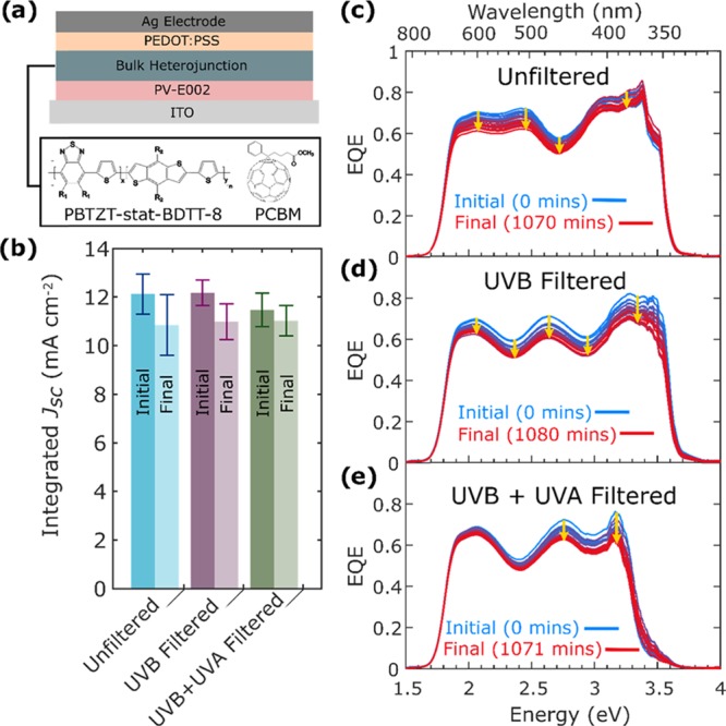
(a) Device schematic for the OPV devices investigated in this study. The bulk heterojunction consists of the donor polymers PBTZT-stat-BDTT-8 and PCBM, and the electron and hole transport layers of polymer PV-E00238 and PEDOT:PSS, respectively, as described previously.38 (b) Mean short-circuit current densities (Jsc) deduced from the initial EQE spectra and the final spectra after 1070 min of exposure to AM1.5 light with or without filters (averaged over three or more devices). (c–e) Changes in external quantum efficiency (EQE) when the device is illuminated with AM1.5, 0.7 sunlight (70 mW cm–2) that is (c) unfiltered, (d) UVB-filtered (280 ≤ λ < 315 nm) by long-pass (LP) H-BaK7 glass 331 nm (331-GY Comar Optics), and (e) UVB + UVA-filtered (280 ≤ λ < 400 nm) with long pass (LP).
Characterization of solar cells under illumination is based upon a light source that represents the spectral irradiance upon Earth when the sun is 48.19° from the zenith. This so-called air mass 1.5G (AM1.5) spectrum is corrected for solar irradiation that is absorbed or scattered when light travels through the earth’s atmosphere. While the atmosphere absorbs a significant portion of the UV radiation from the sun, a small quantity still reaches the earth’s surface (see Figure S2).41,42 To investigate the effect of UV radiation on OPV devices, we use long-pass (LP) filters to systematically block different categories of UV light from the AM1.5 spectrum generated by a solar simulator (Figure S2). ISO classification splits UV light into two distinct ranges within the AM1.5 solar spectrum, UVB (280 ≤ λ < 315 nm) and UVA (315 ≤ λ < 400 nm).43 We used two long-pass filters, LP 331 nm, which filters only UVB light, and LP 400 nm, which filters both UVB and UVA from the AM1.5 solar spectrum. Figure S2 shows the relative intensities of both the UVB and UVA components in the AM1.5 solar spectrum, together with the transmission functions of the long-pass filters.
To investigate the mechanism by which light causes device degradation, we track the changes in the EQE spectra as a function of illumination time over 18 h, for the three scenarios of unfiltered, UVB-filtered, and UVB + UVA-filtered light. Figure 1b shows the mean initial and the final values of the integrated short-circuit current densities (Jsc) extracted from the EQE spectra. Initial Jsc values vary between the three filtration conditions because of differences in the reduction of photon flux. When both UVB + UVA components are eliminated from the spectrum, the initial Jsc is significantly lowered, while for filtration of only UVB, little change is evident compared with full AM1.5 exposure. These differences simply reflect the fact that there is a very small component of UVB light contained in the AM1.5 spectrum (see Figure S2), which will, in any case, also be partly absorbed by the glass substrate and the indium-tin-oxide electrode.44 As a result, the introduction of a 331 nm long-pass filter (to filter UVB) does not significantly reduce the rate of device degradation, as evident from Figure 1b.
To illustrate how differences in spectral filtration of the incident light affect the photocurrent for different incident photon energies, we show in Figure 1c the EQE spectra recorded for three devices that were constantly illuminated by 0.7 sun (70 mW cm–2) unfiltered AM1.5 light, only UVB-filtered AM1.5 light, and both UVB + UVA-filtered AM1.5 light. The slight difference in the spectral profile of the EQE between the devices results from them forming low finesse electrooptical cavities.45 Hence, slight changes in the thickness of the photoactive layer will result in a different optical interference pattern within the device.45 It is evident that under all three conditions, the EQE spectra shift downwards over the duration of the light exposure. The device exposed to unfiltered AM1.5 light shows the largest decrease in EQE over 1070 min, with the device exposed to just UVB-filtered light again showing very similar effects. However, for the device exposed to UVB + UVA-filtered AM1.5 light, degradation is much reduced. In addition, while both unfiltered and UVB-filtered light exposure result in an overall downward shift in EQE across the whole spectrum, the device exposed to UVB + UVA-filtered AM1.5 light exhibits a larger decrease in EQE at higher photon energies and a minimal reduction in EQE at photon energies below 2.5 eV. Therefore, it appears that light with wavelengths shorter than 400 nm triggers one UV-activated degradation mechanism that causes an overall reduction in EQE across the whole spectrum, while a second photodegradation process can occur in the presence of light even without a UV component, which leads to a decrease in EQE only at higher photon energies. As we show below, the latter process is linked to dimerization of PCBM and hence it mostly affects the EQE at photon energies above 2.25 eV (λ = 550 nm) where PCBM absorbs.46 While the PCBM absorbs in the visible region (550–400 nm), photochemical reactions that trigger dimerization occur predominantly from UV light, due to the high absorption coefficient of PCBM above 400 nm.47,48 Previous studies have shown that dimerization of PCBM will decrease the exciton diffusion length and charge-carrier mobility, leading to a reduction of device Jsc.16,20,21,49,50 Therefore, such dimerization can significantly affect both light absorption in the PCBM spectral region and charge extraction from the device. Furthermore, all exposure conditions result in a fast initial loss in EQE. The fast initial loss in EQE correlates well with trends observed previously, which have shown that there is a fast decrease in Jsc during the burn-in period of OPV devices consisting of fullerene-based acceptor molecules.15
We explore the temporal dynamics of device degradation by plotting the integrated Jsc, extracted from the EQE spectra, for the devices as they are exposed to unfiltered AM1.5 and UVB + UVA-filtered AM1.5 light over 18 h (Figure 2). From now on, we focus the study on these two conditions only because the filtration of only UVB light was shown to result in little change compared with exposure to unfiltered AM1.5 light. Figure 2 shows that the rate of photoinduced degradation is slowed when UVB and UVA light are filtered from the AM1.5 spectrum. While both devices exhibit the typical17 burn-in period of OPV devices within the first 10 h, the decrease in Jsc proceeds at different rates, similar to trends previously observed in power conversion efficiencies.49 To obtain numerical values for the degradation rates, we fitted an exponential function to the integrated Jsc and extracted the time T90 taken for the Jsc to reach 90% of its initial value.51 We find that for UVB + UVA-filtered AM1.5 light, the device exhibits a T90 lifetime of ∼1600 min, 53% longer than for the device exposed to unfiltered AM1.5 light (∼1050 min). Therefore, while the addition of a long-pass 400 nm filter reduces the initial Jsc through the reduction of photon flux, this detrimental effect is largely compensated after the first ∼18 h because of the reduced rate of burn-in degradation.
Figure 2.

Change in spectrally integrated current density (Jsc), blue crosses, calculated from integration of the EQE spectra (Figure 1) and the Jsc normalized with respect to the initial Jsc, red circles, for OPV devices exposed to unfiltered and UVB + UVA-filtered AM1.5 light. The normalized data is fitted with the expression A e–Bt, with A and B as fitting parameters. The values T90 indicate the time taken for the devices to reach 90% of the initial Jsc, as extracted from the fits. The green shaded region indicates the 98% confidence interval of the fit. Each data point is derived from a full EQE spectrum taken at that time.
To explore further why UVB + UVA-filtered light may still cause a sizeable amount of degradation to the devices, we examined more closely the spectral changes occurring in EQE as a result of such illumination. Figure 1c already demonstrated that the device exposed to UVB + UVA-filtered AM1.5 light displayed a reduction in EQE at higher photon energies where PCBM absorbs, suggesting a link with changes in this component. To examine whether this reduction in EQE is caused by the oligomerization of PCBM, we carefully explore any additional changes that may occur below the band gap Eg, where CT state photocurrent features may contribute.52−54 Because the CT state arises from an overlap between the frontier molecular orbitals of the acceptor and the donor, even a minute change in the morphology of the heterojunction, caused, e.g., by the oligomerization of PCBM, will affect the number of free charges generated from the CT state. Figure S3 displays the sub-band-gap EQE of the initial and final EQE spectra of devices exposed to unfiltered AM1.5 light and alternatively to UVB + UVA-filtered AM1.5 light. A notable difference in the initial and final photocurrent spectra recorded under the two illumination conditions can be clearly seen once the spectra are plotted on a semilogarithmic scale. While the device exposed to UVB + UVA-filtered AM1.5 light suffers from a reduction in sub-band-gap photocurrent after 1070 min, the device exposed to unfiltered AM1.5 light shows no change.
To confirm whether the observed sub-band-gap photocurrent is indeed generated by dissociated charges from the CT state, we record electroluminescence (EL) spectra for a device and correlate the recorded features with those observed in the EQE spectra.55 During EL, electrons are injected from the electrodes into the LUMOacceptor and holes into the HOMOdonor levels, leading to a gradual population of the available density of states, starting with the lowest-energy states.56 When the device is under forward bias, charges will diffuse toward the heterojunction where they may be captured into CT states through which they may radiatively recombine. The EL spectrum generated at low biases will represent the distribution of states that correspond to the charge-transfer state, where the peak will represent the energy ECT of the CT state.55Figure 3 shows the bias-dependent EL spectra recorded for both a fresh device and an aged device, which had been illuminated for 1070 min with a UVB + UVA-filtered AM1.5 light. As the voltage is increased, more charge carriers are injected into the device, leading to an increase in radiative recombination events and hence an observed rise in EL intensity. To determine the difference in energy between the emitting excited state and the ground state, we fitted Gaussians to the EL spectra to determine the peak EL energy, with the resulting values shown in Figure 3c as a function of the bias voltage. As the bias voltage is increased from 1.0 to 1.5 V, the peak energy of the EL spectrum rises because minority tail states associated with the CT state are increasingly populated until they are filled. However, beyond a certain bias (1.6 V for the fresh and 1.8 V for the aged device), the peak energy stabilizes, and the only further change in the EL spectra (Figure 3a,b) is a rise in peak intensity. Hence, at this point, the stabilized EL spectra can be attributed to the prominent CT state, which has a peak energy of ECT = 1.31 eV, as apparent from the bias-independent regime shown by the dashed green line in Figure 3c.
Figure 3.

Electroluminescence spectra and the corresponding Gaussian fits, for an OPV device under different bias voltages recorded for the case that the device was (a) fresh, i.e., without any aging, (b) aged under UVB + UVA-filtered AM1.5 light for 1070 min. (c) Peak energy of the EL versus the applied bias, extracted from Gaussian fits to the EL spectra, for the fresh device (blue) and the aged device (red). More details on the applied voltage versus current density can be found in Figure S7 in the Supporting Information.
To correlate the extracted stabilized EL spectra with the EQE spectra, Figure 4 displays spectra, both in the same graph, for a fresh device and after it has been aged under UVB + UVA-filtered AM1.5 light for 1071 min. The graph shows clear correlations, in terms of both the spectral positions of the features observed in the EL and subgap EQE, and the changes found upon aging. Both features are centered around the energy ECT = 1.31 eV of the CT state, and both show a similar relative decline in signal intensity as the device is aged. We therefore demonstrate that device aging under UVB + UVA-filtered AM1.5 light has a direct effect on the CT state at the PBTZT-stat-BDTT-8/PCBM interface.
Figure 4.

Electroluminescence (EL) spectra and solar cell EQE spectra displayed together on a semilogarithmic scale. The blue lines represent the initial scan taken on a fresh device, and the red and pink lines represent the final spectra taken after the devices had been exposed to UVB + UVA-filtered AM1.5 light for 1071 min. The EL of the fresh and aged devices were taken for an injection current of ∼17.5 mA cm–2 at stabilized conditions (1.6 V for fresh and 1.8 V for aged devices) and show peak luminescence near 1.31 and 1.30 eV, respectively. The arrows represent the y-axis that the data corresponds to. The peak energy of the charge-transfer state (ECT), derived from a Gaussian fit of the EL spectra (dashed lines), corresponds to the photon energy at which a sub-band-gap decrease in EQE is observed for the device, clearly indicating that the decrease in sub-band-gap photocurrent is associated with the CT state.
3. Discussion
The above results suggest that there are two degradation mechanisms operating during the initial burn-in process, one that does not require a UV component of the light and affects mostly the high-energy end of the EQE spectrum, and another that reduces the EQE across the spectrum in the presence of UV.
As we have argued above, the observed photodegradation in the presence of UVB + UVA-filtered AM1.5 light is predominantly caused by changes in the PCBM component that also affect the CT states formed at the PBTZT-stat-BDTT-8/PCBM heterojunction. We attribute the cause of this light-induced change to oligomerization of PCBM, which has been shown to reduce both exciton diffusion lengths and charge-carrier mobilities,16,20,21,49,57 lowering charge generation and extraction. Oligomerization of PCBM will also lead to a change in the micromorphology of the BHJ, which may either reduce or enhance the interaction between the frontier molecular orbitals of the donor and acceptor materials, thus affecting the density of CT states.31,58,59 In the case of the heterojunction investigated in this study, we observe such effects via the reduction in the sub-band-gap photocurrent after the device has been aged with UVB + UVA-filtered AM1.5 light (Figure S3). Through parallel measurements of EL spectra (Figure 3) under forward bias, we show that the spectral shape of the CT emission peak (ECT = 1.31 eV) and changes in the intensity with aging correspond well with those observed in EQE, confirming our assignment of these features to a CT state. To be certain that the CT state is from the BHJ, we have measured the absorption spectra of the polymer and PCBM (Figure S5). The energy of the CT state in the BHJ device is lower than the absorption onset of both PCBM and PBTZT-stat-BDTT-8. The overall reduction in EL intensity as the device is aged is consistent with an increase in nonradiative charge-carrier recombination caused by a degraded heterojunction.55 Together with the reduction in EQE at higher photon energies attributed to PCBM49 (Figure 1), the decline in photocurrent from the CT state demonstrates that such aging causes a change in the micromorphology of the heterojunction, most likely caused by the oligomerization of PCBM. Future investigations, using microscopy and diffraction analysis, could aid a more in-depth understanding of the microscopic morphological changes that occur when fullerene-based devices are exposed to UV-filtered light.60−62
Second, as devices are exposed to the full, unfiltered AM1.5 spectrum, which includes significant UVB + UVA components, additional degradation pathways are observed. As shown in Figure 2, the degradation rate of the devices exposed to unfiltered AM1.5 light becomes significantly more rapid than for devices exposed to UVB + UVA-filtered AM1.5 light. Moreover, exposure to unfiltered AM1.5 causes an overall decrease in EQE over the whole spectrum (Figure 1c). Taken together, these observations suggest that an additional mechanism becomes operational that broadly affects light absorption or extraction relatively independently of the energy of the absorbed photons. Such a mechanism could therefore be linked to changes rendering either the main light absorber (PBTZT-stat-BDTT-8), the hole extractor (PEDOT:PSS), or the electron extractor (PV-E002) layer less effective. Since we do not observe any significant changes in the transmission spectra for a thin film of only the photoactive layer (PBTZT-stat-BDTT-8:PCBM, Figure S4) upon exposure to light, we believe that photobleaching of this layer is unlikely to be the cause of the reduction in photocurrent. Therefore, the broad-band decrease in the EQE spectra we observe when devices are exposed to UV radiation probably arises from the photodegradation of the transport layer closest to the transparent electrode. Encapsulated OPV devices have previously exhibited significant Jsc losses when exposed to UV light,33 which was shown to be primarily caused by a drop in electric conductivity of the PEDOT:PSS hole transport layer incorporated into the regular device architecture used. By conventional definition, a regular device architecture employs the hole transport layer at the front of the device (closest to the transparent electrode), whereas an inverted device architecture employs an electron transport layer (ETL) at the front. Since most polymers have a high absorption coefficient in the UV, polymer-based charge transport layers close to the transparent electrode are much more susceptible to UV-induced degradation than those further at the back of the device. The device architecture employed in this study also uses PEDOT:PSS but in an inverted device configuration, meaning that PEDOT:PSS is protected by the photoactive and electron transport layers, which will UV-filter the light. However, the electron transport layer (polymer PV-E002) is the first to face the incident light and will be susceptible to degradation under UV.63,64 Such effects are prominent in polymeric semiconductors: Street et al. have shown that in conjugated polymers, UV radiation induces hydrogen-related defects 50 times faster than UV-filtered light.65,66 Therefore, to prevent the photodegradation of polymeric transport layers closest to the front of the device, UV filtration, as shown in Figure 2, would be a simple but effective method to decrease the degradation during the burn-in period. The long-pass filter with 400 nm cutoff, which we have employed here, effectively filters all UV radiation and yields a 53% increase in the T90 lifetime of the device (Figure 2).
We note that for the case of device exposure to unfiltered AM1.5 light (Figure S3) for 18 h, there is no substantial change observed in the sub-band-gap photocurrent. We believe that the observable absence of change in the sub-band-gap photocurrent is most likely the result of two counteracting effects on the subgap electronic states that roughly cancel over the observation period. Exposure of an OPV device to UV light results in the breaking of C–H bonds and the formation of C dangling bonds,63,67 which has been found to create new trap states at the donor/acceptor interface.15,63−65 Therefore, the reduction in the CT state photocurrent caused by oligomerization of PCBM is most likely masked by the simultaneous formation of sub-band-gap electronically allowed states following exposure to additional UV light.
In summary, UV protection of polymer-based charge transport layers that prominently face the sunlight and the prevention of PCBM oligomerization will both be necessary for the realization of long-life organic solar cells. Full replacement of fullerenes as the electron acceptor may be a viable strategy to address the latter issue, given that significant advances have recently been made in the design of new nonfullerene acceptor materials.16,40,68,69 We note that our study also demonstrates the need for photostability assessments of solar cells based on new photoactive materials both under unfiltered and UV-filtered AM1.5 light, to thoroughly analyze suitability of any material system for long-term use.
4. Conclusions
We have conducted a systematic investigation to probe the effect of light exposure on OPV devices by employing the sensitive technique of Fourier transform photocurrent spectroscopy, focusing on the first 18 h of the burn-in process. We find that there is no notable difference in performance when a filter is placed to block only the UVB component of AM1.5 light, most likely because such components are small within the solar spectrum. However, blocking both UVB and UVA components significantly slows down the rate of degradation of the short-circuit current, with the device’s T90 lifetime increased by 53%. Our analysis of the changes in EQE spectra reveals two degradation processes that occur during the burn-in period. The first photodegradation mechanism is initiated in the presence of UV light and causes a significant reduction of EQE over the whole solar spectrum, which we attribute to UV-activated chemical changes in the polymer-based transport layer closest to the transparent electrode. The second observed photodegradation route is activated even in the presence of UV-filtered solar light and manifests through a reduction in EQE predominantly at high photon energies. Based on an analysis of the accompanying changes in subgap EQE and EL signatures, we attribute this process to oligomerization of PCBM, which leads to a change in the micromorphology of the BHJ. Overall, our analysis suggests that the placement of a UV filter in front of the OPV device and replacement of fullerenes with more photostable electron acceptor molecules may allow OPV devices to progress toward the long-term stability required for commercialization.
5. Experimental Section
5.1. Device Fabrication
The devices were fabricated using an inverted device stack, and all layers, except the top Ag electrode, were coated using a doctor blade under ambient conditions. Prepatterned indium-tin-oxide (ITO) substrates were cleaned with a sequence of acetone, isopropanol, and deionized water in an ultrasonic bath. The substrates were then dried with compressed air. The organic ETL, PV-E002, was provided by Merck Chemicals and used without further filtration or dilution. PV-E002 (140 μL) was blade-coated at 80 °C at a speed of 5 mm s–1 and a blade gap of 575 μm on top of the ITO substrate. After allowing the films to dry on the doctor blade for a minute, the substrates were placed on a hot plate at 100 °C for 10 min in air.
The active formulation was prepared by mixing PBTZT-stat-BDTT-8 (Merck) with PC60BM (Lisicon PV-A600) in 1:2 ratio (by weight) and dissolving the powder in a solvent mixture of o-xylene/tetralin (87.5:12.5, by volume) with a solid loading of 30 mg mL–1. The formulation was stirred overnight at 80 °C to ensure complete dissolution. Formulation (80 μL) was blade-coated on top of the ETL layer at 70 °C, with a blade gap of 100 μm. The coating speed was optimized to achieve active layers with an optical density of 0.55 at 610 nm. The resulting film thicknesses were about 180 ± 10 nm. The films were kept on the doctor blade for 2 min to ensure that they were dry. No further annealing was done.
Clevios P VP AL 4083 was used as the HTL without filtration. The formulation was diluted with isopropanol in 1:4 ratio (by volume) under constant stirring to achieve good wetting of the underlying active layer. The HTL, maintained at room temperature, was blade-coated at 65 °C using a blade gap of 575 μm, a speed of 20 mm s–1, and a volume of 180 μL. The HTL film was annealed at 120 °C for 5 min in a N2 glovebox to ensure that there was no residual moisture within the PEDOT:PSS (HTL) in the OPV device. Ag electrodes (100 nm thick) were finally evaporated under a pressure of 2 × 10⁻⁶ mbar to complete the devices. The cell areas were 16 mm2.
5.2. Fourier Transform Photocurrent Spectroscopy
The external quantum efficiency (EQE) was measured via a custom-built Fourier transform photocurrent spectrometer based on a Bruker Vertex 80v Fourier transform interferometer.70 Devices were illuminated with a 0.7 sun (70 mW cm–2), AM1.5G spectrum generated by an Oriel class AAA solar simulator. The solar cells were masked with a metal aperture, with a defined active area of 0.0625 cm2. All of the photocurrent measurements were carried out in vacuum (2.72 mbar). A long-pass (LP) glass filter of thickness 3 mm with an onset at 331 nm (331-GY H-BaK7 Barium crown glass, Comar Optics) and a 3 mm thick LP 400 nm (GG-400 Schott glass, Thorlabs) were placed at a distance of 40 mm in front of the device to filter either UVB (280 ≤ λ < 315 nm) or UVB + UVA (315 ≤ λ < 400 nm) ultraviolet radiation from the AM1.5 spectrum generated by the solar simulator. The filter transmission curves and the spectrum of the solar simulator are provided in the Supporting Information (Figure S2). In the absence of long-pass filters, the light was deemed “unfiltered” from UV light, meaning that devices were exposed to the standard AM1.5 spectrum generated by the solar simulator and the UV light this contains. To calculate the external quantum efficiency (EQE), the device photocurrent spectrum was divided by a calibrated silicon reference cell spectrum with a known EQE. The acquisition time for each spectrum was 110 s. The EQE spectra were taken every 10 min for 18 h and then averaged over six spectra before being displayed in Figure 1.
5.3. Electroluminescence Spectroscopy
A bias voltage was applied to the photovoltaic device, using a Keithley 2450 sourcemeter. The voltage was increased by 0.1 V between 0–2 and 1 V thereafter. Electroluminescence was collected into an optical fiber coupled to a grating spectrometer (Princeton Instruments, SP-2558) and detected using a silicon charge-coupled device, acquiring spectra with an integration time of 60 s. The data was then corrected for the spectral response of the detector, using a blackbody calibration lamp. The data was fitted with a Gaussian function using MATLAB. The data was averaged over 21 points before being displayed in the manuscript.
5.4. UV–Vis Absorption Spectroscopy
Transmission and reflection measurements were taken using a Bruker Vertex 80v Fourier transform interferometer with a silicon diode detector. An Oriel class AAA solar simulator incorporating an air mass 1.5G filter was used as a light source. When present, the long-pass filters were placed directly in front of the PBTZT-stat-BDTT-8/PCBM bulk heterojunction thin film to filter different grades of ultraviolet light.
Acknowledgments
The authors gratefully acknowledge financial support from the Engineering and Physical Sciences Research Council (U.K.) (EPSRC). The authors thank Christopher Davies, Juliane Gong, Rebecca Milot, and Adam Wright for helpful discussions. J.B.P. thanks the EPSRC and Merck Chemicals for financial support through an industrial CASE studentship.
Supporting Information Available
The Supporting Information is available free of charge on the ACS Publications website at DOI: 10.1021/acsami.9b04828.
Device parameters found using standard J–V characterization (Figure S1); AM1.5G and filter transmission spectra (Figure S2); sub-band-gap changes in the EQE (Figure S3); ultraviolet–visible absorption spectra of the bulk heterojunction films (Figure S4); absorption spectra of PBTZT-stat-BDTT-8 and PCBM on quartz (Figure S5); current–voltage curve (Figure S6); bias voltage applied to the OPV device (Figure S7); and absolute integrated short-circuit current density values (Table S1) (PDF)
The authors declare no competing financial interest.
Supplementary Material
References
- Dudley B.BP Statistical Review of World Energy; World Petroleum Congress: London, 2017. [Google Scholar]
- Shah A. Photovoltaic Technology: The Case for Thin-Film Solar Cells. Science 1999, 285, 692–698. 10.1126/science.285.5428.692. [DOI] [PubMed] [Google Scholar]
- Leo K. Organic Photovoltaics. Nat. Rev. Mater. 2016, 1, 16056 10.1038/natrevmats.2016.56. [DOI] [Google Scholar]
- Brabec C. J. Organic Photovoltaics: Technology and Market. Sol. Energy Mater. Sol. Cells 2004, 83, 273–292. 10.1016/j.solmat.2004.02.030. [DOI] [Google Scholar]
- Halls J. J. M.; Walsh C. A.; Greenham N. C.; Marseglia E. A.; Friend R. H.; Moratti S. C.; Holmes A. B. Efficient Photodiodes from Interpenetrating Polymer Networks. Nature 1995, 376, 498–500. 10.1038/376498a0. [DOI] [Google Scholar]
- Kippelen B.; Brédas J.-L. Organic Photovoltaics. Energy Environ. Sci. 2009, 2, 251–261. 10.1039/b812502n. [DOI] [Google Scholar]
- Nelson J. Organic Photovoltaic Films. Curr. Opin. Solid State Mater. Sci. 2002, 6, 87–95. 10.1016/S1359-0286(02)00006-2. [DOI] [Google Scholar]
- Park S. H.; Roy A.; Beaupré S.; Cho S.; Coates N.; Moon J. S.; Moses D.; Leclerc M.; Lee K.; Heeger A. J. Bulk Heterojunction Solar Cells with Internal Quantum Efficiency Approaching 100%. Nat. Photonics 2009, 3, 297–302. 10.1038/nphoton.2009.69. [DOI] [Google Scholar]
- Hoppe H.; Sariciftci N. S. Morphology of Polymer/Fullerene Bulk Heterojunction Solar Cells. J. Mater. Chem. 2006, 16, 45–61. 10.1039/B510618B. [DOI] [Google Scholar]
- Gevorgyan S. A.; Madsen M. V.; Roth B.; Corazza M.; Hösel M.; Søndergaard R. R.; Jørgensen M.; Krebs F. C. Lifetime of Organic Photovoltaics: Status and Predictions. Adv. Energy Mater. 2016, 6, 1501208 10.1002/aenm.201501208. [DOI] [Google Scholar]
- Glatthaar M.; Riede M.; Keegan N.; Sylvester-Hvid K.; Zimmermann B.; Niggemann M.; Hinsch A.; Gombert A. Efficiency Limiting Factors of Organic Bulk Heterojunction Solar Cells Identified by Electrical Impedance Spectroscopy. Sol. Energy Mater. Sol. Cells 2007, 91, 390–393. 10.1016/j.solmat.2006.10.020. [DOI] [Google Scholar]
- Rafique S.; Abdullah S. M.; Sulaiman K.; Iwamoto M. Fundamentals of Bulk Heterojunction Organic Solar Cells: An Overview of Stability/Degradation Issues and Strategies for Improvement. Renewable Sustainable Energy Rev. 2018, 84, 43–53. 10.1016/j.rser.2017.12.008. [DOI] [Google Scholar]
- Reese M. O.; Nardes A. M.; Rupert B. L.; Larsen R. E.; Olson D. C.; Lloyd M. T.; Shaheen S. E.; Ginley D. S.; Rumbles G.; Kopidakis N. Photoinduced Degradation of Polymer and Polymer-Fullerene Active Layers: Experiment and Theory. Adv. Funct. Mater. 2010, 20, 3476–3483. 10.1002/adfm.201001079. [DOI] [Google Scholar]
- Kawano K.; Pacios R.; Poplavskyy D.; Nelson J.; Bradley D. D. C.; Durrant J. R. Degradation of Organic Solar Cells Due to Air Exposure. Sol. Energy Mater. Sol. Cells 2006, 90, 3520–3530. 10.1016/j.solmat.2006.06.041. [DOI] [Google Scholar]
- Mateker W. R.; McGehee M. D. Progress in Understanding Degradation Mechanisms and Improving Stability in Organic Photovoltaics. Adv. Mater. 2017, 29, 1603940 10.1002/adma.201603940. [DOI] [PubMed] [Google Scholar]
- Heumueller T.; Mateker W. R.; Distler A.; Fritze U. F.; Cheacharoen R.; Nguyen W. H.; Biele M.; Salvador M.; von Delius M.; Egelhaaf H.-J.; McGehee M. D.; Brabec C. J. Morphological and Electrical Control of Fullerene Dimerization Determines Organic Photovoltaic Stability. Energy Environ. Sci. 2016, 9, 247–256. 10.1039/C5EE02912K. [DOI] [Google Scholar]
- Peters C. H.; Sachs-Quintana I. T.; Mateker W. R.; Heumueller T.; Rivnay J.; Noriega R.; Beiley Z. M.; Hoke E. T.; Salleo A.; McGehee M. D. The Mechanism of Burn-in Loss in a High Efficiency Polymer Solar Cell. Adv. Mater. 2012, 24, 663–668. 10.1002/adma.201103010. [DOI] [PubMed] [Google Scholar]
- Inasaridze L. N.; Shames A. I.; Martynov I. V.; Li B.; Mumyatov A. V.; Susarova D. K.; Katz E. A.; Troshin P. A. Light-Induced Generation of Free Radicals by Fullerene Derivatives: An Important Degradation Pathway in Organic Photovoltaics?. J. Mater. Chem. A 2017, 5, 8044–8050. 10.1039/C7TA00175D. [DOI] [Google Scholar]
- Chochos C. L.; Leclerc N.; Gasparini N.; Zimmerman N.; Tatsi E.; Katsouras A.; Moschovas D.; Serpetzoglou E.; Konidakis I.; Fall S.; Lévêque P.; Heiser T.; Spanos M.; Gregoriou V. G.; Stratakis E.; Ameri T.; Brabec C. J.; Avgeropoulos A. The Role of Chemical Structure in Indacenodithienothiophene- Alt -Benzothiadiazole Copolymers for High Performance Organic Solar Cells with Improved Photo-Stability through Minimization of Burn-in Loss. J. Mater. Chem. A 2017, 5, 25064–25076. 10.1039/C7TA09224E. [DOI] [Google Scholar]
- Burlingame Q.; Tong X.; Hankett J.; Slootsky M.; Chen Z.; Forrest S. R. Photochemical Origins of Burn-in Degradation in Small Molecular Weight Organic Photovoltaic Cells. Energy Environ. Sci. 2015, 8, 1005–1010. 10.1039/C4EE03444A. [DOI] [Google Scholar]
- Kim T.; Younts R.; Lee W.; Lee S.; Gundogdu K.; Kim B. J. Impact of the Photo-Induced Degradation of Electron Acceptors on the Photophysics, Charge Transport and Device Performance of All-Polymer and Fullerene–Polymer Solar Cells. J. Mater. Chem. A 2017, 5, 22170–22179. 10.1039/C7TA07535A. [DOI] [Google Scholar]
- Duan L.; Yi H.; Zhang Y.; Haque F.; Xu C.; Uddin A. Comparative Study of Light- and Thermal-Induced Degradation for Both Fullerene and Non-Fullerene-Based Organic Solar Cells. Sustainable Energy Fuels 2019, 3, 723–735. 10.1039/C8SE00567B. [DOI] [Google Scholar]
- Brédas J.-L.; Cornil J.; Heeger A. J. The Exciton Binding Energy in Luminescent Conjugated Polymers. Adv. Mater. 1996, 8, 447–452. 10.1002/adma.19960080517. [DOI] [Google Scholar]
- Nelson J. Polymer:Fullerene Bulk Heterojunction Solar Cells. Mater. Today 2011, 14, 462–470. 10.1016/S1369-7021(11)70210-3. [DOI] [Google Scholar]
- Bässler H.; Köhler A. “Hot or Cold”: How Do Charge Transfer States at the Donor–Acceptor Interface of an Organic Solar Cell Dissociate?. Phys. Chem. Chem. Phys. 2015, 17, 28451–28462. 10.1039/C5CP04110D. [DOI] [PubMed] [Google Scholar]
- Herz L.; Silva C.; Phillips R.; Setayesh S.; Müllen K. Exciton Migration to Chain Aggregates in Conjugated Polymers: Influence of Side-Chain Substitution. Chem. Phys. Lett. 2001, 347, 318–324. 10.1016/S0009-2614(01)01080-6. [DOI] [Google Scholar]
- Athanasopoulos S.; Tscheuschner S.; Bässler H.; Köhler A. Efficient Charge Separation of Cold Charge-Transfer States in Organic Solar Cells Through Incoherent Hopping. J. Phys. Chem. Lett. 2017, 8, 2093–2098. 10.1021/acs.jpclett.7b00595. [DOI] [PubMed] [Google Scholar]
- Vandewal K.; Albrecht S.; Hoke E. T.; Graham K. R.; Widmer J.; Douglas J. D.; Schubert M.; Mateker W. R.; Bloking J. T.; Burkhard G. F.; Sellinger A.; Fréchet J. M. J.; Amassian A.; Riede M. K.; McGehee M. D.; Neher D.; Salleo A. Efficient Charge Generation by Relaxed Charge-Transfer States at Organic Interfaces. Nat. Mater. 2014, 13, 63–68. 10.1038/nmat3807. [DOI] [PubMed] [Google Scholar]
- Vandewal K.; Gadisa A.; Oosterbaan W. D.; Bertho S.; Banishoeib F.; Van Severen I.; Lutsen L.; Cleij T. J.; Vanderzande D.; Manca J. V. The Relation Between Open-Circuit Voltage and the Onset of Photocurrent Generation by Charge-Transfer Absorption in Polymer: Fullerene Bulk Heterojunction Solar Cells. Adv. Funct. Mater. 2008, 18, 2064–2070. 10.1002/adfm.200800056. [DOI] [Google Scholar]
- Bakulin A. A.; Rao A.; Pavelyev V. G.; van Loosdrecht P. H. M.; Pshenichnikov M. S.; Niedzialek D.; Cornil J.; Beljonne D.; Friend R. H. The Role of Driving Energy and Delocalized States for Charge Separation in Organic Semiconductors. Science 2012, 335, 1340–1344. 10.1126/science.1217745. [DOI] [PubMed] [Google Scholar]
- Li N.; Perea J. D.; Kassar T.; Richter M.; Heumueller T.; Matt G. J.; Hou Y.; Güldal N. S.; Chen H.; Chen S.; Langner S.; Berlinghof M.; Unruh T.; Brabec C. J. Abnormal Strong Burn-in Degradation of Highly Efficient Polymer Solar Cells Caused by Spinodal Donor-Acceptor Demixing. Nat. Commun. 2017, 8, 14541 10.1038/ncomms14541. [DOI] [PMC free article] [PubMed] [Google Scholar]
- Kim Y. H.; Sachse C.; Machala M. L.; May C.; Müller-Meskamp L.; Leo K. Highly Conductive PEDOT:PSS Electrode with Optimized Solvent and Thermal Post-Treatment for ITO-Free Organic Solar Cells. Adv. Funct. Mater. 2011, 21, 1076–1081. 10.1002/adfm.201002290. [DOI] [Google Scholar]
- Sapkota S. B.; Fischer M.; Zimmermann B.; Würfel U. Analysis of the Degradation Mechanism of ITO-Free Organic Solar Cells under UV Radiation. Sol. Energy Mater. Sol. Cells 2014, 121, 43–48. 10.1016/j.solmat.2013.10.021. [DOI] [Google Scholar]
- Turkovic V.; Engmann S.; Tsierkezos N.; Hoppe H.; Madsen M.; Rubahn H.-G.; Ritter U.; Gobsch G. Long-Term Stabilization of Organic Solar Cells Using UV Absorbers. J. Phys. D: Appl. Phys. 2016, 49, 125604 10.1088/0022-3727/49/12/125604. [DOI] [Google Scholar]
- Jeong J.; Seo J.; Nam S.; Han H.; Kim H.; Anthopoulos T. D.; Bradley D. D. C.; Kim Y. Significant Stability Enhancement in High-Efficiency Polymer:Fullerene Bulk Heterojunction Solar Cells by Blocking Ultraviolet Photons from Solar Light. Adv. Sci. 2016, 3, 1500269 10.1002/advs.201500269. [DOI] [PMC free article] [PubMed] [Google Scholar]
- Lin X.; Wegner B.; Lee K. M.; Fusella M. A.; Zhang F.; Moudgil K.; Rand B. P.; Barlow S.; Marder S. R.; Koch N.; Kahn A. Beating the Thermodynamic Limit with Photo-Activation of n-Doping in Organic Semiconductors. Nat. Mater. 2017, 16, 1209–1215. 10.1038/nmat5027. [DOI] [PubMed] [Google Scholar]
- Katz E. A.; Mescheloff A.; Visoly-Fisher I.; Galagan Y. Light Intensity Dependence of External Quantum Efficiency of Fresh and Degraded Organic Photovoltaics. Sol. Energy Mater. Sol. Cells 2016, 144, 273–280. 10.1016/j.solmat.2015.09.020. [DOI] [Google Scholar]
- Berny S.; Blouin N.; Distler A.; Egelhaaf H.-J.; Krompiec M.; Lohr A.; Lozman O. R.; Morse G. E.; Nanson L.; Pron A.; Sauermann T.; Seidler N.; Tierney S.; Tiwana P.; Wagner M.; Wilson H. Solar Trees: First Large-Scale Demonstration of Fully Solution Coated, Semitransparent, Flexible Organic Photovoltaic Modules. Adv. Sci. 2016, 3, 1500342 10.1002/advs.201500342. [DOI] [PMC free article] [PubMed] [Google Scholar]
- Menelaou C.; Tierney S.; Blouin N.; Mitchell W.; Tiwana P.; McKerracher I.; Jagadish C.; Carrasco M.; Herz L. M. Effect of Nanocrystalline Domains in Photovoltaic Devices with Benzodithiophene-Based Donor–Acceptor Copolymers. J. Phys. Chem. C 2014, 118, 17351–17361. 10.1021/jp504010x. [DOI] [Google Scholar]
- Yan C.; Barlow S.; Wang Z.; Yan H.; Jen A. K.-Y.; Marder S. R.; Zhan X. Non-Fullerene Acceptors for Organic Solar Cells. Nat. Rev. Mater. 2018, 3, 18003 10.1038/natrevmats.2018.3. [DOI] [Google Scholar]
- Gueymard C. A. Parameterized Transmittance Model for Direct Beam and Circumsolar Spectral Irradiance. Sol. Energy 2001, 71, 325–346. 10.1016/S0038-092X(01)00054-8. [DOI] [Google Scholar]
- Gueymard C. A. The Sun’s Total and Spectral Irradiance for Solar Energy Applications and Solar Radiation Models. Sol. Energy 2004, 76, 423–453. 10.1016/j.solener.2003.08.039. [DOI] [Google Scholar]
- International Organization for Standardization . ISO 21348 Definitions of Solar Irradiance Spectral Categories; International Organization for Standardization, 2007; pp 6–7. [Google Scholar]
- Kim H.; Gilmore C. M.; Piqué A.; Horwitz J. S.; Mattoussi H.; Murata H.; Kafafi Z. H.; Chrisey D. B. Electrical, Optical, and Structural Properties of Indium–Tin–Oxide Thin Films for Organic Light-Emitting Devices. J. Appl. Phys. 1999, 86, 6451–6461. 10.1063/1.371708. [DOI] [Google Scholar]
- Armin A.; Velusamy M.; Wolfer P.; Zhang Y.; Burn P. L.; Meredith P.; Pivrikas A. Quantum Efficiency of Organic Solar Cells: Electro-Optical Cavity Considerations. ACS Photonics 2014, 1, 173–181. 10.1021/ph400044k. [DOI] [Google Scholar]
- Cook S.; Ohkita H.; Kim Y.; Benson-Smith J. J.; Bradley D. D. C.; Durrant J. R. A Photophysical Study of PCBM Thin Films. Chem. Phys. Lett. 2007, 445, 276–280. 10.1016/j.cplett.2007.08.005. [DOI] [Google Scholar]
- Eklund P. C.; Rao A. M.; Zhou P.; Wang Y.; Holden J. M. Photochemical Transformation of C60 and C70 Films. Thin Solid Films 1995, 257, 185–203. 10.1016/0040-6090(94)05704-4. [DOI] [Google Scholar]
- Wang J.; Enevold J.; Edman L. Photochemical Transformation of Fullerenes. Adv. Funct. Mater. 2013, 23, 3220–3225. 10.1002/adfm.201203386. [DOI] [Google Scholar]
- Liu Q.; Toudert J.; Liu F.; Mantilla-Perez P.; Bajo M. M.; Russell T. P.; Martorell J. Circumventing UV Light Induced Nanomorphology Disorder to Achieve Long Lifetime PTB7-Th:PCBM Based Solar Cells. Adv. Energy Mater. 2017, 7, 1701201 10.1002/aenm.201701201. [DOI] [Google Scholar]
- Schroeder B. C.; Li Z.; Brady M. A.; Faria G. C.; Ashraf R. S.; Takacs C. J.; Cowart J. S.; Duong D. T.; Chiu K. H.; Tan C.-H.; Cabral J. T.; Salleo A.; Chabinyc M. L.; Durrant J. R.; McCulloch I. Enhancing Fullerene-Based Solar Cell Lifetimes by Addition of a Fullerene Dumbbell. Angew. Chem., Int. Ed. 2014, 53, 12870–12875. 10.1002/anie.201407310. [DOI] [PMC free article] [PubMed] [Google Scholar]
- Reese M. O.; Gevorgyan S. A.; Jørgensen M.; Bundgaard E.; Kurtz S. R.; Ginley D. S.; Olson D. C.; Lloyd M. T.; Morvillo P.; Katz E. A.; Elschner A.; Haillant O.; Currier T. R.; Shrotriya V.; Hermenau M.; Riede M.; R. Kirov K.; Trimmel G.; Rath T.; Inganäs O.; Zhang F.; Andersson M.; Tvingstedt K.; Lira-Cantu M.; Laird D.; McGuiness C.; Gowrisanker S.; Pannone M.; Xiao M.; Hauch J.; Steim R.; DeLongchamp D. M.; Rösch R.; Hoppe H.; Espinosa N.; Urbina A.; Yaman-Uzunoglu G.; Bonekamp J.-B.; van Breemen A. J. J. M.; Girotto C.; Voroshazi E.; Krebs F. C. Consensus Stability Testing Protocols for Organic Photovoltaic Materials and Devices. Sol. Energy Mater. Sol. Cells 2011, 95, 1253–1267. 10.1016/j.solmat.2011.01.036. [DOI] [Google Scholar]
- Coropceanu V.; Cornil J.; da Silva Filho D. A.; Olivier Y.; Silbey R.; Brédas J.-L. Charge Transport in Organic Semiconductors. Chem. Rev. 2007, 107, 926–952. 10.1021/cr050140x. [DOI] [PubMed] [Google Scholar]
- Brédas J.-L.; Norton J. E.; Cornil J.; Coropceanu V. Molecular Understanding of Organic Solar Cells: The Challenges. Acc. Chem. Res. 2009, 42, 1691–1699. 10.1021/ar900099h. [DOI] [PubMed] [Google Scholar]
- Zheng Z.; Tummala N. R.; Fu Y.-T.; Coropceanu V.; Brédas J.-L. Charge-Transfer States in Organic Solar Cells: Understanding the Impact of Polarization, Delocalization, and Disorder. ACS Appl. Mater. Interfaces 2017, 9, 18095–18102. 10.1021/acsami.7b02193. [DOI] [PubMed] [Google Scholar]
- Tvingstedt K.; Vandewal K.; Gadisa A.; Zhang F.; Manca J.; Inganäs O. Electroluminescence from Charge Transfer States in Polymer Solar Cells. J. Am. Chem. Soc. 2009, 131, 11819–11824. 10.1021/ja903100p. [DOI] [PubMed] [Google Scholar]
- Friend R. H.; Gymer R. W.; Holmes A. B.; Burroughes J. H.; Marks R. N.; Taliani C.; Bradley D. D. C.; Santos D. A. Dos; Brédas J. L.; Lögdlund M.; Salaneck W. R. Electroluminescence in Conjugated Polymers. Nature 1999, 397, 121–128. 10.1038/16393. [DOI] [Google Scholar]
- Wang N.; Tong X.; Burlingame Q.; Yu J.; Forrest S. R. Photodegradation of Small-Molecule Organic Photovoltaics. Sol. Energy Mater. Sol. Cells 2014, 125, 170–175. 10.1016/j.solmat.2014.03.005. [DOI] [Google Scholar]
- Zhang C.; Heumueller T.; Leon S.; Gruber W.; Burlafinger K.; Tang X.; Perea J. D.; Wabra I.; Hirsch A.; Unruh T.; Li N.; Brabec C. J. A Top-down Strategy Identifying Molecular Phase Stabilizers to Overcome Microstructure Instabilities in Organic Solar Cells. Energy Environ. Sci. 2019, 12, 1078–1087. 10.1039/C8EE03780A. [DOI] [Google Scholar]
- Dimitrov S. D.; Azzouzi M.; Wu J.; Yao J.; Dong Y.; Tuladhar P. S.; Schroeder B. C.; Bittner E. R.; McCulloch I.; Nelson J.; Durrant J. R. Spectroscopic Investigation of the Effect of Microstructure and Energetic Offset on the Nature of Interfacial Charge Transfer States in Polymer: Fullerene Blends. J. Am. Chem. Soc. 2019, 141, 4634–4643. 10.1021/jacs.8b11484. [DOI] [PMC free article] [PubMed] [Google Scholar]
- Schaffer C. J.; Palumbiny C. M.; Niedermeier M. A.; Jendrzejewski C.; Santoro G.; Roth S. V.; Müller-Buschbaum P. A Direct Evidence of Morphological Degradation on a Nanometer Scale in Polymer Solar Cells. Adv. Mater. 2013, 25, 6760–6764. 10.1002/adma.201302854. [DOI] [PubMed] [Google Scholar]
- Wang W.; Schaffer C. J.; Song L.; Körstgens V.; Pröller S.; Indari E. D.; Wang T.; Abdelsamie A.; Bernstorff S.; Müller-Buschbaum P. In Operando Morphology Investigation of Inverted Bulk Heterojunction Organic Solar Cells by GISAXS. J. Mater. Chem. A 2015, 3, 8324–8331. 10.1039/C5TA01109D. [DOI] [Google Scholar]
- Schaffer C. J.; Palumbiny C. M.; Niedermeier M. A.; Burger C.; Santoro G.; Roth S. V.; Müller-Buschbaum P. Morphological Degradation in Low Bandgap Polymer Solar Cells - An In Operando Study. Adv. Energy Mater. 2016, 6, 1600712 10.1002/aenm.201600712. [DOI] [Google Scholar]
- Fungura F.; Lindemann W. R.; Shinar J.; Shinar R. Carbon Dangling Bonds in Photodegraded Polymer:Fullerene Solar Cells. Adv. Energy Mater. 2017, 7, 1601420 10.1002/aenm.201601420. [DOI] [Google Scholar]
- Voroshazi E.; Cardinaletti I.; Conard T.; Rand B. P. Light-Induced Degradation of Polymer:Fullerene Photovoltaic Devices: An Intrinsic or Material-Dependent Failure Mechanism?. Adv. Energy Mater. 2014, 4, 1400848 10.1002/aenm.201400848. [DOI] [Google Scholar]
- Street R. A.; Davies D. M. Kinetics of Light Induced Defect Creation in Organic Solar Cells. Appl. Phys. Lett. 2013, 102, 043305 10.1063/1.4789993. [DOI] [Google Scholar]
- Street R. A.; Northrup J. E.; Krusor B. S. Radiation Induced Recombination Centers in Organic Solar Cells. Phys. Rev. B 2012, 85, 205211 10.1103/PhysRevB.85.205211. [DOI] [Google Scholar]
- Shah S.; Biswas R. Atomic Pathways Underlying Light-Induced Changes in Organic Solar Cell Materials. J. Phys. Chem. C 2015, 119, 20265–20271. 10.1021/acs.jpcc.5b05234. [DOI] [Google Scholar]
- Nielsen C. B.; Holliday S.; Chen H.-Y.; Cryer S. J.; McCulloch I. Non-Fullerene Electron Acceptors for Use in Organic Solar Cells. Acc. Chem. Res. 2015, 48, 2803–2812. 10.1021/acs.accounts.5b00199. [DOI] [PMC free article] [PubMed] [Google Scholar]
- Hou J.; Inganäs O.; Friend R. H.; Gao F. Organic Solar Cells Based on Non-Fullerene Acceptors. Nat. Mater. 2018, 17, 119–128. 10.1038/nmat5063. [DOI] [PubMed] [Google Scholar]
- Patel J. B.; Lin Q.; Zadvorna O.; Davies C. L.; Herz L. M.; Johnston M. B. Photocurrent Spectroscopy of Perovskite Solar Cells Over a Wide Temperature Range from 15 to 350 K. J. Phys. Chem. Lett. 2018, 9, 263–268. 10.1021/acs.jpclett.7b02935. [DOI] [PubMed] [Google Scholar]
Associated Data
This section collects any data citations, data availability statements, or supplementary materials included in this article.