

Unique radiation patterns reveal “forbidden” light-matter interactions in hybrid organic-inorganic ionic crystals.
Abstract
Light-matter interactions in semiconductors are uniformly treated within the electric dipole approximation; multipolar interactions are considered “forbidden.” We experimentally demonstrate that this approximation inadequately describes light emission in two-dimensional (2D) hybrid organic-inorganic perovskites (HOIPs), solution processable semiconductors with promising optoelectronic properties. By exploiting the highly oriented crystal structure, we use energy-momentum spectroscopies to demonstrate that an exciton-like sideband in 2D HOIPs exhibits a multipolar radiation pattern with highly directed emission. Electromagnetic and quantum-mechanical analyses indicate that this emission originates from an out-of-plane magnetic dipole transition arising from the 2D character of electronic states. Symmetry arguments and temperature-dependent measurements suggest a dynamic symmetry-breaking mechanism that is active over a broad temperature range. These results challenge the paradigm of electric dipole–dominated light-matter interactions in optoelectronic materials, provide new perspectives on the origins of unexpected sideband emission in HOIPs, and tease the possibility of metamaterial-like scattering phenomena at the quantum-mechanical level.
INTRODUCTION
For atomic systems in free space, magnetic dipole (MD) transition rates are approximated to be 10−5 times lower than those for electric dipoles (EDs) (1, 2). This intuition has been carried over to crystalline systems, and consequently, light-matter interactions in semiconductors are uniformly treated within the ED approximation, that is, by considering only the first term of a multipolar expansion (3). In conventional bulk semiconductors (e.g., Si and GaAs), band-edge MD transitions, and similarly electric quadrupole (EQ) transitions, are rigorously forbidden by parity selection rules; ED transitions occur between odd-parity (“p-like”) states at the valence band maximum (VBM) and even-parity (“s-like”) states at the conduction band minimum (CBM) (3). Optical metamaterials (4) and quantum dots (5) have challenged this paradigm, exploiting multipolar resonances to enhance spontaneous emission rates (6). However, the resulting light-matter interactions are enforced by the mesoscale structure of the material or strong electric field gradients in the vicinity of a plasmonic structure rather than the quantum-mechanical properties of the bulk material.
Whenever the symmetries of the states at play deviate from those described above, however, MD and EQ transitions become formally allowed. Furthermore, a brief examination of transition rates based on Fermi’s golden rule suggests that MD transition rates may be significantly enhanced in semiconductor systems. Consider excitations with a mass m in a medium with (isotropic) refractive index n. Fermi’s golden rule gives for the spontaneous emission from state i to state f through ED (AED) and MD (AMD) channels (7)
| (1) |
| (2) |
where ω = 2πc/λ, c is the speed of light, ϵ0 (μ0) is the vacuum permittivity (permeability), ħ is Planck’s constant, q is the charge of the state in question, and L and S are the orbital and spin angular momentum operators. Detailed calculations for lanthanide atoms in free space (2) give MD emission rates on the order of 10 s−1. In semiconductors, however, the elementary excitations are states with effective mass m*∼0.1m0 (rather than the bare electron mass, m0) in a medium with n≈2.5 (for a typical semiconductor). That is, MD transitions from excited states in a crystalline system, assuming not forbidden by symmetry, are expected to be approximately three orders of magnitude faster than those of atoms in free space, significantly reducing the disparity between ED and MD rates.
To demonstrate this possibility, we use energy-momentum spectroscopies to study the polarization-dependent radiation patterns from two-dimensional (2D) hybrid organic-inorganic perovskites (HOIPs). HOIPs are a rapidly burgeoning class of semiconductors, offering benefits of solution processability, outstanding optoelectronic properties, and the ability to form both 3D and quantum-confined (i.e., 2D) structures (8, 9). Of particular interest for photonic applications, 2D HOIPs incorporating large alkylammonium molecules (e.g., butylammonium lead iodide, BA2PbI4; Fig. 1A) offer additional structural and quantum degrees of freedom, providing continuously tunable bandgap energies and desirable narrow excitonic luminescence (10–12). Researchers have demonstrated stable light-emitting diodes (LEDs) with high quantum efficiencies (12–14), as well as low-threshold optical gain (15). However, numerous studies reveal anomalous absorption and emission sideband features in both 2D (13, 16–19) and 3D HOIPs (20) that may be detrimental to color purity.
Fig. 1. Structure and energy-momentum photoluminescence spectra of BA2PbI4.
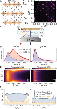
(A) Schematic crystal structure of BA2PbI4. Thin films exhibit a vertically layered morphology with repeated PbI4 monolayers separated in the z direction by BA2 spacer layers. (B) Experimental GIWAXS patterns of a spin-cast BA2PbI4 thin film. (C) Experimental geometry: Momentum- (k‖) and polarization-dependent photoluminescence (PL) spectra are collected from within the substrate by an oil-immersion 1.3–numerical aperture (NA) objective. (D) s-Polarized (left) and p-polarized (right) PL spectra of a BA2PbI4 thin film (61 nm) as collected at two very different regions in momentum space: ∣k‖∣ < 0.5k0 (solid blue) and ∣k‖∣ > k0 (dashed red). PL traces are normalized to be equivalent at 520 nm. (E) s-Polarized (left) and p-polarized (right) energy-momentum spectra from which the PL spectra of (D) were taken. The multipolar emission is readily observable in s-polarized spectra as two bright lobes at λ = 540 nm in regions with ∣k‖∣ > k0. (F) Momentum-space line cuts at 520 nm (blue) and 540 nm (orange) for s-polarization (left) and p-polarization (right). Theoretical traces (dashed lines) assuming only oriented EDs agree poorly with 540-nm s-polarized line cuts, showing that the bright high-k‖ emission cannot originate from an ED transition. a.u., arbitrary units.
Insofar as 2D HOIPs are composed of alternating semiconducting (metal halide) and insulating (organic) layers, they are recognized as “natural” quantum-well semiconductor structures (21). Accordingly, light-matter interactions in HOIPs are treated by analogy to widely studied conventional semiconductors, such as GaAs (21–24). Namely, optical transitions are assumed to be completely described by the ED approximation (3). Operating within this conventional framework, researchers have attempted to identify the origin of anomalous low-energy sideband features in 2D and 3D HOIPs, arriving at interpretations ranging from bound- or biexciton emission (21, 25) to strong phonon-carrier interactions (17, 26). Recent evidence of more “exotic” and fundamentally interesting physics, such as deep exciton self-trapping (18) and complex exciton-polaron structures (27), strong Rashba and Dresselhaus couplings (28), and an unconventional exciton fine structure (24) reflect the interplay of an unconventional electronic structure, strong spin-orbit coupling (23), structural complexity (29), and the possibility of significant dynamic symmetry-breaking mechanisms (20, 30, 31).
Energy-momentum spectroscopies have surfaced as powerful techniques for identifying anisotropic and multipolar optical phenomena in thin-film systems (7, 32–37). For example, by analyzing momentum- and polarization-dependent luminescence profiles, researchers have quantified distinct MD and ED optical transitions in lanthanide (7) and transition-metal ions (38) and have identified distinct interlayer excitons in organic semiconductor thin films (32). Here, energy-momentum spectroscopy reveals that the low-energy sideband in 2D HOIPs exhibits a peculiar polarization and angle dependence characteristic of MD radiation. While the features described herein seem to be generic to the material system, including 3D HOIPs, we exploit the highly oriented and 2D nature of BA2PbI4 (Fig. 1A) to relate the unusual radiation patterns to the underlying quantum-mechanical origins.
RESULTS
Figure 1B shows measured grazing incidence wide-angle x-ray scattering (GIWAXS) patterns from a spin-cast thin film of BA2PbI4. These data are consistent with a vertically layered structure in which PbI4 monolayers are separated by BA2 spacer layers in the out-of-plane (OP) (z) direction (39). The wavelength-dependent uniaxial complex refractive index (fig. S1) of these samples was determined by a combination of momentum-resolved reflectometry (33, 37) and variable-angle spectroscopic ellipsometry (Materials and Methods and section S1). Films exhibit a predominant in-plane (IP) optical response with weak OP dispersion, similar to high-quality single crystals (21) and consistent with the vertically layered orientation as determined from GIWAXS. By the nature of the spin-casting method, the resulting films are polycrystalline and, thus, rotationally isotropic over microscopic-length scales relevant for the measurements performed here (∼100 μm) (40). The highly oriented and rotationally invariant thin-film structure facilitates detailed analysis of momentum- and polarization-dependent optical phenomena using the experimental geometry illustrated in Fig. 1C. However, as we will describe later, the same features are observed from high-quality single crystals, and our conclusions are, thus, not restricted to spin-cast films. In energy-momentum spectroscopy, both the IP electromagnetic momentum (k‖ = <kx,ky>) and wavelength (λ) distribution of polarized reflection or luminescence are simultaneously measured by imaging the Fourier plane [i.e., back focal plane (BFP)] of a collection objective onto the entrance slit of an imaging spectrometer. Polarized spectra are acquired by placing a linear polarizer in the collection path oriented either perpendicular (s) or parallel (p) to the entrance slit (y axis). Figure 1 (D to F) show s- (left) and p-polarized (right) energy- and momentum-resolved photoluminescence (PL) measured from a 61-nm spin-cast film of BA2PbI4 at room temperature (Materials and Methods).
As seen in Fig. 1D, s-polarized PL spectra collected above the total-internal-reflection condition ∣k‖∣=∣ky∣ > k0 (dashed red) are markedly different than conventional spectra as collected by a 0.5–numerical aperture (NA) objective (∣k‖∣ ≤ 0.5k0; blue). Both s- (left) and p-polarized (right) spectra exhibit the well-established excitonic emission feature at 520 nm. However, a distinct emission feature at 540 nm (∼90-meV energy difference), apparent as a subtle shoulder at low momenta (blue), becomes the dominant emission feature at high momenta (dashed red). In contrast, this emission feature is virtually absent at all momenta in p-polarized spectra. This difference in momentum distributions is even more notable when we examine the full energy-momentum spectra (Fig. 1E; polarization orientation indicated by white arrows). The low-energy emission feature is readily observed as two bright lobes in the s-polarized spectra at ∣k‖∣ > k0. Importantly, the s-polarized emission features at 520 and 540 nm have markedly distinct curvature in k-space (Fig. 1F; left). The emission feature at 520 nm (blue) is maximal near normal (k‖ = 0) and exhibits a slow roll-off into higher momenta; the opposite is true for emission at 540 nm (orange). This illustrates the critical role of the experimental geometry on the inferred significance of this emission (fig. S2); because this light is emitted at highly oblique angles with respect to the crystal axis, it would be ordinarily be trapped (i.e., wave guided) within the high-index substrate or within the material itself, and thus only weakly collected with conventional PL geometries (e.g., blue lines in Fig. 1D). This is a general concern for 2D materials, since the polarization and directionality of the interactions are governed by highly anisotropic electronic wave functions (41). This may also have significant implications for HOIP-based LEDs; the spectrum and dynamics may be strategically enhanced or refined using photonic architectures (42).
Calculated s-polarized PL counts (section S2), assuming only the existence of ED emission, are shown in Fig. 1F (dashed lines) at both 520 nm (blue) and 540 nm (orange). Experimental PL at the 520-nm (primary exciton) emission is accurately described by the ED theory, consistent with an ED-allowed excitonic transition involving CBM and VBM states (22, 23). The 540-nm emission feature, however, is poorly modeled by the same theory. In contrast, p-polarized PL at both 520 and 540 nm are well described by ED-only theory. While low-energy emission shoulders have been observed in conventional PL spectra of both inorganic and hybrid organic-inorganic perovskites (13, 16, 18–21, 43), none of these prior works examined the polarization and momentum dependence reported here. Note that this theory completely accounts for reabsorption effects by including the complex (uniaxial) refractive index (fig. S1) of the material, thus excluding reabsorption as a possible explanation of the secondary peak. The strong high-k‖ emission excess observed predominantly in s-polarization cannot be explained by any combination of oriented ED transitions in a rotationally invariant system; a distinct ED transition centered around 540 nm would contribute with equivalent weight to both s- and p-polarized spectra, inconsistent with our data. The results presented here, thus, unambiguously demonstrate that this emission is multipolar in nature.
We observe similar multipolar features at high momenta in a number of related HOIPs (Materials and Methods and section S3), including exfoliated single crystals of the “bilayer” system BA2(CH3NH3)Pb2I7 (fig. S3), thin films of BA2PbBr4 (fig. S4), and films prepared with longer alkylammonium cations (octylammonium and dodecylammonium) (fig. S5). We find that this feature is robust to sample preparation methods and is particularly apparent in high-quality single crystals prepared with various alkylammonium cations (including phenethylammonium), and flakes mechanically exfoliated from such crystals (figs. S6 to S8). We thus conclude that this feature is general to the material system and is robust against sample preparation methods and substitutions of both the halide and spacer molecules.
While this feature is regularly observed around 540 nm in exfoliated single crystals, we note that, for similarly prepared BA2PbI4 thin films, this emission feature is observed with significantly varying strength at a range of energies between ∼30 and 90 meV below the primary emission peak. Analyses of thin-film PL spectra under varying illumination and environmental conditions (section S4 and fig. S9) suggest that this variation is due, in part, to the incorporation of oxygen or water under various processing conditions. Note, however, that prolonged illumination under ambient conditions significantly reduces the resolution of two distinct peaks, which possibly explains why this feature is so apparent in single crystals. This indicates that this sideband does not originate from atmospheric effects (e.g., water or oxygen) but rather seems to be hindered by them.
The highly s-polarized nature of the excess (i.e., non-ED) PL provides strong clues for the origins of the multipolar radiation. The candidate oriented multipoles that emit highly oblique s-polarized light are OP MDs and IP EQs (section S5 and fig. S10). Calculated 2D y-polarized radiation patterns from these multipoles are presented in Fig. 2 with s- and p-polarized k‖-space line cuts shown below and to the right of each 2D image, respectively. OP MDs (“MDz”; Fig. 2A) are associated with a circulating IP electric field and, thus, produce only s-polarized radiation. However, this s-polarized MDz contribution is functionally identical to s-polarized emission from IP EQs (Fig. 2B and section S2). Although either the MD or EQ term can be used to fit the s-polarized emission anomaly, identifying the correct multipole term is important for determining the underlying quantum mechanical origins. To this end, the OP MD and IP EQ can be distinguished by the fact that the OP MD emits no p-polarized PL; in contrast, IP EQs contribute significantly to both s- and p-polarized spectra (fig. S11). Critically, our data show virtually zero PL excess in p-polarized spectra (Fig. 1D), indicating that the multipolar PL is associated with a highly oriented OP MD transition. Note that, while the ED radiation patterns have features similar to those of the EQ, the preceding discussion is focused solely on the patterns associated with the excess counts (i.e., those not already accounted for by the ED theory). We suspect that the very subtle shoulder observed in high-k‖ p-polarized spectra is due to depolarization scattering from surface texture or slightly tilted crystallite domains in spin-cast thin films. Equivalent analyses on mechanically exfoliated single crystals (fig. S6), in which these imperfections are minimized, show no such p-polarized shoulder and confirm the MD assignment.
Fig. 2. Calculated momentum-resolved multipolar luminescence patterns at λ = 540 nm.
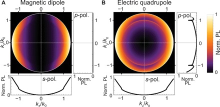
Calculated y-polarized momentum-resolved luminescence patterns from (A) an OP MD and (B) IP EQs. s-Polarized and p-polarized traces are shown below and to the right of each 2D image, respectively. Note that the radiation patterns from OP MDs and IP EQs differ along the p-polarized traces; the s-polarized traces are identical. All calculations were performed for a 61-nm film using optical constants from fig. S1.
The energy-momentum spectra, in combination with the known material optical constants (fig. S1), afford the opportunity to quantify the relative intrinsic multipolar transition rates. At each wavelength, we decompose the momentum distribution of polarized PL counts, Ns,p(λ, k‖), into a linear combination of oriented EDs and OP MDs (Materials and Methods and section S2) according to Eq. 3
| (3) |
Here, the are the normalized local density of optical states (LDOS) into which the oriented dipoles may emit, A(λ) are the wavelength-dependent intrinsic emission rates, and Cexp is a constant factor accounting for setup-specific experimental parameters. Analytical forms for the LDOS are presented in section S2. Including the MD contribution, we now see that the experimental radiation patterns for both polarizations are very well represented by the theory across all wavelengths (Fig. 3A). The resulting decomposed spectra are presented in Fig. 3B. The ED and MD peaks resolved in Fig. 3B are observed as genuinely distinct transitions. Although the MD (dashed red) contribution is notably broader than the ED (black) contribution, both exhibit similar asymmetric line shapes characteristic of luminescence from quantum wells, suggesting that the MD transition also originates from an exciton-like excited state.
Fig. 3. Multipolar decomposition of energy-momentum spectra.
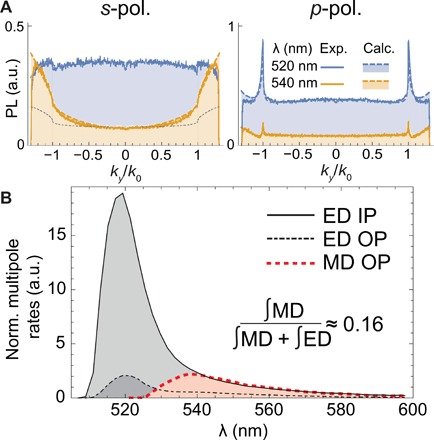
(A) Comparison of (dashed filled) theoretical and (solid) experimental momentum-space radiation profiles at λ = 520 nm (blue) and λ = 540 nm (orange) including both oriented ED and MD transitions. s-(p-)Polarized spectra are shown on the left (right). All traces show excellent agreement with theory once multipolar components are included in the theory. Calculation excluding MDs is shown as a thin gray dashed line. (B) Normalized intrinsic multipole radiation rates, CexpA(λ), determined from multipolar decompositions of energy-momentum spectra: IP EDs (solid black); OP EDs (dot-dashed black); OP MDs (dashed red).
Although multipolar emission is usually orders of magnitude weaker than ED emission, the multipolar contribution in BA2PbI4 exhibits an integrated magnitude [∫AMD(λ)dλ] comparable to that of the ED, i.e.
| (4) |
As described below, such a strong multipolar PL contribution is highly unusual and particularly unexpected when we consider the overall fast dynamics of the system. In lanthanide ions, for instance, multipolar PL is observed because of long-lived (∼100 ms) excited states associated with ED-forbidden recombination channels (2, 44). Here, however, we observe subnanosecond PL lifetimes for the main excitonic feature at 520 nm (Fig. 4A, blue circles). These PL decay traces were measured at a reduced temperature (250 K) to try to better isolate any differences in the excited-state dynamics [20] (Materials and Methods). Still, PL traces of the isolated 540-nm feature (Materials and Methods) (Fig. 4A, red squares) show no discernible differences; both traces are well represented by a biexponential decay with a primary component lifetime of τ ≈296 ps, consistent with values obtained for the primary exciton in previous reports (26, 45). Just below 250 K, BA2PbI4 shows a structural phase transition (46) accompanied by an abrupt change in the PL spectrum. Nonetheless, distinct ED and MD PL features can be identified at low temperatures by comparing spectra from highly oriented and randomly oriented film morphologies (e.g., fig. S14), further supporting the generality of MD emission over a large temperature range. These two emission features also show nearly identical behavior under intensity-dependent PL. Throughout a very broad range of excitation intensities (Iexc = 1 to 750 mW/cm2), the spectral shape is observed to be nearly invariant (Fig. 4B, darker colored lines). Only at extremely high excitation intensities (Iexc > 103 mW/cm2; lighter colored lines) does the spectrum begin to vary, with the low-energy feature growing in relative strength. Power-law fits of the decomposed spectra (Fig. 4C) reveal that both the ED contribution (black; αED=1.17± 0.05) and the multipolar contribution (red; αMD = 1.15±0.04) grow in parallel. Note that the data presented in Fig. 4 were measured from polycrystalline samples with random crystallite orientations to enhance the visibility of the 540-nm emission feature with conventional spectroscopy techniques (Materials and Methods), but similar conclusions are made from analogous measurements on spin-cast thin films (section S6 and fig. S12). This intensity dependence excludes biexcitons (α = 2) or excitons bound to extrinsic defects (α <1) as a likely origin. In light of recent reports highlighting the prevalence of low-energy “white-light emitting” states in 2D HOIPs (18), we note that this pump dependence is consistent with an (intrinsic) self-trapping mechanism, but the 90-meV energy difference observed here is significantly smaller than that of previously observed white light–emitting states (vida infra).
Fig. 4. Dynamics and pump dependence of emission features.
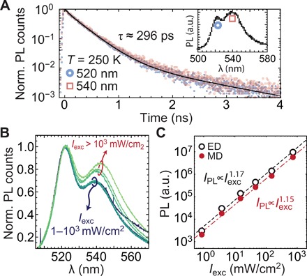
(A) Time-resolved PL traces of the 520-nm (blue) and 540-nm (red) emission features from drop-cast films at 250 K (Materials and Methods). Data at both wavelengths are well represented by a biexponential decay (black) with a τ = 296 ps primary component. The reduced temperature of 250 K was chosen to reduce thermally assisted energy transfer between states. (B) Pump intensity dependence of PL spectra from a drop-cast film (Materials and Methods) at T ≈ 300 K. Data have been normalized to the PL at 520 nm. (C) Log-log plot of integrated PL strength [IPL=∫A(λ)dλ] from ED (black) and MD (brown) contributions as a function of excitation intensity, Iexc. Lines are power law fits: with nearly identical exponents for the ED (α = 1.17 ± 0.05; black) and MD (α = 1.15 ± 0.04; red) emission.
The absolute radiative lifetimes can be estimated from the measured PL lifetime, quantum yield (PLQY), and normalized multipolar emission rates. Assuming that the measured PLQY of 0.4% (Materials and Methods) is representative of both emission features, our data imply radiative rates of 1.4×10⁷ s−1 and 1.9×10⁶ s−1 for the ED and MD, respectively, assuming that the emission arises from identical exciton densities. [Note that this PLQY is comparable to previously reported values for this material (16).] However, considering the 90-meV energy splitting, the observed low-energy (MD) transition rate could be enhanced relative to the high-energy (ED) transition because of the thermal occupation of excited states. If we assume two distinct emissive channels in thermal equilibrium, the intrinsic MD radiative rate is reduced by a factor of exp(90 meV/26 meV)≈30, yielding an intrinsic radiative rate of 6.0×10⁴ s−1. Even with this more conservative estimate, the inferred multipolar radiative rate is three orders of magnitude larger than any MD emission rate reported from atomic systems (2) and is curiously close to that predicted from the discussion surrounding (Eqs. 1 and 2). There is, to our knowledge, no crystalline system to which this may yet be compared. The multipolar emission observed in BA2PbI4 is extraordinarily bright and challenges conventional understanding of multipolar light-matter interactions.
We now consider the electronic band structure as it relates to the origins of the multipolar PL signature. Density functional theory (DFT) calculations (Materials and Methods) of the BA2PbI4 electronic structure are summarized in Fig. 5. At each wave vector, k, along the Γ-X and Γ-U directions of the reciprocal lattice, we project the ground-state eigenfunctions onto a basis consisting of I (Fig. 5B) and Pb (Fig. 5C) orbitals with symmetries corresponding to s, px, py, and pz orbitals. The weight of the projection is represented by the size of the circle at each k. The VBM (set to 0 eV in the band diagrams) comprises roughly equal contributions from I (5)p orbitals and Pb (6)s orbitals, in agreement with previous reports (23). (I and Pb py contributions are not shown since they are nearly identical to px, because of the system’s approximate C4 symmetry.) Note, however, that the I pz contribution is significantly suppressed relative to the IP contributions. The CBM comprises nearly equal contributions of Pb (6)px and (6)py orbitals with an absent pz contribution. (See fig. S13 for the complete set of band character projections and charge density plots.) The symmetries of the CBM and VBM states participating in optical transitions, however, are governed by the bonding character of the constituent atoms. Previous studies have assigned (p-like) and (s-like) symmetries to the CBM and VBM wave functions, ∣ψCBM〉 and ∣ψVBM〉, respectively (22, 23). In analogy with conventional semiconductors, these states may be qualitatively represented by ∣X〉 and ∣Y〉 (CBM), and ∣S〉 (VBM); a predominantly IP ED transition is described by a symmetry analysis of the ED matrix elements between CBM and VBM states: 〈S∣x∣X〉 ≈ 〈S∣y∣Y〉 ≠ 0 and 〈S∣z∣ψCBM〉 ≈ 0 (23). The nonzero EDz contribution observed here and in previous experiments (21, 36, 37) likely arises from a non-negligible I pz contribution at the VBM and an I (5)s contribution at the CBM (fig. S13). Electron-hole correlations yield three distinct (1s) exciton levels with odd parity, corresponding to the direct product of , and an even parity crystal ground state (22). However, selection rules still reflect the underlying VBM and CBM states, and these conclusions are, thus, unaltered. These treatments have been used with apparent success to describe the low-temperature exciton spectrum observed in previous reports (21, 22, 24).
Fig. 5. Calculated band structure and band character of BA2PbI4.
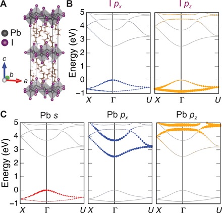
(A) The BA2PbI4 unit cell used in DFT calculations comprises two distinct layers. Pb atoms are shown in black, and I atoms are shown in purple. (B and C) Computed band structures along the Γ-X and Γ-U directions of the reciprocal lattice, projected onto Pb and I orbitals with symmetries of s, px, py, and pz. The relative weights are represented by the size of the circles at each momentum. (B) I px (left) and pz (right) contributions to the band structure. I (5)p orbitals contribute primarily to the valence bands. The VBM (energy set to 0 eV) predominantly derives from IP I (5)p orbitals (px and py). (C) Pb s (left), px (center), and pz (right) contributions to the band structure. The CBM predominantly derives from IP Pb (6)p orbitals (px and py). The VBM also shows significant contributions from Pb (6)s orbitals. In all cases, py contributions are identical to px contributions and are, thus, not shown.
In contrast to the ED term, the MD term connects states with equivalent parity (44, 47). Symmetry-based analyses of multipolar matrix elements are outlined in section S8. Qualitatively, in the electron-electron picture, MDz connects CBM and VBM states with IP extended orbitals; the necessary Bloch states are absent in the VBM, and thus, these multipolar transitions are strictly forbidden within the aforementioned treatment for 1s excitons (eq. S44). While this selection rule is reversed for a p-like exciton envelope function (eq. S48), the hydrogenic 2p exciton state lies at energies ≈300 meV higher than the 1s exciton state (22) and is, thus, excluded as a likely candidate. Our experimental results, thus, suggest the presence of structural distortions that generate a low-energy excited state (e.g., exciton or exciton-polaron) with distinct (i.e., even) parity. A surge of recent reports highlight the importance of dynamic symmetry–breaking mechanisms, e.g., thermally induced lattice distortions (20, 28, 30, 31) and a strong polaronic character of excited states (27, 48–50), both reflecting the relatively “soft” ionic lattice. Although numerous DFT studies have explored the role of typical static asymmetries (29) and thermal fluctuations in HOIPs (31), none have established a significant change in electronic state symmetries or optical selection rules. The MD feature observed here appears as a spectrally distinct excited state, favoring polaronic effects—namely, exciton self-trapping—as a potential origin, especially in light of potential parity-breaking polaron phenomena (49–51). For example, a p-like electron-hole configuration with lower energy—the “off-site” self-trapped exciton in some references—may be induced and stabilized by interactions with antisymmetric lattice distortions (50, 51). The pump dependence (Fig. 4C) is consistent with a self-trapping mechanism. This hypothesis is bolstered by a marked thermal red shift of the MD feature (fig. S14), mirroring similar thermal shifts observed for self-trapped exciton-polaron states in lithium niobate due to significant “lattice softening” with increasing temperatures (52).
DISCUSSION
Exploiting the highly oriented structure of 2D HOIPs, and taking into account polarization-, wavelength-, and angle-dependent collection effects, we identify an oriented, exceptionally fast MD optical transition that appears as a PL sideband at room temperature. The unconventional radiation properties of the sideband luminescence have not yet been acknowledged. Consequently, the magnitude of these transitions has been largely underestimated. Similar directional effects are expected to afflict optical studies of other 2D materials (41). The presence of a multipolar transition in 2D HOIPs is evidently inherent to the material system. Accounting for extrinsic collection effects, we show that the MD radiative rate is at least three orders of magnitude larger than multipolar emission rates previously identified in atomic systems; there is yet no other crystalline system to which these rates may be compared.
This observation of bright MD luminescence, coupled with first-principles considerations of radiation rates (Eqs. 1 and 2), suggests that multipolar phenomena may be more prevalent than previously thought and challenges a long-standing assumption that may limit further understanding and development of new materials, especially for optoelectronic devices such as LEDs and lasers. Although the precise role of spin-orbit coupling and quantum confinement remains unresolved, the physics demonstrated here may affect the development of quantum information applications based on “dark” (ED-forbidden) excitons in 2D materials (53). Metamaterial communities regularly exploit classical electric dipolar and multipolar resonances (4, 54) to engineer directional radiation patterns, but assume that multipolar effects are negligible at the quantum level. The distinct electric field symmetries associated with the spectrally separated ED and MD radiation in 2D HOIPs thus point toward the possibility of engineering unique light-matter interactions in nanoscale resonators constructed from 2D HOIPs, as has recently been explored in WSe2 (55).
MATERIALS AND METHODS
Samples
Solutions of (C4H9NH3)2PbI4 were prepared according to the procedures described in (40) to concentrations of 150 mg/ml in an N2-filled glovebox. Thin films were dynamically spin cast (solution deposited while spinning) in an N2-filled glovebox on 0.180-mm fused silica substrates at 8000 rpm for 60 s and subsequently thermally annealed at 70°C for 30 min, producing films with thicknesses of ∼61 nm. Film thicknesses were measured with atomic force microscopy (AFM) (Asylum MFP-3D) in tapping mode using a tip-scratch method and measuring over the resulting groove. For variable angle spectroscopic ellipsometry studies, thin films were prepared identically, upon Si substrates. All samples were kept in a nitrogen-vacated dry box immediately following film preparation until the time of optical measurements. Single crystals of A2PbI4, with A = butylammonium, octylammonium, and dodecylammonium, were grown in an N2-filled glovebox according to the methods described in (56). Single crystals of (C4H9NH3)2(CH3NH3)n−1PbnI3n + 1 with n = 2 (fig. S3) were grown according to the procedures described in (10). Mechanically exfoliated flakes (figs. S5 to S7) were produced by the “Scotch tape method”. Flakes were identified visually by means of an inverted microscope with magnification varying from ×10 to ×100. Flake thicknesses were determined by AFM in a tapping mode after optical measurements were made. Thin films of (C4H9NH3)2PbBr4 (butylammonium lead bromide; fig. S6) were prepared from (C4H9NH3)2PbI4 thin films by a vapor exchange method according to procedures specified in section S3. Thin films of (C8H17NH3)2PbI4 (octylammonium lead iodide) and (C12H25NH3)2PbI4 (dodecylammonium lead iodide) (fig. S7) were prepared according to the procedures described above with the substitution of butylammonium for octylammonium and dodecylammonium, respectively. For time-resolved PL and pump power dependence studies (Fig. 4), samples were prepared by drop casting directly on substrates, which strategically produced thick films with mixed crystallite orientations and significant scattering texture by minimizing wetting of the substrate, thereby enhancing the visibility of the 540-nm emission without the use of high-NA imaging techniques.
Grazing incidence wide-angle x-ray scattering
GIWAXS experiments were conducted at the Advanced Light Source at beamline 7.3.3. The energy of the incident beam was at 10 keV, and a Pilatus 2M area detector was used. The x-ray scattering data were taken at incidence angle of 0.3°, and samples were kept in a helium environment during x-ray exposure to minimize air scattering and sample degradation. The collected images were processed using GIXSGUI (57), and the beam center and the sample-to-detector distance were calibrated using silver behenate (AgBe).
Optical constants
Complex uniaxial optical constants for thin films of (C4H9NH3)2PbI4 were determined by a combination of momentum-resolved reflectometry and variable-angle spectroscopic ellipsometry according to the procedures detailed in (33, 37). The results are presented in section S1.
Energy-momentum spectroscopy
Thin film samples were illuminated by a 405-nm LED (ThorLabs M405 L3). The incident light was filtered by a 405-nm short-pass filter and reflected by a 415-nm dichroic mirror to remove overlap with the emission wavelengths. The emitted PL was transmitted through the same dichroic as well as a 417-nm long-pass filter. The energy and y-momentum, ky, of the light was then measured by imaging the objective (Nikon CFI Plan Fluor 100× Oil, 1.3 NA) BFP to the entrance slit of an imaging spectrometer (Princeton Instruments IsoPlane SCT320 with Princeton Instruments PIXIS 1024BRX). An analyzing polarizer was applied to the image such that light along the ky axis was either p-polarized (vertical polarizer alignment) or s-polarized (horizontal polarizer alignment). For the data presented in Figs. 1 and 3, measurements were performed in ambient conditions with illumination intensities below ∼1 mW/cm2. The exposed films showed no visible signs of photodegradation. The resulting energy-momentum spectra were decomposed into various multipolar contributions using methods described elsewhere (7, 32), assuming a uniform distribution of dipole/multipole locations along the z axis. Film thicknesses were taken from AFM (see the “Samples” section). Film optical constants were determined from the same films using methods described completely in section S1. For photodegradation studies (fig. S11), measurements were performed in both ambient and inert (N2) conditions, and illumination intensities were swept between ∼5 and 100 mW/cm2. No visible signs of photodegradation were observed for samples exposed in inert conditions. Integration times for all measurements were on the order of 10 to 1000 s, depending on illumination intensity. For energy-momentum spectroscopy of exfoliated flakes, after sample preparation (see the “Samples” section), a heavy flow of nitrogen gas was applied to the sample. The nitrogen flow persisted for the duration of the optical measurements. Single crystals and platelets were identified by eye under a 100× oil immersion objective. Exfoliated crystals were illuminated by focusing a 405-nm fiber-coupled laser to the image plane at the rear entrance of the microscope. At the level of the sample, the focused spot had a width of ∼5 μm. Total illumination intensities were kept below ∼60 mW/cm2. Integration times were on the order of 100 to 1000 s. The exposed crystals showed no significant signs of optical degradation. All energy-momentum spectroscopy measurements and pump-dependent PL measurements were performed at room temperature.
Time-resolved photoluminescence
Time-correlated single-photon counting measurements (Fig. 4A) were performed at the University of California, Santa Barbara (UCSB) Optical Characterization Facility. Approximately 100-fs excitation pulses with a wavelength of 400 nm were generated by doubling the fundamental frequency of a femtosecond Ti:sapphire laser (Spectra-Physics Tsunami) pulses in a commercial optical harmonic generator (Inrad). The laser repetition rate was reduced to 2 MHz by a home-made acousto-optical pulse picker to avoid saturation of the chromophore. The system is equipped with a thermoelectrically cooled single-photon counting avalanche photodiode (Micro Photon Devices) and electronics board (Becker & Hickl SPC-630) and has an instrument response time of 30 ps. The fluorescence signal was dispersed in an Acton Research SPC-500 monochromator after passing through a long-pass filter to remove the pump wavelength. In addition to the time-resolved detector, the monochromator is equipped with a charge-coupled device camera (Roper Scientific PIXIS-400), allowing for monitoring of the time-averaged fluorescence spectrum. To maximize the 540-nm PL signal, films were produced by the drop-casting method as described in the “Samples” section. Samples were mounted within an evacuated cryostat at 250 K maintained at ∼0.5×10⁻⁵ mbar to avoid photodegradation. Samples were pumped at 400 nm with ≈0.025 μJ/cm2 per pulse with a 2-MHz repetition rate. PL was collected in a reflection geometry with the pump and collection optics at 90° with respect to each other and approximately 45° with respect to the sample normal. The data shown in Fig. 4A were acquired at 250 K to minimize thermally assisted excitation transfer between the states. Analogous measurements presented in the Supplementary Materials were performed on spin-cast thin films at room temperature by collecting the PL at high angles (with respect to the sample interfaces) through a linear polarizer in an s-polarized configuration.
Pump-dependent photoluminescence
For pump power dependence studies as presented in Fig. 4, B and C, films were prepared according to the drop-casting method as described in the “Samples” section. Regions with reoriented crystals or sufficient scattering texture were identified visually. The reorientation and/or scattering texture allowed the 540-nm emission to be detected with a 10× 0.3 NA (Nikon CFI Plan Fluor). Samples were illuminated by a loosely focused spot (∼100- μm beam waste) in inert (N2) conditions according to the methods described for single crystals above. Illumination intensities were swept between ∼1 mW/cm2 and 1 W/cm2. No signs of photodegradation were observed for pump powers below ∼750 mW/cm2. Integration times for all measurements were on the order of 0.1 to 250 s, depending on illumination intensity. Spectra were decomposed to a sum of two (asymmetric) Gaussian distributions with stretched tails and fixed widths. The centers of the distributions were held at 522 and 541 nm. Only the amplitudes of the two components were fit at each illumination intensity. Measurements were performed at room temperature.
PL lifetime, quantum yield
PLQY of spin-cast thin films was measured using a Horiba spectrometer (FluoroMax 4) and integrating sphere (Horiba Quanta-φ) with 400-nm wavelength excitation. To improve PL counts, samples were spin cast at 1500 rpm, resulting in films of ∼300-nm thickness. The photon absorption rate was determined by scanning over the excitation line of the attenuated beam (nominal optical density = 3, measured area fill correction of 803) with the sample in place and comparing to a nonabsorbing reference (blank quartz substrate). A 405-nm short-pass filter (Semrock) was in place during excitation and emission measurements, and a 405-nm long-pass filter (Semrock) was in place for emission measurements only. A 1% correction factor was applied to account for long-pass transmission efficiencies. We note that the 540-nm emission was clearly visible in integrating sphere PL measurements, as expected since PL was collected over all angles. Measurements were performed at room temperature.
Band structure
First-principles calculations were performed on the basis of DFT as implemented in the Vienna Ab initio Simulation Package (VASP) (58). We used projector-augmented wave (PAW) (59) pseudopotentials with a plane-wave energy cutoff of 500 eV. A Γ-centered 3 × 3 × 1 k-point grid was used for sampling the first Brillouin zone. The Heyd-Scuseria-Ernzerhof (HSE) (60) hybrid functional was used for the exchange-correlation interactions. A mixing parameter of 0.45 was used for the HSE functional including spin-orbit coupling to give a consistent bandgap with experiment. The atomic positions and lattice constants were fully relaxed; the optimized lattice constants were 8.79, 8.80, and 29.07 Å, respectively.
Supplementary Material
Acknowledgments
We thank C. G. Van de Walle, M. E. Flatte, H. I. Karunadasa, and M. G. Kanatzidis for the insightful discussions. Funding: Energy-momentum spectroscopy measurements and analyses were supported by the National Science Foundation (DMR-1454260 and OIA-1538893) and by the Air Force Office of Scientific Research (grant no. FA9550-16-1-0393). Time- and intensity-resolved optical measurements and analyses, as well as studies of exfoliated single crystals comprising varying organic spacers were supported as part of Quantum Materials for Energy Efficient Neuromorphic Computing, an Energy Frontier Research Center funded by the U.S. Department of Energy (DOE), Office of Science, Basic Energy Sciences (BES), under award # DE-SC0019273. Materials synthesis and structural characterization were supported by the U.S. DOE, Office of Science, BES, under award DE-SC-0012541. PLQY measurements were performed at the MRL Shared Experimental Facilities, supported by the MRSEC Program of the NSF under award no. DMR 1720256, a member of the NSF-funded Materials Research Facilities Network (www.mrfn.org). Portions of the work were performed at the Advanced Light Source, supported by the Director, Office of Science, Office of BES, of the U.S. DOE under contract no. DEAC02-05CH11231. A portion of this work was performed in the UCSB Nanofabrication Facility. The research reported here also made use of the shared facilities of the UCSB MRSEC (National Science Foundation DMR 1720256), a member of the Materials Research Facilities Network (www.mrfn.org). R.M.K. gratefully acknowledges the National Defense Science and Engineering Graduate fellowship for financial support. X.Z. was supported by the U.S. DOE, Office of Science, BES under award no. DE-SC0010689. Computational resources were provided by the National Energy Research Scientific Computing Center, a DOE Office of Science User Facility supported by the Office of Science of the U.S. DOE under contract no. DE-AC02-05CH11231. Author contributions: R.A.D., M.L.C., and J.A.S. conceived the experiment. R.A.D., W.L., and X.D. performed optical measurements. R.A.D. performed electromagnetic calculations and analyzed the optical data with R.Z. and J.A.S. R.A.D., N.R.V., C.J.D., and R.M.K. synthesized the samples. N.R.V., C.J.D., and R.M.K. performed and analyzed the GIWAXS measurements with M.L.C. X.Z. performed numerical band structure calculations. R.A.D. developed the quantum mechanical and group theory calculations. J.A.S. supervised the project. All authors discussed the results and commented on the manuscript. Competing interests: All authors declare that they have no competing interests. Data and materials availability: All data needed to evaluate the conclusions in the paper are present in the paper and/or the Supplementary Materials. Additional data related to this paper may be requested from the authors.
SUPPLEMENTARY MATERIALS
Supplementary material for this article is available at http://advances.sciencemag.org/cgi/content/full/6/6/eaay4900/DC1
Section S1. Optical constants of (C4H9NH3)2PbI4 thin films
Section S2. Calculating normalized intrinsic multipolar emission rates
Section S3. Polarization-dependent shoulder emission in related layered lead-halide perovskites
Section S4. Photodegradation effects on the multipolar emission energy
Section S5. Radiation patterns from oriented multipoles
Section S6. TRPL and pump power dependence of multipolar decomposition in thin films
Section S7. Temperature dependence of multipolar PL in 2D HOIPs
Section S8. Matrix elements of multipolar transitions
Fig. S1. Complex uniaxial refractive index of BA2PbI4.
Fig. S2. Impact of experimental geometry on measured PL.
Fig. S3. Multipolar emission in exfoliated single crystals of BA2MAn−1PbnI3n+1 with n = 1 to 2.
Fig. S4. Multipolar emission in butylammonium lead bromide.
Fig. S5. Polarization-dependent PL in various alkylammonium-PbI4 spin-cast thin films.
Fig. S6. Summarized analysis of exfoliated single crystals of BA2PbI4.
Fig. S7. Summarized analysis of exfoliated single crystals of OA2PbI4.
Fig. S8. Summarized analysis of exfoliated single crystals of DDA2PbI4.
Fig. S9. Illumination intensity- and environment-dependent evolution of EQ emission in thin films of BA2PbI4.
Fig. S10. BFP radiation patterns from oriented multipoles.
Fig. S11. BFP radiation patterns from IP EQs.
Fig. S12. TRPL and pump power dependence of multipolar decomposition in spin-cast thin films of BA2PbI4.
Fig. S13. Calculated band structure, character, and charge densities.
Fig. S14. Temperature-dependent PL of ED and MD emission features in 2D HOIPs.
REFERENCES AND NOTES
- 1.R. Cowan, The Theory of Atomic Structure and Spectra (University of California Press, 1981). [Google Scholar]
- 2.Dodson C. M., Zia R., Magnetic dipole and electric quadrupole transitions in the trivalent lanthanide series: Calculated emission rates and oscillator strengths. Phys. Rev. B 86, 125102 (2012). [Google Scholar]
- 3.G. Bastard, Wave Mechanics Applied to Semiconductor Heterostructures (Les Éditions de Physique, 1988). [Google Scholar]
- 4.Shalaev V. M., Optical negative-index metamaterials. Nat. Photonics 1, 41–48 (2007). [Google Scholar]
- 5.Andersen M. L., Stobbe S., Srensen A. S., Lodahl P., Strongly modified plasmon-matter interaction with mesoscopic quantum emitters. Nat. Phys. 7, 215–218 (2011). [Google Scholar]
- 6.Vaskin A., Mashhadi S., Steinert M., Chong K. E., Keene D., Nanz S., Abass A., Rusak E., Choi D.-Y., Fernandez-Corbaton I., Pertsch T., Rockstuhl C., Noginov M. A., Kivshar Y. S., Neshev D. N., Noginova N., Staude I., Manipulation of magnetic dipole emission from Eu3+ with Mie-resonant dielectric metasurfaces. Nano Lett. 19, 1015–1022 (2019). [DOI] [PubMed] [Google Scholar]
- 7.Taminiau T. H., Karaveli S., van Hulst N. F., Zia R., Quantifying the magnetic nature of light emission. Nat. Commun. 3, 979 (2012). [DOI] [PubMed] [Google Scholar]
- 8.Brenner T. M., Egger D. A., Kronik L., Hodes G., Cahen D., Hybrid organic-inorganic perovskites: Low-cost semiconductors with intriguing charge-transport properties. Nat. Rev. Mater. 1, 15007 (2016). [Google Scholar]
- 9.Pedesseau L., Sapori D., Traore B., Robles R., Fang H.-H., Loi M. A., Tsai H., Nie W., Blancon J.-C., Neukirch A., Tretiak S., Mohite A. D., Katan C., Even J., Kepenekian M., Advances and promises of layered halide hybrid perovskite semiconductors. ACS Nano 10, 9776–9786 (2016). [DOI] [PubMed] [Google Scholar]
- 10.Stoumpos C. C., Cao D. H., Clark D. J., Young J., Rondinelli J. M., Jang J. I., Hupp J. T., Kanatzidis M. G., Ruddlesden-Popper hybrid lead iodide perovskite 2D homologous semiconductors. Chem. Mater. 28, 2852–2867 (2016). [Google Scholar]
- 11.Kamminga M. E., Fang H.-H., Filip M. R., Giustino F., Baas J., Blake G. R., Loi M. A., Palstra T. T. M., Confinement effects in low-dimensional lead iodide perovskite hybrids. Chem. Mater. 28, 4554–4562 (2016). [Google Scholar]
- 12.Congreve D. N., Weidman M. C., Seitz M., Paritmongkol W., Dahod N. S., Tisdale W. A., Tunable light-emitting diodes utilizing quantum-confined layered perovskite emitters. ACS Photonics 4, 476–481 (2017). [Google Scholar]
- 13.Tsai H., Nie W., Blancon J.-C., Stoumpos C. C., Soe C. M. M., Yoo J., Crochet J., Tretiak S., Even J., Sadhanala A., Azzellino G., Brenes R., Ajayan P. M., Bulovi V., Stranks S. D., Friend R. H., Kanatzidis M. G., Mohite A. D., Stable light-emitting diodes using phase-pure Ruddlesden-Popper layered perovskites. Adv. Mater. 30, 1704217 (2018). [DOI] [PubMed] [Google Scholar]
- 14.Yang X., Zhang X., Deng J., Chu Z., Jiang Q., Meng J., Wang P., Zhang L., Yin Z., You J., Efficient green light-emitting diodes based on quasi-two-dimensional composition and phase engineered perovskite with surface passivation. Nat. Commun. 9, 570 (2018). [DOI] [PMC free article] [PubMed] [Google Scholar]
- 15.Raghavan C. M., Chen T.-P., Li S.-S., Chen W.-L., Lo C.-Y., Liao Y.-M., Haider G., Lin C.-C., Chen C.-C., Sankar R., Chang Y.-M., Chou F.-C., Chen C.-W., Low-threshold lasing from 2D homologous organic-inorganic hybrid Ruddlesden-Popper perovskite single crystals. Nano Lett. 18, 3221–3228 (2018). [DOI] [PubMed] [Google Scholar]
- 16.Mitzi D. B., Synthesis, crystal structure, and optical and thermal properties of (C4H9NH3)2MI4 (M = Ge, Sn, Pb). Chem. Mater. 8, 791–800 (1996). [Google Scholar]
- 17.Gauthron K., Lauret J.-S., Doyennette L., Lanty G., Choueiry A. A., Zhang S. J., Brehier A., Largeau L., Mauguin O., Bloch J., Deleporte E., Optical spectroscopy of two-dimensional layered (C6H5C2H4-NH3)2-PbI4 perovskite. Opt. Express 18, 5912–5919 (2010). [DOI] [PubMed] [Google Scholar]
- 18.Smith M. D., Karunadasa H. I., White-Light Emission from Layered Halide Perovskites. Acc. Chem. Res. 51, 619–627 (2018). [DOI] [PubMed] [Google Scholar]
- 19.Blancon J.-C., Stier A. V., Tsai H., Nie W., Stoumpos C. C., Traor B., Pedesseau L., Kepenekian M., Katsutani F., Noe G. T., Kono J., Tretiak S., Crooker S. A., Katan C., Kanatzidis M. G., Crochet J. J., Even J., Mohite A. D., Scaling law for excitons in 2D perovskite quantum wells. Nat. Commun. 9, 2254 (2018). [DOI] [PMC free article] [PubMed] [Google Scholar]
- 20.Wu B., Yuan H., Xu Q., Steele J. A., Giovanni D., Puech P., Fu J., Ng Y. F., Jamaludin N. F., Solanki A., Mhaisalkar S., Mathews N., Roeffaers M. B. J., Grätzel M., Hofkens J., Sum T. C., Indirect tail states formation by thermal-induced polar fluctuations in halide perovskites. Nat. Commun. 10, 484 (2019). [DOI] [PMC free article] [PubMed] [Google Scholar]
- 21.Ishihara T., Takahashi J., Goto T., Optical properties due to electronic transitions in two-dimensional semiconductors (CnH2n+1NH3)2PbI4. Phys. Rev. B 42, 11099–11107 (1990). [DOI] [PubMed] [Google Scholar]
- 22.Tanaka K., Takahashi T., Kondo T., Umeda K., Ema K., Umebayashi T., Asai K., Uchida K., Miura N., Electronic and excitonic structures of inorganic-organic perovskite-type quantum-well crystal (C4H9NH3)2PbBr4. Jpn. J. Appl. Phys. 44, 5923 (2005). [Google Scholar]
- 23.Even J., Pedesseau L., Dupertuis M.-A., Jancu J.-M., Katan C., Electronic model for self-assembled hybrid organic/perovskite semiconductors: Reverse band edge electronic states ordering and spin-orbit coupling. Phys. Rev. B 86, 205301 (2012). [Google Scholar]
- 24.Becker M. A., Vaxenburg R., Nedelcu G., Sercel P. C., Shabaev A., Mehl M. J., Michopoulos J. G., Lambrakos S. G., Bernstein N., Lyons J. L., Stferle T., Mahrt R. F., Kovalenko M. V., Norris D. J., Rain G., Efros A. L., Bright triplet excitons in caesium lead halide perovskites. Nature 553, 189–193 (2018). [DOI] [PubMed] [Google Scholar]
- 25.Chong W. K., Thirumal K., Giovanni D., Goh T. W., Liu X., Mathews N., Mhaisalkar S., Sum T. C., Dominant factors limiting the optical gain in layered two-dimensional halide perovskite thin films. Phys. Chem. Chem. Phys. 18, 14701–14708 (2016). [DOI] [PubMed] [Google Scholar]
- 26.Straus D. B., Hurtado Parra S., Iotov N., Gebhardt J., Rappe A. M., Subotnik J. E., Kikkawa J. M., Kagan C. R., Direct observation of electron-phonon coupling and slow vibrational relaxation in organic-inorganic hybrid perovskites. J. Am. Chem. Soc. 138, 13798–13801 (2016). [DOI] [PubMed] [Google Scholar]
- 27.Neutzner S., Thouin F., Cortecchia D., Petrozza A., Silva C., Srimath Kandada A. R., Exciton-polaron spectral structures in two-dimensional hybrid lead-halide perovskites. Phys. Rev. Mater. 2, 064605 (2018). [Google Scholar]
- 28.Kepenekian M., Even J., Rashba and Dresselhaus couplings in halide perovskites: Accomplishments and opportunities for spintronics and spin-orbitronics. J. Phys. Chem. Lett. 8, 3362–3370 (2017). [DOI] [PubMed] [Google Scholar]
- 29.Zhang X., Shen J.-X., Wang W., Van de Walle C. G., First-principles analysis of radiative recombination in lead-halide perovskites. ACS Energy Lett. 3, 2329–2334 (2018). [Google Scholar]
- 30.Niesner D., Hauck M., Shrestha S., Levchuk I., Matt G. J., Osvet A., Batentschuk M., Brabec C., Weber H. B., Fauster T., Structural fluctuations cause spin-split states in tetragonal (CH3NH3)PbI3 as evidenced by the circular photogalvanic effect. Proc. Natl. Acad. Sci. U.S.A. 115, 9509–9514 (2018). [DOI] [PMC free article] [PubMed] [Google Scholar]
- 31.Zheng C., Yu S., Rubel O., Structural dynamics in hybrid halide perovskites: Bulk Rashba splitting, spin texture, and carrier localization. Phys. Rev. Mater. 2, 114604 (2018). [Google Scholar]
- 32.Schuller J. A., Karaveli S., Schiros T., He K., Yang S., Kymissis I., Shan J., Zia R., Orientation of luminescent excitons in layered nanomaterials. Nat. Nanotechnol. 8, 271–276 (2013). [DOI] [PubMed] [Google Scholar]
- 33.DeCrescent R. A., Brown S. J., Schlitz R. A., Chabinyc M. L., Schuller J. A., Model-blind characterization of thin-film optical constants with momentum-resolved reflectometry. Opt. Express 24, 28842–28857 (2016). [DOI] [PubMed] [Google Scholar]
- 34.Brown S. J., DeCrescent R. A., Nakazono D. M., Willenson S. H., Ran N. A., Liu X., Bazan G. C., Nguyen T.-Q., Schuller J. A., Enhancing organic semiconductor-surface plasmon polariton coupling with molecular orientation. Nano Lett. 17, 6151–6156 (2017). [DOI] [PubMed] [Google Scholar]
- 35.Scott R., Heckmann J., Prudnikau A. V., Antanovich A., Mikhailov A., Owschimikow N., Artemyev M., Climente J. I., Woggon U., Grosse N. B., Achtstein A. W., Directed emission of CdSe nanoplatelets originating from strongly anisotropic 2D electronic structure. Nat. Nanotechnol. 12, 1155–1160 (2017). [DOI] [PubMed] [Google Scholar]
- 36.Fieramosca A., De Marco L., Passoni M., Polimeno L., Rizzo A., Rosa B. L. T., Cruciani G., Dominici L., De Giorgi M., Gigli G., Andreani L. C., Gerace D., Ballarini D., Sanvitto D., Tunable out-of-plane excitons in 2D single-crystal perovskites. ACS Photonics 5, 4179–4185 (2018). [Google Scholar]
- 37.DeCrescent R. A., Venkatesan N. R., Dahlman C. J., Kennard R. M., Chabinyc M. L., Schuller J. A., Optical constants and effective-medium origins of large optical anisotropies in layered hybrid organic/inorganic perovskites. ACS Nano 13, 10745–10753 (2019). [DOI] [PubMed] [Google Scholar]
- 38.Karaveli S., Wang S., Xiao G., Zia R., Time-resolved energy-momentum spectroscopy of electric and magnetic dipole transitions in Cr3+:MgO. ACS Nano 7, 7165–7172 (2013). [DOI] [PubMed] [Google Scholar]
- 39.Venkatesan N. R., Kennard R. M., DeCrescent R. A., Nakayama H., Dahlman C. J., Perry E. E., Schuller J. A., Chabinyc M. L., Phase intergrowth and structural defects in organic metal halide Ruddlesden-Popper thin films. Chem. Mater. 30, 8615–8623 (2018). [Google Scholar]
- 40.Venkatesan N. R., Labram J. G., Chabinyc M. L., Charge-carrier dynamics and crystalline texture of layered Ruddlesden-Popper hybrid lead iodide perovskite thin films. ACS Energy Lett. 3, 380–386 (2018). [Google Scholar]
- 41.Wang G., Robert C., Glazov M., Cadiz F., Courtade E., Amand T., Lagarde D., Taniguchi T., Watanabe K., Urbaszek B., Marie X., In-plane propagation of light in transition metal dichalcogenide monolayers: Optical selection rules. Phys. Rev. Lett. 119, 047401 (2017). [DOI] [PubMed] [Google Scholar]
- 42.Cueff S., Li D., Zhou Y., Wong F. J., Kurvits J. A., Ramanathan S., Zia R., Dynamic control of light emission faster than the lifetime limit using VO2 phase-change. Nat. Commun. 6, 8636 (2015). [DOI] [PMC free article] [PubMed] [Google Scholar]
- 43.Iaru C. M., Geuchies J. J., Koenraad P. M., Vanmaekelbergh D., Silov A. Y., Strong carrier-phonon coupling in lead halide perovskite nanocrystals. ACS Nano 11, 11024–11030 (2017). [DOI] [PMC free article] [PubMed] [Google Scholar]
- 44.S. Sugano, Y. Tanabe, H. Kamimura, Multiplets of Transition-Metal Ions in Crystals (Academic Press, 1970). [Google Scholar]
- 45.Kamminga M. E., Fang H.-H., Loi M. A., ten Brink G. H., Blake G. R., Palstra T. T. M., ten Elshof J. E., Micropatterned 2D hybrid perovskite thin films with enhanced photoluminescence lifetimes. ACS Appl. Mater. Interfaces 10, 12878–12885 (2018). [DOI] [PMC free article] [PubMed] [Google Scholar]
- 46.Billing D. G., Lemmerer A., Synthesis, characterization and phase transitions in the inorganic-organic layered perovskite-type hybrids [(CnH2n + 1NH3)2PbI4], n = 4, 5 and 6. Acta Crystallogr. Sect. B 63, 735–747 (2007). [DOI] [PubMed] [Google Scholar]
- 47.P. R. Bunker, P. Jensen, Molecular Symmetry and Spectroscopy (NRC Research Press, ed. 2, 2006). [Google Scholar]
- 48.Cortecchia D., Yin J., Bruno A., Lo S.-Z. A., Gurzadyan G. G., Mhaisalkar S., Brdas J.-L., Soci C., Polaron self-localization in white-light emitting hybrid perovskites. J. Mater. Chem. C 5, 2771–2780 (2017). [Google Scholar]
- 49.Rossi D., Wang H., Dong Y., Qiao T., Qian X., Son D. H., Light-induced activation of forbidden exciton transition in strongly confined perovskite quantum dots. ACS Nano 12, 12436–12443 (2018). [DOI] [PubMed] [Google Scholar]
- 50.Wang X., Meng W., Liao W., Wang J., Xiong R.-G., Yan Y., Atomistic mechanism of broadband emission in metal halide perovskites. J. Phys. Chem. Lett. 10, 501–506 (2019). [DOI] [PubMed] [Google Scholar]
- 51.Noba K.-i., Kayanuma Y., Model for self-trapping of excitons with internal degrees of freedom. J. Phys. Soc. Jpn. 67, 3388–3391 (2010). [Google Scholar]
- 52.Messerschmidt S., Krampf A., Freytag F., Imlau M., Vittadello L., Bazzan M., Corradi G., The role of self-trapped excitons in polaronic recombination processes in lithium niobate. J. Phys. Condens. Matter 31, 065701 (2018). [DOI] [PubMed] [Google Scholar]
- 53.Poem E., Kodriano Y., Tradonsky C., Lindner N. H., Gerardot B. D., Petroff P. M., Gershoni D., Accessing the dark exciton with light. Nat. Phys. 6, 993–997 (2010). [Google Scholar]
- 54.Butakov N. A., Schuller J. A., Designing multipolar resonances in dielectric metamaterials. Sci. Rep. 6, 38487 (2016). [DOI] [PMC free article] [PubMed] [Google Scholar]
- 55.Verre R., Baranov D. G., Munkhbat B., Cuadra J., Käll M., Shegai T., Transition metal dichalcogenide nanodisks as high-index dielectric Mie nanoresonators. Nat. Nanotechnol. 14, 679–683 (2019). [DOI] [PubMed] [Google Scholar]
- 56.Lédée F., Tripp-Allard G., Diab H., Audebert P., Garrot D., Lauret J.-S., Deleporte E., Fast growth of monocrystalline thin films of 2D layered hybrid perovskite. CrystEngComm 19, 2598–2602 (2017). [Google Scholar]
- 57.Jiang Z., GIXSGUI: a MATLAB toolbox for grazing-incidence X-ray scattering data visualization and reduction, and indexing of buried three-dimensional periodic nanostructured films. J. Appl. Crystallogr. 48, 917–926 (2015). [Google Scholar]
- 58.Kresse G., Furthmller J., Efficient iterative schemes for ab initio total-energy calculations using a plane-wave basis set. Phys. Rev. B 54, 11169–11186 (1996). [DOI] [PubMed] [Google Scholar]
- 59.Blöchl P. E., Projector augmented-wave method. Phys. Rev. B 50, 17953–17979 (1994). [DOI] [PubMed] [Google Scholar]
- 60.Heyd J., Scuseria G. E., Ernzerhof M., Hybrid functionals based on a screened Coulomb potential. J. Chem. Phys. 118, 8207–8215 (2003). [Google Scholar]
- 61.R. Azzam, N. Bashara, Ellipsometry and Polarized Light. North-Holland Personal Library (North-Holland Pub. Co., 1977). [Google Scholar]
- 62.Solis-Ibarra D., Smith I. C., Karunadasa H. I., Post-synthetic halide conversion and selective halogen capture in hybrid perovskites. Chem. Sci. 6, 4054–4059 (2015). [DOI] [PMC free article] [PubMed] [Google Scholar]
- 63.Marinova N., Franckeviius M., Matulaitien I., Deviis A., Niaura G., Gulbinas V., Delgado J. L., Hindered amine light stabilizers increase the stability of methylammonium lead iodide perovskite against light and oxygen. ChemSusChem 10, 3760–3764 (2017). [DOI] [PubMed] [Google Scholar]
Associated Data
This section collects any data citations, data availability statements, or supplementary materials included in this article.
Supplementary Materials
Supplementary material for this article is available at http://advances.sciencemag.org/cgi/content/full/6/6/eaay4900/DC1
Section S1. Optical constants of (C4H9NH3)2PbI4 thin films
Section S2. Calculating normalized intrinsic multipolar emission rates
Section S3. Polarization-dependent shoulder emission in related layered lead-halide perovskites
Section S4. Photodegradation effects on the multipolar emission energy
Section S5. Radiation patterns from oriented multipoles
Section S6. TRPL and pump power dependence of multipolar decomposition in thin films
Section S7. Temperature dependence of multipolar PL in 2D HOIPs
Section S8. Matrix elements of multipolar transitions
Fig. S1. Complex uniaxial refractive index of BA2PbI4.
Fig. S2. Impact of experimental geometry on measured PL.
Fig. S3. Multipolar emission in exfoliated single crystals of BA2MAn−1PbnI3n+1 with n = 1 to 2.
Fig. S4. Multipolar emission in butylammonium lead bromide.
Fig. S5. Polarization-dependent PL in various alkylammonium-PbI4 spin-cast thin films.
Fig. S6. Summarized analysis of exfoliated single crystals of BA2PbI4.
Fig. S7. Summarized analysis of exfoliated single crystals of OA2PbI4.
Fig. S8. Summarized analysis of exfoliated single crystals of DDA2PbI4.
Fig. S9. Illumination intensity- and environment-dependent evolution of EQ emission in thin films of BA2PbI4.
Fig. S10. BFP radiation patterns from oriented multipoles.
Fig. S11. BFP radiation patterns from IP EQs.
Fig. S12. TRPL and pump power dependence of multipolar decomposition in spin-cast thin films of BA2PbI4.
Fig. S13. Calculated band structure, character, and charge densities.
Fig. S14. Temperature-dependent PL of ED and MD emission features in 2D HOIPs.