Abstract
Lead Iodide (PbI2) is a large bandgap 2D layered material that has potential for semiconductor applications. However, atomic level study of PbI2 monolayer has been limited due to challenges in obtaining thin crystals. Here, we use liquid exfoliation to produce monolayer PbI2 nanodisks (30-40 nm in diameter and > 99% monolayer purity) and deposit them onto suspended graphene supports to enable atomic structure study of PbI2. Strong epitaxial alignment of PbI2 monolayers with the underlying graphene lattice occurs, leading to a phase shift from the 1 T to 1 H structure to increase the level of commensuration in the two lattice spacings. The fundamental point vacancy and nanopore structures in PbI2 monolayers are directly imaged, showing rapid vacancy migration and self-healing. These results provide a detailed insight into the atomic structure of monolayer PbI2, and the impact of the strong van der Waals interaction with graphene, which has importance for future applications in optoelectronics.
Subject terms: Nanoscale materials, Graphene, Quantum dots, Synthesis and processing, Two-dimensional materials
Imaging liquid phase exfoliated nanosheets on suspended graphene via annular dark-field STEM can enable identification of various defects, vacancies and their migration. Here, the authors report matching of zigzag edges of monolayer PbI2 with graphene arm-chairs leading to a phase shift from 1 T to 1 H structure to maximize commensuration of the lattices.
Introduction
Two-dimensional (2D) materials attract interest because of their unique chemical and physical properties, facilitating the study of novel physics, e.g., trions, valley polarization, etc1–3. Although graphene exhibits an exceptionally high carrier mobility (>106 cm2 V−1s−1 at 2 K), its zero bandgap poses difficulties for many semiconductor applications4. Monolayer transition metal dichalcogenides (TMDs), such as MoS2, can have direct band gaps of ~1.8 eV, but do not exhibit very high charge carrier mobility5–7. For Mo- and W-based TMDs, such as MoSe2, WS2, WSe2, etc., the band gaps fall within the range of 1.0–2.0 eV, which is the red to near infrared regions8,9. For optoelectronics, blue, green, and ultraviolet light-emitting diodes are also needed for full color displays and cameras. Currently, there are not many experimental studies of 2D materials that can satisfy the demands for the green to UV spectral regions and more research is needed to expand this area.
PbI2 is a layered direct bandgap semiconductor with bandgap of 2.4 eV in its bulk form, whereas its 2D monolayer has an indirect bandgap of ~2.5 eV, with possibilities to tune the bandgap between 1–3 eV10–13. PbI2 is frequently used to fabricate organic–inorganic halide perovskite solar cells14,15, and as a high-energy photon detector material for gamma-rays and X-rays16–18. PbI2 has a wide variety of I-Pb-I stacking and this gives rise to more than a dozen polymorphs19. However, the thickness of each single layer (0.7 nm), and the distance between each lead and iodide atoms (0.32 nm) is independent of the polytypes19. The 2H structure is the most commonly found polytype of three-dimensional PbI2, where each plane of Pb and I atoms are shifted with respect to each other and form overlapping hexagons.
Layered PbI2 has been shown to be excellent candidate for use in optoelectronic applications, photodetectors, and photon detection20–23. Ultrathin PbI2 is an interesting system for studying quantum-confinement effects because the exciton–phonon couplings are dependent on the degree of localization of electronic charge24,25. Cabana et al.26 fabricated PbI2 interfaces with carbon nanotubes and studied the change in the density of states of the system. Zhou et al.10 studied the graphene/PbI2 van der Waals interface and predicted 1.5 eV increase in the visible light absorption capability of the heterostructure as compared to pure 2D PbI2. Recent work on few layer shows PbI2 as a promising candidate for application in the field of ultrafast saturable absorbers27. However, research into the atomic structure of monolayer PbI2 has been limited to date because of the challenges in obtaining high-quality monolayer crystals and preparing suitable samples for transmission electron microscopy studies. Further work is needed to reveal the structure and dynamics of edges, point defects, vacancy clusters, and nanopores in PbI2 monolayer and its interaction with other 2D crystals, such as graphene.
Here, we used liquid phase exfoliation (LPE) to isolate PbI2 monolayer flakes from a starting bulk PbI2 powder. Liquid-phase exfoliation is one of the simplest methodologies for producing 2D materials on a large scale28–30. In the past decades, various research has been carried out to find suitable solvents based on their interactions with the 2D material to produce suspended 2D monolayer crystals. Surface tension, the Hilderbrand solubility parameter, the Hansen solubility parameter, surface tension components, etc. have been the widely used parameters to screen appropriate solvents31–35. Using these parameters, we screened the commonly used solvents and found chloroform (CHCl3) to produce monolayer 2D PbI2 crystals. We used annular dark-field scanning transmission electron microscopy (ADF-STEM) to studying the PbI2 atomic structure, by depositing it from solution onto a suspended graphene support and allowing it to dry36–38. The high electron transparency of graphene, enables provides excellent contrast from the Pb and I atoms in ADF-STEM. We report on the fundamental atomic structure, point vacancies, vacancy clusters, vacancy dynamics, edge terminations and edge etching, and the epitaxial interactions with the underlying graphene support.
Results
Synthesis
PbI2 is a unique exception to all the metal halide compounds that show CdI2 structure, in that it has the largest metal halide bond length39. As a result, the bonds are not as ionic as that of the other compounds that also show CdI2 crystal structure, such as MgI2, FeBr2, etc. However, it is sufficiently ionic to dissolve into polar solvents, such as dimethylformamide (DMF), n-methyl-2-pyrrolidone (NMP), dimethyl sulfoxide (DMSO), and to some extent, water40,41. Recent research on Lewis basicity of solvents, also quantified by Gutmann’s donor number—Dn, has shown that solvents that solubilize the precursor (PbI2) at a total concentration of 1 M, have higher Dn values of >25 (ref. 42). Previous results on the liquid-phase exfoliation for other 2D materials have shown that the most efficient solvents have H-bonding components so as to maximize the dispersability of the material in the solution, which is in agreement with the Hansen solubility parameter theory43,44. We explored several different solvents and found that chloroform serves as an excellent medium to exfoliate PbI2. CHCl3 has low dipole moment (μ = 1.04), low dielectric constant (ϵT = 20 °C = 4.8), low donor number (Dn = 4), as well as has the ability to form hydrogen bonds45–47. In addition, CHCl3 has a very low boiling point of 61 °C which facilitates in quick and easy removal after solution dropcasting on to substrates.
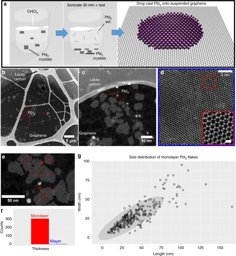
Figure 1a shows the schematic diagram of the liquid exfoliation experimental procedure. The sonication time is important for controlling the exfoliation of PbI2. Less sonication leaves multilayer PbI2 dispersed in the solution, whereas longer sonication time renders very small flakes or completely destroys the sheets (Supplementary Note 1). Moreover, the supernatant used for dropcasting also plays a role, and only the solution from the top has been used (Supplementary Note 2). Our results show successful exfoliation of mostly monolayer flakes of the PbI2 from its bulk counterpart. Moreover, the dispersed solution was found to be stable for a considerable number of days. Even after a week of the sonication process, we could still observe monolayer flakes dispersed in the solution (Supplementary Note 1). Out of >300 flakes studied in this experiment, we only found 2 flakes with bilayer structure (Supplementary Note 3), whereas all others were monolayers. Some nanoparticles that are observed come from the graphene underneath and not from PbI2 itself (Supplementary Note 4). Figure 1b–d shows the ADF-STEM images of the monolayer PbI2 suspended on monolayer graphene on a TEM grid at various magnifications. The length and width of ~300 flakes was measured (Fig. 1e, f), giving ~42 and 28 nm, respectively, with bigger flakes ranging to >160 nm in size (Fig. 1g).
Fig. 1. Schematic diagram for liquid exfoliation and results.
a Schematic of the LPE synthesis of monolayer PbI2 flakes and deposition on to suspended graphene. b, c ADF-STEM image of monolayer PbI2 flakes at different magnifications. d Atomic resolution ADF-STEM image of a monolayer PbI2 flake. The inset in the figure shows an atomic resolution image of the structure. The scale bar is 0.5 nm. e Typical method for measuring the length(l) and width(w) of the monolayer flake. f Histogram showing the thickness distribution of PbI2 flakes. g Plot of the size distribution for >300 monolayer flakes. Overlapping sizes of different flakes show darker color for their marker dots. The oval represents the highest congregation of flake sizes in the overall sample distribution.
1-H structural phase
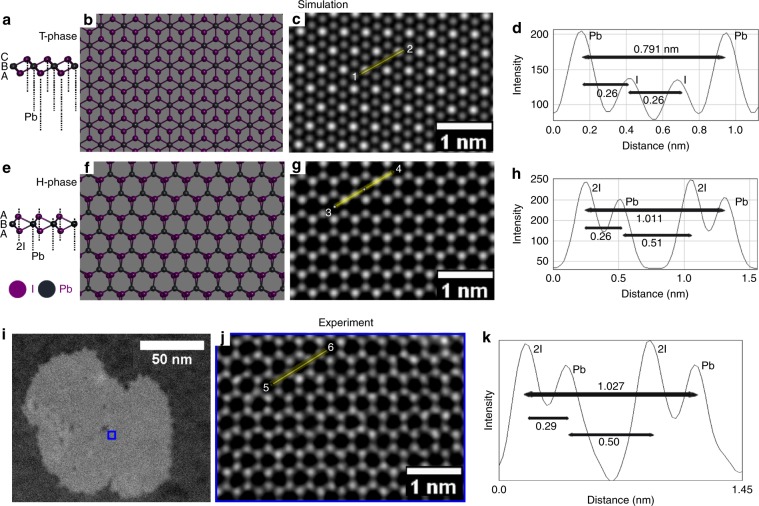
The bulk crystal structure of PbI2 has a CdI2 structural type with lead and iodide layers stacked together in ABC instead of ABA stacking. However, in the monolayer form there are two structural phases, namely—1-H phase and 1-T phase. PbI2 has similar structures to the TMDs (MoS2 and WS2), where the metal (Pb) atomic plane is in the middle and the two iodide atomic layers at the top and the bottom. A monolayer from a 2 H PbI2 bulk crystal structure (Fig. 2a) of PbI2 typically has a 1-T phase (Fig. 2b), where the two iodide atoms do not share the same z-axis and are located in an octahedral coordination. Whereas the 1-H phase of monolayer PbI2 (Fig. 2e, f) has two iodide atomic layers on top of each other in a trigonal-prismatic coordination, as shown in Fig. 2e, f respectively. The position of the Pb and I atoms can be determined by their contrast in ADF-STEM images. Pb has Z = 82, I has Z = 53, and 2I has Z = 106, which means that the 2I positions will have higher contrast than the single Pb. The line profiles (Fig. 2d, h) of the multislice image simulations for 1 T and 1 H PbI2 monolayers give the distance across 1− > 2 and 3− > 4 in Fig. 2c, g, respectively, for comparison to our experimental data (Fig. 2i–k). The experimental Pb–Pb distance of 1.027 nm and the inter-atomic Pb–2I distances are in excellent agreement with the simulated distances of the 1 H structural type (Fig. 2h). To further validate the case of monolayer 1 H structure, we bombarded the nanodisks with electron beam. And as seen in Supplementary Note 5, post few minutes of beam exposure, the agglomeration of vacancies lead to hole formation. Previous studies have reported that the initial defect or hole formation occurs layer-wise instead38,48. Since, the hole formation revealed no further layers underneath, it is conclusive to say that this is a monolayer structure instead of AA′-stacked bilayer 1 H structure.
Fig. 2. Atomic resolution ADF-STEM analysis of monolayer 1 H and 1 T phase.
a Side view of the 1 T atomic structure of PbI2. b Top view of the 1 T atomic model of single layer PbI2. c Multislice ADF-STEM image simulation of the 1 T atomic model in b. d Line profile of the lead and iodide intensities marked with yellow line in the atomic model in c, along the direction 1-2. e Side view of 1 H monolayer atomic crystal structure of PbI2. f Top view of the 1 H atomic model of single layer PbI2. g Multislice ADF-STEM image simulation of the 1 H atomic model shown in f. h Line profile of the lead and iodide intensities marked with yellow line in the atomic model in g, along the direction 3–4. i Low-magnification ADF-STEM image of a monolayer PbI2 flake suspended on graphene. j Higher magnification of the region indicated by the blue box in i, showing the 1 H atomic structure. k Line profile taken from region marked by the yellow box in j, which corresponds to same position with the region marked in simulation g, along the direction 5–6.
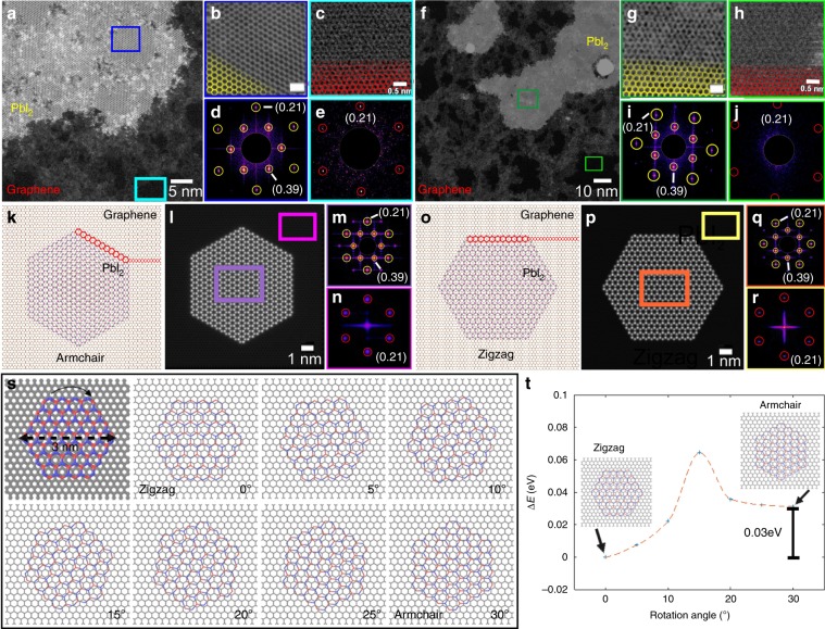
The 1 T phase is expected to be more stable than the H phase with total energy 165 meV per unit cell lower49, unlike the other 2D materials such as MoS2, where the 1 H phase is generally known to be more stable than the 1 T phase50. However, all PbI2 flakes suspended on graphene, from smallest 3 nm to larger hundreds of nanometers in size (Supplementary Note 6), showed 1 H phase, attributed to epitaxial interactions with the underlying graphene support. Chemical vapor deposition (CVD)-grown graphene has grain boundaries with random orientation and hence, we saw that PbI2 flakes within a region (1–5 µm) showed the same relative crystal orientation relative to the graphene crystal (Supplementary Note 7, Supplementary Note 8)50,51. To confirm the case of PbI2–graphene interactions, we deposited PbI2 flakes directly on top of lacey carbon TEM grids without graphene, and observed PbI2 flakes with 1 T structure instead (Supplementary Note 9). We also carried a time-dependent study and concluded that the spatial variations in the PbI2 lattice occurred during the early stages after deposition on graphene, eventually completely transforming to well-defined 1 H phase over time (Supplementary Note 10). After 1 day, all the PbI2 flakes on graphene showed well-defined 1 H phase with the same orientations in a given area. To understand why PbI2 adopts 1 H structure with concomitant alignment to the armchair direction of graphene, we examine the Moire patterns formed between the two crystals (Supplementary Note 11). The best lattice match occurs when the PbI2 adopts 1 H phase and is aligned to the armchair direction, which agrees with our experimental findings.
Interestingly, we also found that the crystal orientation of PbI2 on graphene had preferred orientation of PbI2 zigzag aligned to graphene armchair direction, with only a small fraction showing the zigzag to zigzag alignments. Figure 3a, f shows the ADF-STEM images and their FFTs of the two different types of orientations of PbI2 on graphene. Figure 3k–r shows the atomic models of PbI2 on graphene for the two aligned directions and the multislice image simulation, along with the fast Fourier transform (FFT) results matching the experimental data. To understand why PbI2 adopts 1 H structure with concomitant alignment in these particular directions of graphene, we employed density functional theory (DFT) calculations to study the structural and energetic stability of the different alignments. We used a short-range relaxed atomic model of PbI2 on graphene, as shown in Fig. 3s, and rotated it every 5 degrees (Fig. 3s) to find the most energetically stable heterostructure (Fig. 3t). This also confirms our results to how the graphene influences the stability of the PbI2 and leads to these energetically favorable structure that are also observed in the experimental results.
Fig. 3. Crystal orientation of monolayer PbI2 on graphene.
a ADF-STEM images of PbI2 flake suspended on graphene. b High-resolution image of PbI2 crystal annotated in the dark blue box in a. Scale bar corresponds to 1 nm. c High-resolution image of graphene taken from the cyan box region indicated in a. d FFT of PbI2 from the region indicated in b. c FFT of graphene from the region indicated in c. f ADF-STEM images of PbI2 flake suspended on graphene. g High-resolution image of PbI2 crystal indicated by the dark green box in f. Scale bar corresponds to 1 nm. h High-resolution image of graphene from the light green box in f. i FFT of PbI2 from the region indicated in g. h FFT of graphene from the region indicated in f. k Atomic model of PbI2 (1 H) on graphene in the armchair direction. l Multislice image simulations based on the atomic model in k. m FFT of PbI2 from the region indicated by the purple box in l. n FFT of graphene from the region indicated by the pink box in l. o Atomic model of PbI2 (1 H) on graphene in the armchair direction. p Multislice image simulations based on the atomic model in k. q FFT of PbI2 from the region indicated by the orange box in p. r FFT of graphene from the region indicated by the yellow box in p. s Atomic models showing PbI2 relative to graphene for s DFT-relaxed atomic model of PbI2 on graphene, rotated every 5 degrees. t Energy profile of various orientation angles of the PbI2 flake on graphene.
Structural defects
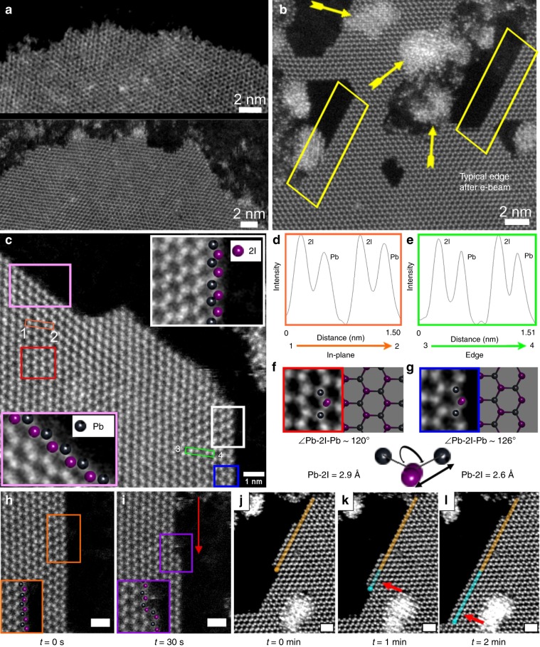
Next, we examine the edge terminations of PbI2, because edges of 2D materials can influence the electrical, chemical, and catalytic properties due to the different bonding (angles, bond distances, etc.) between atoms51–54. Fig. 4a shows the typical edges of two different monolayer PbI2 flakes, just after being deposited on the graphene. The edges are rough and do not appear to be highly faceted to a specific crystal lattice direction. After electron beam irradiation (Fig. 4b), the edges are etched to form sharp zigzag-faceted terminations (Fig. 4c). The zigzag edges have iodide atoms protruding out on one side and lead atoms on the adjacent edge of the same flake (Fig. 4d, e). Metal and chalcogenide-terminated zigzag edges have been routinely observed for as grown monolayer TMDs, such as MoS255,56. However, in this case, the edge etching also happened in directions which maintained the zigzag-PbI2 alignment to the armchair graphene direction (Supplementary Note 12).
Fig. 4. Edge study of PbI2.
ADF-STEM image of a typical intrinsic edges of two different monolayer PbI2 flakes just after deposition on the graphene and b sharp zigzag-faceted edges of the monolayer PbI2 flake after electron beam irradiation. The arrows show the clustering of the atoms after having been sputtered out of the edges. The yellow boxes show the faceted zigzag edge formation from the intrinsic edges after the damage from electron beam. c ADF-STEM images showing I- and Pb-terminated zigzag termination. The two insets in the image shown with white and pink boxes show the high resolution of the areas with same color annotation that have I- and Pb-terminated edges. The line profile of the regions marked in orange and green boxes confirms the position of the lead and iodide in the honeycomb structure. d, e The line profile of the orange and green boxes shown in c, in the direction of 1–2 and 3–4. f High-resolution ADF-STEM image of the area shown under red box in c. g High-resolution ADF-STEM image of the area shown under blue box in c. h, i Time-lapse ADF-STEM image of the edge at t = 0 s and t = 30 s of electron beam exposure. The red arrow indicates the ejection of the electrons from the edges due to the damage from the electron beam, leading to ‘unzipping’ of the chain, maintaining the zigzag edge of the flakes. j–l Time-lapse series of ADF-STEM images recorded after 1 min of electron beam exposure. The yellow annotations show the edge-terminated bonds at the edge at t = 0 s, which starts reconstructing in k, annotated with blue. After 2 min, (l) the edge was fully reconstructed, as shown with growing blue annotated region. The scale bars in h–l correspond to 1 nm.
Edge etching occurred by atomic loss under the electron beam (Fig. 4h–i), and edges also showed atomic attachment to restructure (Fig. 4j–l, Supplementary Note 13). After 30 s of electron beam exposure, the atoms at the edge are sputtered out, by unzipping the outer most atoms to retain its uniform zigzag termination (Fig. 4i)56. Prolonged exposure to the electron beam eventually leads to edge roughening. DFT and ab initio molecular dynamics simulations have shown the edge reconstructions effect the electrical and magnetic properties of the material57.
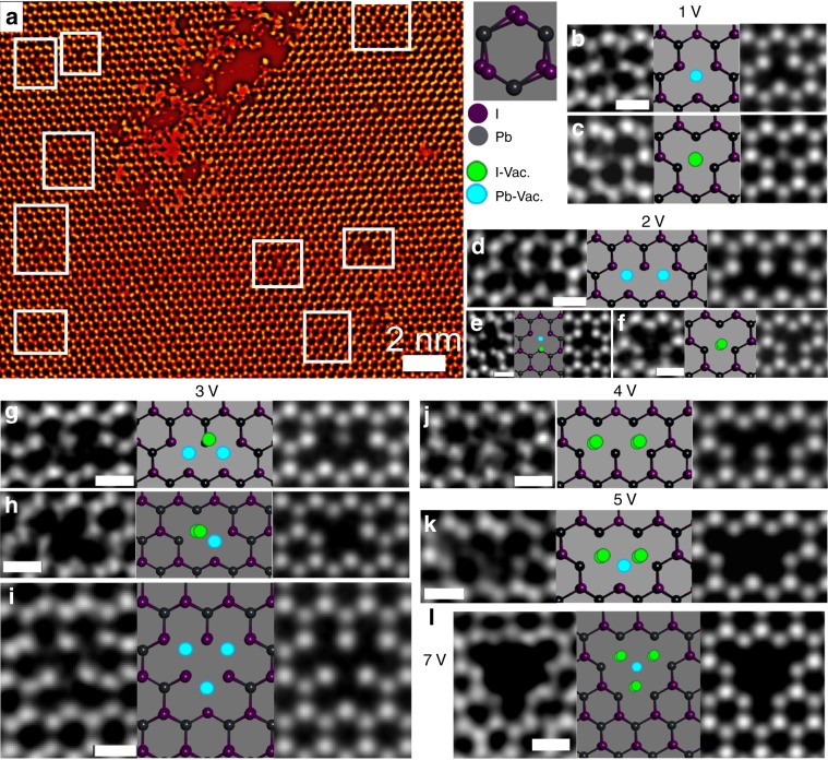
ADF-STEM of the central lattice region of the PbI2 monolayers revealed point defects across the region (Fig. 5a). Single-point vacancies were observed for both the lead and iodide sub-lattice sites in PbI2 (Fig. 5b, c), and identified using line profiles (Supplementary Note 14). The energy to remove a single iodide or lead atom from the lattice into the vacuum was calculated by DFT to be 3.15 and 6.36 eV, respectively (Supplementary Note 15). The maximum amount of energy (E) transferred by an incident electron (@80 keV) to a single iodide or lead atom is calculated to be 1.38 and 0.85 eV, respectively58. This energy transfer from the incident electron to the specimen atoms is much lower than the required sputtering energy calculated by DFT. Hence, we can deduce that the mechanism of damage in this system is more complicated than purely knock-on damage from atomic sputtering, and likely involves radiolysis. This is not surprising, since PbI2 is a large bandgap semiconductor and therefore prone to ionization effects from the electron beam. Several different types of multiple atom point vacancies are identified, ranging from two atoms (Fig, 5d, e) to the seven atom defect clusters (Fig. 5k). Vacancies did not appear to assembly into linear structures, as in TMDs, but instead aggregated to form clusters (Supplementary Note 16).
Fig. 5. Vacancy study in monolayer PbI2.
a Low-magnification ADF-STEM image of monolayer PbI2 region after electron beam exposure. The purple and gray spheres correspond to lead and iodide in the structure. The green and blue spheres correspond to the iodide and lead vacancies in the system. ADF-STEM images and their corresponding 1 H PbI2 structured atomic model, as well as multislice simulations have been shown for b point defect with a missing lead atom, c point defect with a missing iodide atom, d double-point defect with two iodide atoms missing, e double-point defect where two lead atoms from adjacent crystal cells are lost, and f double-point defect with one lead and one iodide atoms missing. It can be observed that the single iodide has lower intensity than that of lead or two iodides, g three vacancies formed out of two lead and one iodide loss. It can be observed that the remaining single iodide in the middle has lower intensity than that of lead or two iodides, h three vacancy formed by the absence of three lead atoms from adjacent crystal cells, i another three vacancy formed by two iodide and one lead loss, j four vacancy defect formed by loss of two iodine from adjacent honeycomb structures, k five vacancies formed because of loss of four iodide atoms and a lead atom in a row, l bigger triangular defect formed because of the loss of one lead and six iodide atoms from the center. The scale bar in all the images indicate 0.5 nm.
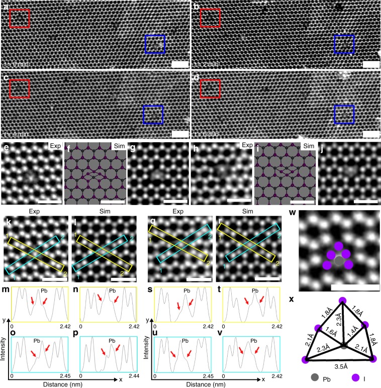
We also observed multiple occasions where the defect (Fig. 6) had one Pb atom in the center and five iodide atoms surrounding it, which was stable even under prolonged electron beam irradiation (Fig. 6a–d). Figure 6f, g,i, j shows the proposed atomic model and the simulation of the two different configurations of this defect, (Fig. 6e, h) respectively. Since a single iodide atom is much lighter (Z = 53) than the single Pb atom (Z = 82), it has lower contrast in ADF-STEM. The line profiles in Fig. 6 confirm the presence of iodide atoms close to the lead atom in the center, causing the iodide peaks to be only partially resolved and forming a tail either side of the lead atom. Figure 6x shows the structure of the system, where Pb is coordinated with five other iodide atoms with inter-atomic distance varying from 1.4–2.3 Å. We observed the formation of a stable four-membered ring around the lead atoms (Fig. 6f, i), where the lighter iodide atoms substitute the heavier lead atoms (Fig. 6f). Similar stable four-membered ring configuration have also been reported for monolayer MoS2 structures59.
Fig. 6. Stable defect dynamics in PbI2.
a–d Time-lapse ADF-STEM images taken after every 2 min. The red and blue boxes show the two different orientations of the substitutional defect, which is rather stable under the electron beam exposure. e ADF-STEM image of a defect with lead in the center and surrounded by five other iodide atoms. f Atomic model that shows the atomic model of the corresponding experimental result. g Multislice image simulations based on the atomic model in f, schematically illustrating the lower intensity of the single iodide atoms surrounding the lead, which agrees with the experimental data in e. m, n Line profile taken across the lead and iodide atoms across the yellow annotated regions in the experimental data k and multislice simulated image in l. The red arrow shows unresolved iodide peaks around the lead. o, p Line profile taken across the lead and iodide atoms across the blue annotated region in k and l, respectively. The red arrow shows unresolved iodide peaks around the lead. j, h ADF-STEM image of the opposite orientated substitutional defect. i Atomic model that shows the atomic model of the corresponding experimental result. j Multislice image simulations based on the atomic model in i, schematically illustrating the lower intensity of the single iodide atoms surrounding the lead, which agrees with the experimental data in h. s, t Line profile taken across the lead and iodide atoms across the yellow annotated regions in the experimental data q and multislice simulated image in r. The red arrow shows unresolved iodide peaks around the lead. u, v Line profile taken across the lead and iodide atoms across the blue annotated region in q and r, respectively. The red arrow shows unresolved iodide peaks around the lead. w Annotated image of e. x Distance between the different atoms shown in the annotated region in w. Scale bars in a–d correspond to 2 nm, whereas in the rest of the images correspond to 1 nm.
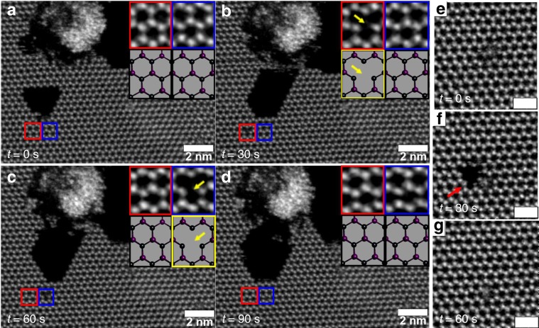
During electron beam irradiation, the vacancies migrated through the lattice and reconstructed. We performed DFT calculations for vacancy migration and found that the energy barrier for migration of lead atom, the in-plane migration of the iodide atom and the out-of-plane migration of iodide atom that corresponded to 0.32, 0.22, and 0.07 eV, respectively (Supplementary Note 17). The energy barrier for migration of the atoms on the surface is considerably lower than the energy imparted from the electron beam and thus explains the quick migration of the vacancies and defects in the system. Figure 7 is an example of a double iodide vacancy (Fig. 7b) and its migration (Fig. 7c) before subsequently healing to render the original structure in Fig. 7a, d. Defect healing occurred in point defects and also with in multiple atom vacancies, such as Fig. 7e–g, where a large defect with seven atoms missing (one Pb and six I) is healed.
Fig. 7. Point defect formation, migration, and then reconstruction.
a–d Time series of ADF-STEM images recorded after every 30 s, of point defect formation, migration, and then reconstruction. The inset under red and blue boxes in the images are high-magnification images of the defects that have been marked with smaller red and blue boxes, respectively, in the same image. The inset figures in black and yellow boxes below the high-magnification insets are the corresponding atomic models. The yellow boxes and arrows in b and c highlights the formation of a point vacancy and its migration in the inset above, before finally reconstructing in d. e–g Time series of ADF-STEM images recorded at an accelerating voltage of 80 kV after every 30 s of electron beam exposure. The red arrow in f shows the formation of seven vacancy defect, but it gets quickly reconstructed in image g after another 30 s of exposure. The scale bars in e–g correspond to 1 nm.
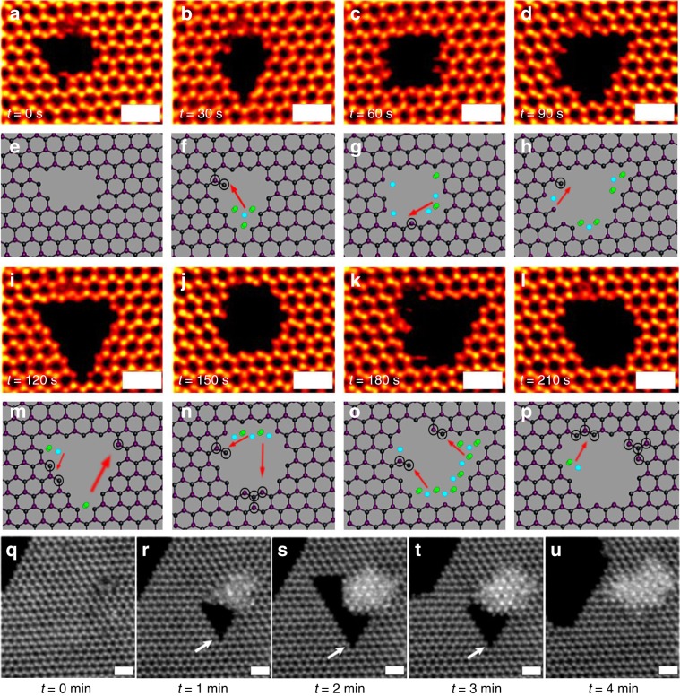
Further electron beam exposure caused the vacancies grow larger and form nanopores in monolayer PbI2 crystals60,61. The nanopores undergo geometric reconstructions by atomic loss (Fig. 8a–p), but also sometimes gain atoms (Fig. 8o–p). Diffusing Pb and I atoms add to the edge sites of the nanopores to enable reconstruction. The nanopores in general adopt zigzag edge terminations and have triangular or hexagonal shape. In several cases, atoms migrate from one side of the nanopore to another side to change the nanopore shape. Figure 8q–u shows a case, where a large triangular nanopore is formed by electron beam irradiation, and is then backfilled by its nearby atoms. Between Fig. 8s, t, the top left section of the triangular nanopore has contracted by atoms filling it in from the nearby edge region. The red arrows indicate the possibility of migration of the atoms from one position to the other. The electron beam damages the material and forms the nanopore but at the same time, we are able to see the fast migration of atoms and the self-healing process in the material in real time. However, prolonged exposure to the electron beam ultimately leads excessive sputtering of atoms than the self-healing itself leading to a bigger nanopore formation. Similarly, in Fig. 8q–u, the self-healing is not perfect, but the nanopore is no longer present and vacancies have been eliminated by the migration to the edge.
Fig. 8. Nanopore geometric reconstructions.
a–p Time series of ADF-STEM images, and their corresponding atomic models. Holes can be seen to change its shape in monolayer PbI2 flake. The blue atoms correspond the lead defect region and the green corresponds to the iodide defect region. The black circles around the atoms in the atomic models correspond to the new atomic bond in the structure as compared from the previous frame. q–u Time series of ADF-STEM images recorded after every 1 min of electron beam exposure. The defect starts forming after 1 min, in image r and more atoms are ejected to form a bigger defect in s. Then the atoms at the edge starts ejecting out in t and reconstruction of the flake starts occurring leading to again defect-free surface in u.The scale bar in all images corresponds to 1 nm.
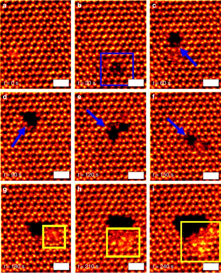
We also observed the migration of entire nanopores as a single entity, up to 4 nm on the same monolayer flake. Figure 9a–i is set of time lapsed images, taken every 30 s, of hole formation and reconstruction as well as migration on the same monolayer flake upon beam exposure. The yellow boxes in Fig. 9g–i show the accumulation of the atoms at the edge and surface region next to the nanopore. The quick variation in the position and size of these holes clearly show how mobile the lead and iodide atoms are on the surface and continuously try to form new structures.
Fig. 9. Nanopore migration.
a–i Time series of ADF-STEM images recorded of nanopores changing form, as well as migrating large distances within single-monolayer PbI2 flake. The scale bar corresponds to 1 nm.
Discussion
We have successfully shown the liquid exfoliation of PbI2 using chloroform and formation of >99% monolayer nanodisks. This approach has the potential to be scaled up to produce a large amount of exfoliated PbI2. Direct imaging of the monolayer PbI2 nanodisks is challenging using conventional TEM grids, and the use of graphene was critical for high-resolution ADF-STEM imaging. However, the van der Waals interactions with the underlying graphene lattice causes epitaxial alignment of the PbI2 and leads to the observation of the 1 H crystal phase for PbI2, with no observation of 1 T phases on graphene. The relative lattice spacing of PbI2 and graphene results in preferential alignment of the PbI2 zigzag direction to the armchair direction of graphene to maximize the commensuration of the two lattices. Integrating monolayer PbI2 with other 2D materials provides a huge scope for many applications and the ability to manipulate its atomic monolayer structure provides a unique opportunity to tune its properties. Studying the influence of the substrate on the structure of PbI2 would hopefully make it easier to understand the complicated polytypes and stacking arrangement in PbI2. ADF-STEM imaging of the PbI2 monolayers revealed highly mobile point vacancies and their growth into nanopores, which exhibited reconstructions and self-healing. Studying these vacancies in the 2D material is important for the foundation knowledge of the semiconducting properties for future work.
Methods
Chemical vapor deposition growth of graphene
Graphene was synthesized by CVD on a copper substrate. A piece of copper foil was first sonicated in a diluted hydrochloric acid solution (1 mol/L) to remove the oxides on the copper surface. The copper foil was then sonicated in deionized water, acetone, and isopropanol for 5 min each to remove organic residues. To ensure uniformity of temperature during the whole growth process, the copper foil was positioned in the center of a furnace. A total of 1% methane in argon (CH4), 25% hydrogen in argon (H2), and 100% argon (Ar) were used for graphene synthesis. Before the reaction started, the system was first purged with 1000 sccm Ar, 500 sccm H2, and 100 sccm CH4 for 30 min. The furnace was then heated to 1060 °C with a ramp rate of 50 °C/min accompanied by a flow of 500 sccm Ar and 100 sccm H2. When the temperature reached 1060 °C, the copper was then annealed with the same flow rate for 1 h. Following the annealing process, the synthesis was carried out at 1060 °C for 1 hr with a flow of 500 sccm Ar, 100 sccm H2, and 5 sccm CH4. The furnace was removed from the sample, which allowed the sample to be fast cooled to room temperature.
Liquid-phase exfoliation
PbI2 powder from Sigma–Aldrich (99% purity) was added to chloroform to form a solution of concentration 1 mg/ml (~0.2 mM). The solution was sonicated in an unheated ultrasonic water bath (Ultrasonics effective output of 200 W; Ultrasonics peak power of 600 W; Ultrasonics operating frequency 30–40kHz) for ~30 min to make sure that all the lead iodide had exfoliated and dispersed in the solution. The dispersion was then left to stand for 24 h to let the bulk particles to settle down at the bottom of the container. Then, the supernatant of the dispersion (from the top) was extracted with a pipette and used for preparing TEM samples.
TEM sample preparation
Graphene was transferred onto a lacey carbon copper 400 mesh TEM grid using a poly (methyl methacrylate (PMMA) support and then the PMMA removed by acetone. It was then subsequently cleaned by Ar/H2 and vacuum annealing. A few drops (10–20 μl each) were taken from the supernatant of the dispersed solution of 1 mg/ml concentration of PbI2 in CHCl3 and dropcasted on to the TEM grid containing suspended graphene. The TEM holder was then baked in high vacuum at 60 °C to remove all the solvents and other impurities from the surface.
Scanning transmission electron microscopy
Room temperature ADF-STEM imaging was performed using a JEOL ARM200F located at the David Cockayne Centre for Electron Microscopy (DCCEM) within the Department of Materials at the University of Oxford. An acceleration voltage of 80 kV was used for taking all the images, unless stated otherwise. Imaging conditions used a 30 µm condenser lens (CL) aperture with a convergence semiangle of 22.5 mrad and a beam current of 35 pA. The acquisition angles for these images was 70–220 mrad.
Data processing
Images were processed using the ImageJ software. Atomic models were constructed using Accelrys Discovery Studio Visualizer. Multislice image simulations were performed using JEMS. PbI2 crystal structure was drawn using Crystal Maker Version 10.3.1.
DFT calculation
The structural, energetic, and defect migration calculations in this work are based on DFT implemented in the Vienna Ab-initio Simulation Package (VASP)62,63. A 10 × 10 × 1 supercell is used for calculating the sputtering energy and defect migration barriers, and two more different systems are designed to probe the short-range angle dependence of stacking energy: a hexagonal PbI2 flake (side length four PbI2 unit cells, 1.8 nm) on continuous graphene substrate. The systems are varied with different angles between PbI2 and graphene (i.e., armchair to zigzag stacking order). The elements are represented by projector-augmented wave potentials with 500 eV energy cutoff and the four (6s26p2) valence electrons for Pb, seven (5s25p5) for I, and four (2s22p2) for C are treated explicitly64,65. Initial relaxation and energetics are calculated via the generalized gradient approximation, Perdew−Burke−Ernzerhof, augmented by DFT-D3 method with Becke–Jonson damping for the interlayer dispersive interaction66,67. The first Brillouin zone is sampled by the tetrahedron method on a 4 × 4 × 1 k-mesh for the 10 × 10 × 1 supercell, and only gamma point for the angle-dependence studies. All structures are relaxed until the force on each atom is <0.01 meV/Å. The sputtering energy is defined by the energy difference between the crystalline structure and the one with a vacancy, for instance, the I sputtering energy is . The energy tolerance is set to 0.0001 for all energy calculations. The minimum energy paths for defect migration are determined by the nudged elastic band (NEB) method68,69. A total of 10 × 10 supercells and 4 × 4 k-point grids are employed, and a criterion of 0.03 eV/Å is set for the force convergence. For VI migration, two pathways are considered: in-plane and out-of-plane directions, and only in-plane VPb migration is considered. The starting and end points for NEB search are prepared by removing the corresponding atoms from the relaxed pristine structure, and then further relaxed. The six intermediate images are interpolated by the Vasp TST toolkit70. The converged energy paths are the fitted by cubic spline functions.
Supporting information
Effect of sonication duration and dropcasting, monolayer and bilayer PbI2 intensity contrast, graphene sample without PbI2, different sizes of monolayer PbI2, proof of monolayer flakes instead of bilayer AA′ 1 H structure, T-phase structure on lacey carbon TEM grid, ADF-STEM images of structural transformation immediately after dropcasting on graphene, Moire pattern of 1 T and 1 H atomic models on graphene, zigzag alignment of PbI2 with graphene after edge etching, relative alignment of time frame of PbI2 etching from Fig. 4, line profile from Fig. 5, DFT calculation of sputtering energy of lead and iodide, accumulation of lead particles after etching, and DFT calculation of vacancy migration.
Supplementary information
Acknowledgements
J.H.W. thanks the support from an ERC Consolidator Grant (LATO 725258). S.S. thanks the joint committee of Linacre College and MPLS division of the University of Oxford for financial support through the Women in Science Scholarship and EPSRC studentship. The authors acknowledge use of characterization facilities within the David Cockayne Centre for Electron Microscopy, Department of Materials, University of Oxford.
Author contributions
S.S. and J.H.W conceived the idea for the project, designed the experiments and analysis procedure. S.S. carried out all the chemical synthesis and experiments. S.S. carried out analysis of data and wrote the manuscript with contributions from J.H.W. Y.S. synthesized monolayer graphene. T.Z. and A.F.L carried out the DFT calculation. J.C.G. and K.P. provided materials for the experiments and helped with scientific discussions. J.H.W. supervised the project. All authors discussed the results and commented on the manuscript.
Data availability
Experimental procedures and characterization data are available within this article and its Supplementary Information file. The data that support the findings of this study are available from the corresponding authors upon reasonable request.
Competing interests
The authors declare no competing interests.
Footnotes
Peer review information Nature Communications thanks the anonymous reviewer(s) for their contribution to the peer review of this work. Peer reviewer reports are available.
Publisher’s note Springer Nature remains neutral with regard to jurisdictional claims in published maps and institutional affiliations.
Supplementary information
Supplementary information is available for this paper at 10.1038/s41467-020-14481-z.
References
- 1.Wang QH, Kalantar-zadeh K, Kis A, Coleman JN, Strano MS. Transition metal dichalcogenides. Nat. Nanotech. 2012;7:699–712. doi: 10.1038/nnano.2012.193. [DOI] [PubMed] [Google Scholar]
- 2.Mak KF, He K, Shan J, Heinz TF. Control of valley polarization in monolayer MoS2 by optical helicity. Nat. Nanotech. 2012;7:494–498. doi: 10.1038/nnano.2012.96. [DOI] [PubMed] [Google Scholar]
- 3.Zeng H, Dai J, Yao W, Xiao D, Cui X. Valley polarization in MoS2 monolayers by optical pumping. Nat. Nanotech. 2012;7:490–493. doi: 10.1038/nnano.2012.95. [DOI] [PubMed] [Google Scholar]
- 4.Elias DC, et al. Dirac cones reshaped by interaction effects in suspended graphene. Nat. Phys. 2011;7:701–704. doi: 10.1038/nphys2049. [DOI] [Google Scholar]
- 5.Radisavljevic B, Radenovic A, Brivio J, Giacometti V, Kis A. Single-layer MoS2 transistors. Nat. Nanotech. 2011;6:147–150. doi: 10.1038/nnano.2010.279. [DOI] [PubMed] [Google Scholar]
- 6.Amani M, et al. Vapor deposition electrical performance of monolayer MoS2 field-effect transistors prepared by chemical vapor deposition. Appl. Phys. Lett. 2013;102:193107. doi: 10.1063/1.4804546. [DOI] [Google Scholar]
- 7.Ganatra R, Zhang Q. Few-layer MoS2: a promising layered semiconductor. ACS Nano. 2014;5:4074–4099. doi: 10.1021/nn405938z. [DOI] [PubMed] [Google Scholar]
- 8.Lv R, et al. Transition metal dichalcogenides and beyond: synthesis, properties, and applications of single- and few-layer nanosheets. Acc. Chem. Res. 2015;48:56–64. doi: 10.1021/ar5002846. [DOI] [PubMed] [Google Scholar]
- 9.Schwierz F, Pezoldt J, Granzner R. Two-dimensional materials and their prospects in transistor electronics. Nanoscale. 2015;7:8261–8283. doi: 10.1039/C5NR01052G. [DOI] [PubMed] [Google Scholar]
- 10.Zhou M, Duan W, Chen Y, Du A. Single layer lead iodide: computational exploration of structural, electronic and optical properties, strain induced band modulation and the role of spin-orbital-coupling. Nanoscale. 2015;7:15168–15174. doi: 10.1039/C5NR04431F. [DOI] [PubMed] [Google Scholar]
- 11.Zhong M, et al. Large-scale 2D PbI2 monolayers: experimental realization and their indirect band-gap related properties. Nanoscale. 2017;9:3736–3741. doi: 10.1039/C6NR07924E. [DOI] [PubMed] [Google Scholar]
- 12.Toulouse AS, et al. Frenkel-like Wannier-Mott Excitons in few-layer PbI2. Phys. Rev. B. 2015;19:165308. doi: 10.1103/PhysRevB.91.165308. [DOI] [Google Scholar]
- 13.Arbiol J, et al. Whispering gallery mode lasing from hexagonal shaped layered lead iodide. ACS Nano. 2015;9:687–695. doi: 10.1021/nn5061207. [DOI] [PubMed] [Google Scholar]
- 14.Zhengqi S, Jayatissa AH. Perovskites-based solar cells: a review of recent progress, materials and processing methods. Materials (Basel) 2018;11:729. doi: 10.3390/ma11050729. [DOI] [PMC free article] [PubMed] [Google Scholar]
- 15.Niu G, Guo X, Wang L. Review of recent progress in chemical stability of perovskite solar cells. J. Mater. Chem. A. 2015;3:8970–8980. doi: 10.1039/C4TA04994B. [DOI] [Google Scholar]
- 16.Heo J. Development of a stable and sensitive semiconductor detector by using a mixture of lead(II) iodide and lead monoxide for NDT radiation dose detection. JINST. 2018;13:C03023. doi: 10.1088/1748-0221/13/03/C03023. [DOI] [Google Scholar]
- 17.Zhu XH, Wei ZR, Jin YR, Xiang AP. Growth and characterization of a PbI2 Single crystal used for gamma ray detectors. Cryst. Res. Technol. 2007;42:456–459. doi: 10.1002/crat.200610847. [DOI] [Google Scholar]
- 18.Kasap Safa, Frey Joel B., Belev George, Tousignant Olivier, Mani Habib, Greenspan Jonathan, Laperriere Luc, Bubon Oleksandr, Reznik Alla, DeCrescenzo Giovanni, Karim Karim S., Rowlands John A. Amorphous and Polycrystalline Photoconductors for Direct Conversion Flat Panel X-Ray Image Sensors. Sensors. 2011;11(5):5112–5157. doi: 10.3390/s110505112. [DOI] [PMC free article] [PubMed] [Google Scholar]
- 19.Beckmann PA. A review of polytypism in lead iodide. Cryst. Res. Technol. 2010;45:455–460. doi: 10.1002/crat.201000066. [DOI] [Google Scholar]
- 20.Han M, et al. Two-step vapor deposition of self-catalyzed large-size PbI2 nanobelts for high-performance photodetectors. J. Mater. Chem. C. 2018;21:5746–5753. doi: 10.1039/C8TC01180J. [DOI] [Google Scholar]
- 21.Lan C, et al. Large-scale synthesis of freestanding layer-structured PbI2 and MAPbI3 nanosheets for high-performance photodetection. Adv. Mat. 2017;29:1702759. doi: 10.1002/adma.201702759. [DOI] [PubMed] [Google Scholar]
- 22.Tan M, et al. 2D lead dihalides for high-performance ultraviolet photodetectors and their detection mechanism investigation. Small. 2017;13:1–8. doi: 10.1002/smll.201702024. [DOI] [PubMed] [Google Scholar]
- 23.Zheng W, et al. High-crystalline 2D layered PbI2 with ultrasmooth surface: liquid-phase synthesis and application of high-speed photon detection. Adv. Electron. Mater. 2016;2:1–8. [Google Scholar]
- 24.Rybak O, et al. Luminescent spectra of PbI single crystals doped by 3d-metal impurities. J. Lumin. 1998;79:257–267. doi: 10.1016/S0022-2313(98)00041-6. [DOI] [Google Scholar]
- 25.Chang Y, James RB. Phonon dispersion and polar-optical scattering in 2H PbI2. Phys. Rev. B. 1997;55:8219–8225. doi: 10.1103/PhysRevB.55.8219. [DOI] [Google Scholar]
- 26.Cabana L, et al. Synthesis of PbI2 single-layered inorganic nanotubes encapsulated within carbon nanotubes. Adv. Mater. 2014;26:2016–2021. doi: 10.1002/adma.201305169. [DOI] [PubMed] [Google Scholar]
- 27.Fan Q, et al. Liquid exfoliation of two-dimensional PbI2 nanosheets for ultrafast photonics. ACS Photonics. 2019;6:1051–1057. doi: 10.1021/acsphotonics.9b00122. [DOI] [Google Scholar]
- 28.Nicolosi, V.; Chhowalla, M.; Kanatzidis, M. G.; Strano, M. S. & Coleman, J. N. Liquid exfoliation of layered materials. Science, 340, 1226419 (2013).
- 29.Tao H, et al. Scalable exfoliation and dispersion of two-dimensional materials-an update. Phys. Chem. Chem. Phys. 2017;19:921–960. doi: 10.1039/C6CP06813H. [DOI] [PubMed] [Google Scholar]
- 30.Huo C, Yan Z, Song X, Zeng H. 2D materials via liquid exfoliation: a review on fabrication and applications. Sci. Bull. 2015;60:1994–2008. doi: 10.1007/s11434-015-0936-3. [DOI] [Google Scholar]
- 31.May P, Khan U, Hughes JM, Coleman JN. Role of Solubility parameters in understanding the steric stabilization of exfoliated two-dimensional nanosheets by adsorbed polymers. J. Phys. Chem. C. 2012;116:11393–11400. doi: 10.1021/jp302365w. [DOI] [Google Scholar]
- 32.Shen J, et al. Liquid phase exfoliation of two-dimensional materials by directly probing and matching surface tension components. Nano Lett. 2015;15:5449–5454. doi: 10.1021/acs.nanolett.5b01842. [DOI] [PubMed] [Google Scholar]
- 33.Hernandez Y, Lotya M, Rickard D, Bergin SD, Coleman JN. Measurement of multicomponent solubility parameters for graphene facilitates solvent discovery. Langmuir. 2010;3:3208–3213. doi: 10.1021/la903188a. [DOI] [PubMed] [Google Scholar]
- 34.Manna K, Huang HN, Li WT, Ho YH, Chiang WH. Toward understanding the efficient exfoliation of layered materials by water-assisted cosolvent liquid-phase exfoliation. Chem. Mater. 2016;28:7586–7593. doi: 10.1021/acs.chemmater.6b01203. [DOI] [Google Scholar]
- 35.Wang M, et al. Surface tension components ratio: an efficient parameter for direct liquid phase exfoliation. ACS Appl. Mater. Interfaces. 2017;9:9168–9175. doi: 10.1021/acsami.6b16578. [DOI] [PubMed] [Google Scholar]
- 36.Li H, et al. Atomic structure and dynamics of single platinum atom interactions with monolayer MoS2. ACS Nano. 2017;11:3392–3403. doi: 10.1021/acsnano.7b00796. [DOI] [PubMed] [Google Scholar]
- 37.Wang S, et al. Epitaxial templating of two-dimensional metal chloride nanocrystals on monolayer molybdenum disulfide. ACS Nano. 2017;11:6404–6415. doi: 10.1021/acsnano.7b02838. [DOI] [PubMed] [Google Scholar]
- 38.Zhou S, et al. Atomic structure and dynamics of defects in 2D MoS2 bilayers. ACS Omega. 2017;2:3315–3324. doi: 10.1021/acsomega.7b00734. [DOI] [PMC free article] [PubMed] [Google Scholar]
- 39.Brogan MA, Blake AJ, Wilson C, Gregory DH. Magnesium diiodide, MgI2. Acta Cryst. 2003;C59:i136–i138. doi: 10.1107/s0108270103025769. [DOI] [PubMed] [Google Scholar]
- 40.Patnaik, P. Handbook of Inorganic Chemicals. (McGraw-Hill, 2003).
- 41.Clever HL, Johnston FJ. The solubility of some sparingly soluble lead salts: an evaluation of the solubility in water and aqueous electrolyte solution. J. Phys. Chem. Ref. Data. 1980;9:751. doi: 10.1063/1.555628. [DOI] [Google Scholar]
- 42.Hamill JC, Loo Y. Influence of solvent coordination on hybrid organic − inorganic perovskite formation. ACS Energy Lett. 2018;3:92–97. doi: 10.1021/acsenergylett.7b01057. [DOI] [Google Scholar]
- 43.Zhou K, Mao N, Wang H, Peng Y, Zhang H. A mixed-solvent strategy for efficient exfoliation of inorganic graphene analogues. Angew. Chem. Int. Ed. 2011;50:10839–10842. doi: 10.1002/anie.201105364. [DOI] [PubMed] [Google Scholar]
- 44.Cunningham G, et al. Solvent exfoliation of transition metal dichalcogenides: dispersibility of exfoliated nanosheets varies only weakly between compounds. ACS Nano. 2012;6:3468–3480. doi: 10.1021/nn300503e. [DOI] [PubMed] [Google Scholar]
- 45.Cataldo F. A revision of the gutmann donor numbers of a series of phosphoramides including tepa. Eur. Chem. Bull. 2015;4:92–97. [Google Scholar]
- 46.Huggins CM, Pimentel GC, Shoolery JN. Proton magnetic resonance studies of chloroform in solution: evidence for hydrogen bonding. J. Chem. Phys. 1955;23:1244–1247. doi: 10.1063/1.1742249. [DOI] [Google Scholar]
- 47.McCleallan AL, Nicksic SW, Guffy JC. NMR study of hydrogen bonding between chloroform and dimethyl. J. Mol. Spectr. 1963;348:340–348. doi: 10.1016/0022-2852(63)90035-3. [DOI] [Google Scholar]
- 48.Wang S, Robertson A, Warner JH, Robertson A. Atomic structure of defects and dopants in 2D layered transition metal dichalcogenides. Chem. Soc. Rev. 2018;47:6764–6794. doi: 10.1039/C8CS00236C. [DOI] [PubMed] [Google Scholar]
- 49.Bacaksiz C, Sahin H. Single layer PbI2: hydrogenation-driven reconstructions. RSC Adv. 2016;6:89708–89714. doi: 10.1039/C6RA15020A. [DOI] [Google Scholar]
- 50.Zhao W, et al. Metastable MoS2: crystal structure, electronic band structure, synthetic approach and intriguing physical properties. Chem. Eur. J . 2018;24:15942–15954. doi: 10.1002/chem.201801018. [DOI] [PubMed] [Google Scholar]
- 51.Ezawa M. Peculiar width dependence of the electronic properties of carbon nanoribbons. Phys. Rev. B. 2006;2005:1–8. [Google Scholar]
- 52.Kawai T. Graphitic ribbons without hydrogen-termination: electronic structures and stabilities. Phys. Rev. B. 2000;62:349–352.. doi: 10.1103/PhysRevB.62.R16349. [DOI] [Google Scholar]
- 53.Li Y, Zhou Z, Zhang S, Chen Z. MoS2 nanoribbon: high stability and unusual electronic and magnetic properties. J. Am. Chem. Soc. 2008;130:16739–16744. doi: 10.1021/ja805545x. [DOI] [PubMed] [Google Scholar]
- 54.Butler SZ, et al. Progress, challenges, and opportunities in two-dimensional materials beyond graphene. ACS Nano. 2013;7:2898–2926. doi: 10.1021/nn400280c. [DOI] [PubMed] [Google Scholar]
- 55.Wang S, et al. Atomically sharp crack tips in monolayer MoS2 and their enhanced toughness by vacancy defects. ACS Nano. 2016;10:9831–9839. doi: 10.1021/acsnano.6b05435. [DOI] [PubMed] [Google Scholar]
- 56.Wang S, Sawada H, Allen CS, Kirkland AI, Warner JH. Orientation dependent interlayer stacking structure in bilayer MoS2 domains. Nanoscale. 2017;9:13060–13068. doi: 10.1039/C7NR03198J. [DOI] [PubMed] [Google Scholar]
- 57.Sang X, et al. Unocic, in situ edge engineering in two-dimensional transition metal dichalcogenides. Nat. Commun. 2018;9:2051. doi: 10.1038/s41467-018-04435-x. [DOI] [PMC free article] [PubMed] [Google Scholar]
- 58.Egerton RF, Li P, Malac M. Radiation damage in the TEM and SEM. Micron. 2004;35:399–409. doi: 10.1016/j.micron.2004.02.003. [DOI] [PubMed] [Google Scholar]
- 59.Zhou S, et al. Atomically sharp interlayer stacking shifts at anti-phase grain boundaries in overlapping MoS2 secondary layers. Nanoscale. 2018;10:16692–16702. doi: 10.1039/C8NR04486D. [DOI] [PubMed] [Google Scholar]
- 60.Chen Q, et al. Ultralong 1D vacancy channels for rapid atomic migration during 2D void formation in monolayer MoS2. ACS Nano. 2018;12:7721–7730. doi: 10.1021/acsnano.8b01610. [DOI] [PubMed] [Google Scholar]
- 61.Russo CJ, Golovchenko JA. Atom-by-atom nucleation and growth of graphene nanopores. PNAS. 2012;109:5953–5957. doi: 10.1073/pnas.1119827109. [DOI] [PMC free article] [PubMed] [Google Scholar]
- 62.Kresse G, Furthmüller J. Efficient iterative schemes for ab initio total-energy calculations using a plane-wave basis set. Phys. Rev. B. 1996;54:11169–11186. doi: 10.1103/PhysRevB.54.11169. [DOI] [PubMed] [Google Scholar]
- 63.Kresse G, Furthmüller J. Efficiency of ab-initio total energy calculations for metals and semiconductors using a plane-wave basis set. Comput. Mater. Sci. 1996;6:15–50. doi: 10.1016/0927-0256(96)00008-0. [DOI] [PubMed] [Google Scholar]
- 64.Blöchl PE. Projector augmented-wave method. Phys. Rev. B. 1994;50:17953–17979. doi: 10.1103/PhysRevB.50.17953. [DOI] [PubMed] [Google Scholar]
- 65.Kresse G, Joubert J. From ultrasoft pseudopotentials to the projector augmented wave method. Phys. Rev. B. 1999;59:1758. doi: 10.1103/PhysRevB.59.1758. [DOI] [Google Scholar]
- 66.Perdew JP, Burke K, Ernzerhof M. Generalized gradient approximation made simple. Phys. Rev. Lett. 1996;77:3865. doi: 10.1103/PhysRevLett.77.3865. [DOI] [PubMed] [Google Scholar]
- 67.Grimme S, Ehrlich S, Goerigk L. Effect of the damping function in dispersion corrected density functional theory. J. Comp. Chem. 2011;32:1456. doi: 10.1002/jcc.21759. [DOI] [PubMed] [Google Scholar]
- 68.Sheppard D, Henkelman G. Paths to which the nudged elastic band converges. J. Comp. Chem. 2011;32:1769–1771. doi: 10.1002/jcc.21748. [DOI] [PubMed] [Google Scholar]
- 69.Sheppard D, Terrell R, Henkelman G. Optimization methods for finding minimum energy paths. J. Chem. Phys. 2008;128:134106. doi: 10.1063/1.2841941. [DOI] [PubMed] [Google Scholar]
- 70.Henkelman G, Jónsson H. Improved tangent estimate in the nudged elastic band method for finding minimum energy paths and saddle points. J. Chem. Phys. 2000;113:9978–9985. doi: 10.1063/1.1323224. [DOI] [Google Scholar]
Associated Data
This section collects any data citations, data availability statements, or supplementary materials included in this article.
Supplementary Materials
Data Availability Statement
Experimental procedures and characterization data are available within this article and its Supplementary Information file. The data that support the findings of this study are available from the corresponding authors upon reasonable request.


