

Abstract
In this paper, it is shown that the sequence of chemical etching of the template and annealing has a significant effect on the shape and spectrum of the nano-metal arrays fabricated by nanosphere lithography (NSL). Higher nanoparticles with sharp edges are fabricated as a consequence of annealing the metal coated template, which is a 2d colloidal crystal, before chemical etching. Consequently, the absorption spectra of the fabricated sample become much sharper, in comparison with the one that is fabricated with the reversed order and also a shift is observed in the peak wavelength. The achieved result has practical importance for the applications of these nano-metal arrays in localized surface plasmon resonance (LSPR) based sensors.
Keywords: Materials science, Nanotechnology, Photonics, Nanomaterials, Nanoparticles, Microstructure, Thin film, Nanosphere lithography, Chemical etching, Annealing, Localized surface plasmon resonance
Materials science; Nanotechnology; Photonics; Nanomaterials; Nanoparticles; Microstructure; Thin film; Nanosphere lithography; Chemical etching; Annealing; Localized surface plasmon resonance
1. Introduction
Among different chemical and physical methods to fabricate 2d nanoparticles arrays [1], [2], [3], [4], [5], [6], nanosphere lithography (NSL) is a cost-effective and simple technique that is first introduced by Van Duyne and his colleagues in 1995 [7]. Understanding the enhancement mechanism of surface-enhanced Raman scattering (SERS) was the initial motivation for fabricating surfaces with periodic nanostructures [8]. On the other side, the collective oscillations of the electron gas in metal nanostructures surrounded by a dielectric is another valuable optical phenomenon with promising applications that is called localized surface plasmon resonance (LSPR) [9]. LSPR based biosensors and chemical sensors are widely used due to their high efficiency and sensitivity [10], [11], [12], [13], [14], [15]. Nobel metals such as silver and gold are the typical materials for fabricating nano-metal arrays for plasmonic applications. Even though silver's LSPR bands are sharper and more intense than the gold's bands, the higher chemical stability of gold nanostructures has been preferred for its sensing applications [16]. The size, shape and composition of the nanoparticles determine the spectral position of LSPR [17], [18], [19], [20]. Also, any variation in the refractive index of the dielectric medium around nanoparticles causes a shift in the spectrum which is the essential property that is used in LSPR based sensors [21]. The first step of the NSL is preparing a template that is a monolayer of polymeric spherical microparticles. Various fabrication methods of the polymeric monolayers such as spin coating [22], electrophoretic deposition [23], [24], dip coating [25] are reported in previous works [26]. Also, self-assembly of monolayers at the liquid-liquid interface [27] and gas-liquid interface [28] are studied widely as they can provide a really easy and fast method for fabrication of monolayers on the substrates. Also, in some techniques, capillary forces in different cells made of some glass slides, play a major role to grow monolayers [29]. An example of this method is two glass slides that are connected to each other from one side and make a small angle that is called wedge-shaped cell [30]. In this paper the template monolayer is prepared by wedge-shaped cells.
The second step is to deposit a metal on the prepared template. The deposition conditions such as the time, the rate and angle of the deposition are other factors that can influence the shape and size of the grown nanoparticles.
The last step is removing the template that is usually done by chemical etching (sonication in an adequate solvent) or by stripping.
To crystallize the sample, an annealing step that can induce a crystallographic phase change is sometimes recommended [31]. In this paper, it is understood that the sequence of the chemical etching and annealing has a noticeable effect on the LSPR extinction spectrum due to its impact on the nanoparticle's size and shape.
2. Experimental
The first step for NSL is preparing a template that is a 2d colloidal crystal of monodisperse spherical polymers. Fabricating a big and uniform template is crucial as a first step. As it was mentioned in the previous section, in this work, the wedge shaped cell method is used to fabricate the template. Different factors need to be optimized to have a centimeter-sized uniform 2d colloidal crystals that were investigated in our previous work [32]. To assemble such a template, first of all, we need to prepare the substrates. After washing the glass substrate with a detergent and rinsing them with distilled water, a nitrogen flux is used to dry them in a stainless manner. Then, by submersing the substrates in piranha solution (, (, Merck, Germany) and (35%, Merck, Germany)) at 100 °C for 1 hour, the substrates become hydrophilized. Next, the substrates are rinsed and dried with distilled water and Nitrogen gas once more. Lastly, a wedge shaped cell with the contact angle of 2.5° is made for growing a monolayer of spherical Polystyrene (PS) beads with the diameter and standard deviation of 508 nm and 0.013 μm, respectively (microParticles GmbH, Germany). Also, relative humidity of 80% and temperature of 10 °C are provided by constant climate chamber (Binder KBF 115, Germany) to have a controlled evaporation rate. Due to the results reported in our previous work [32], the optimized range of concentration for assembly of centimeter-sized uniform 2d colloidal crystals of PS spheres with the diameter of 508 nm is from 1.7 wt.% to 1.85 wt.% that is applied in this work, as well. The next step for the NSL is to deposit the metal on the prepared 2d template. Different metals such as gold, silver and copper are widely used in previous works [33], [34], [35]. Also, in some studies two or more types of metals or metal alloys are applied [36], [37]. In this work, first, sputtering deposition method is used to deposit 5 nm of Ti on the template by means of Magnetron Sputtering (78540 Vernouillet-France). Then, thermal evaporation method, using a Vacuum Coating Unit (HINDHIVAC PVT.LTD (Model:15F6), India), is applied to deposit 50 nm of the gold as a second layer on the template. In order to complete the NSL, there are two important steps: removing the polymeric template, which is done by chemical etching in this work, and annealing. The chemical etching is done be sonicating the substrate in Chloroform (Merck, Germany) and for annealing the substrates are put in an oven (Exciton CO. LTD, Iran) with the temperature of 500 °C for an hour. Due to the obtained results, the sequence of these two steps influences the LSPR extinction spectrum that is measured by UV-VIS Spectrophotometer (Shimadzu UV-2450, Japan). To investigate the reason for such an important difference in the observed spectra of the two samples prepared with different sequences, the shape and size of the nanoparticles in each sample are studied by comparing their scanning electron microscope (SEM) and atomic force microscope (AFM) images (taken by Tuscan MIRA3 FEG-SEM scanning electron microscope, Czech Republic and Nanosurf Mobile S atomic force microscope, Switzerland).
Fig. 1 shows the schematic illustration of the two applied approaches in this work. As it is depicted in this figure, the sequence of two steps, chemical etching and annealing, plays a key role in the final shape and size of the nanoparticles.
Figure 1.

The schematic illustration of two applied methods in this work for fabricating nano-metal arrays.
3. Results and discussion
As a result of applying all optimized conditions, a uniform and big 2d colloidal crystals of PS spheres are fabricated on a glass substrate that its SEM image is shown in Fig. 2(a). Uniform and centimeter-sized templates can cause well-arranged and homogeneous nano-metal array that its SEM image is shown in Fig. 2(b), too.
Figure 2.

(a) the SEM image of a uniform 2d colloidal crystals on a glass substrate, (b) the SEM image of well-arranged nano metal array.
To compare the result of applying the two different methods showed in Fig. 1, first of all, the SEM images of two samples prepared by these methods are displayed in Fig. 3. Fig. 3(a) shows the SEM image of a sample that is annealed after removing the template (Method 1) and Fig. 3(b) shows the SEM image of a sample with reversed sequence (Method 2). These figures show that the final prepared nano-metals have different shapes and sizes. Nanoparticles shown in fig. Fig. 3(b) have sharper edges and they are more triangular like. To investigate the shapes of nanoparticles more, a big area of SEM images of two samples and the threshold of the base area of nanoparticles is shown in Fig. 4. Also, a histogram of the base area of the nanoparticles is plotted in Fig. 5. The histogram shows that the base area of the sample prepared by Method 1 is more uniform in comparison with the other sample. The obtained results show that in Method 1, the chemical etching of the polymers provides more space for nanoparticles to spread during the annealing step that can cause more uniform the base area distribution.
Figure 3.

(a) The SEM image of a sample that is annealed after removing the template (Method 1), (b) The SEM image of a sample that is annealed before removing the template (Method 2).
Figure 4.

(a) The SEM image of a sample prepared by Method 1, (b) the threshold of the base area of nanoparticles in part (a), (c) The SEM image of a sample that is prepared by Method 2 and (d) the threshold of the base area of nanoparticles in part (b). (Parts (b) and (d) are plotted using ImageJ software [38].)
Figure 5.

Histogram of the base area of nanoparticles prepared by (a) Method 1 and (b) Method 2.
Furthermore, to have more insight to the nanoparticles shapes prepared by two proposed methods, the false color map and contour plot of AFM images are displayed in Fig. 6. Having compared these two images, it can be noticed that the nanoparticles's height in sample 1 (Fig. 6(a)) have gradient changes from the peak to the substrate surface. However, somehow flat upper faces can be seen for sample 2 (Fig. 6(b)) that is expected due to the lack of enough space for the gold molecules to slide down during the annealing.
Figure 6.

False color map and contour plot for the samples prepared by (a) Method 1 and (b) Method 2 that is plotted by WSxM software [39].
Also, in order to compare the height and width of the nanoparticles prepared by two proposed methods, the AFM images of the two samples are shown in Fig. 7(a) and (c). The two of the nanoparticles of each sample are chosen and the profile of them is depicted in Fig. 7(b) and (d). As it is clear in this figure, the height of the nano-metals, fabricated by Method 2 (67 nm) are more than the ones fabricated by reversed approach (56 nm). To compare their widths and have a better sight, the profile of the nano-metals created by both methods are displayed in a same figure (Fig. 8). The height distribution function is depicted for the two AFM images shown in Fig. 6 and the result is displayed in Fig. 9. As it was expected, it can be seen that the peak of the function has lower amount for samples prepared by Method 1.
Figure 7.

(a) The AFM image of a sample that is annealed after removing the template (Method 1), (b) the profile of the two nano-metals showed in part (a), (c) the AFM image of a sample that is annealed before removing the template (Method 2) and (d) the profile of the two nano-metals showed in part (c).
Figure 8.

Overlapped profiles of the nano-metals showed on Fig. 7. Dashed line represents the profile of the nano-metals prepared by Method 1 and the solid line show the profile of the nano-metals prepared by Method 2.
Figure 9.
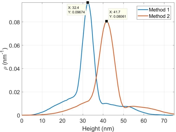
The height distribution function for two AFM images of Fig. 6 obtained by Gwyddion software [40].
All in all, it can be clearly concluded that the shape of the nano-metals can change due to the sequence of chemical etching and annealing. As it is discussed in the literature, the shape of the nanoparticles can highly affect their absorption spectra [41], [42], [43]. So, considering this fact, it is expected to see different absorption spectra for the samples that are fabricated by two above mentioned methods. The absorption spectra of 5 different points on both samples are displayed in Fig. 10(a). The dashed and solid lines represent the spectra of 5 different points on the samples prepared by Method 1 and Method 2, respectively. Also, Fig. 10(b) displayed the average absorption spectra for both methods. As it is seen, the absorption spectrum of the nano-metal arrays fabricated by Method 2, which have higher nanoparticles with sharper edges and also flatter upper sides, is much higher and sharper. Also, the peak wavelength is shifted to a longer wavelength. Due to the fact that recognizing a small shift is much easier in sharper absorption peaks, they are highly-desired in the sensors. Consequently, the samples prepared by Method 2 can be more appropriate for sensing applications of the nano-metal arrays in LSPR based sensors.
Figure 10.

(a) Absorption spectra of the fabricated nano-metals by Method 1 (dashed lines) and Method 2 (solid lines) in 5 different parts of the sample, (b) Average absorption spectra of the fabricated nano-metals by Method 1 (dashed lines) and Method 2 (solid lines).
4. Conclusion
In this work, the effect of the sequence of the chemical etching and annealing on the size, shape and consequently absorption spectra of nano-metal arrays fabricated by NSL was investigated. It was shown that if the annealing was done before chemical etching (Method 2), the higher and thinner nano-metals with sharper edges and also flatter upper sides were fabricated. Thus, the absorption spectra of the prepared sample were much sharper and higher in comparison with the reversed sequence. Also, a red shift was observed in the absorption peak. It was the clear effect of the differences in the shape and size of the nanoparticles prepared by two approaches in this work. So, the concluded fact can have a significant impact on the sensitivity of the LSPR based sensors that are widely used in the present studies due to their high sensitivity.
Declarations
Author contribution statement
Farzaneh Bayat: Conceived and designed the experiments; Performed the experiments; Analyzed and interpreted the data; Wrote the paper.
Habib Tajalli: Conceived and designed the experiments; Contributed reagents, materials, analysis tools or data; Wrote the paper.
Funding statement
This research did not receive any specific grant from funding agencies in the public, commercial, or not-for-profit sectors.
Competing interest statement
The authors declare no conflict of interest.
Additional information
No additional information is available for this paper.
Acknowledgements
The authors thank National Elites Foundation.
References
- 1.Ito T., Okazaki S. Pushing the limits of lithography. Nature. 2000;406(6799):1027. doi: 10.1038/35023233. [DOI] [PubMed] [Google Scholar]
- 2.Courty A., Henry A.I., Goubet N., Pileni M.P. Large triangular single crystals formed by mild annealing of self-organized silver nanocrystals. Nat. Mater. 2007;6(11):900. doi: 10.1038/nmat2004. [DOI] [PubMed] [Google Scholar]
- 3.Henzie J., Lee J., Lee M.H., Hasan W., Odom T.W. Nanofabrication of plasmonic structures. Annu. Rev. Phys. Chem. 2009:60. doi: 10.1146/annurev.physchem.040808.090352. [DOI] [PubMed] [Google Scholar]
- 4.Millstone J.E., Hurst S.J., Métraux G.S., Cutler J.I., Mirkin C.A. Colloidal gold and silver triangular nanoprisms. Small. 2009;5(6):646–664. doi: 10.1002/smll.200801480. [DOI] [PubMed] [Google Scholar]
- 5.Lee J., Hasan W., Stender C.L., Odom T.W. Pyramids: a platform for designing multifunctional plasmonic particles. Acc. Chem. Res. 2008;41(12):1762–1771. doi: 10.1021/ar800126p. [DOI] [PubMed] [Google Scholar]
- 6.Zhang L. Optical conduction resonance in self-assembled metal nanoparticle array-dielectric thin films. J. Nanomater. 2018:2018. [Google Scholar]
- 7.Hulteen J.C., Van Duyne R.P. Nanosphere lithography: a materials general fabrication process for periodic particle array surfaces. J. Vac. Sci. Technol., A, Vac. Surf. Films. 1995;13(3):1553–1558. [Google Scholar]
- 8.Otto A., Mrozek I., Grabhorn H., Akemann W. Surface-enhanced Raman scattering. J. Phys. Condens. Matter. 1992;4(5):1143–1212. [Google Scholar]
- 9.Bohren C.F., Huffman D.R. John Wiley & Sons; 2008. Absorption and Scattering of Light by Small Particles. [Google Scholar]
- 10.Willets K.A., Van Duyne R.P. Localized surface plasmon resonance spectroscopy and sensing. Annu. Rev. Phys. Chem. 2007;58:267–297. doi: 10.1146/annurev.physchem.58.032806.104607. [DOI] [PubMed] [Google Scholar]
- 11.Jain P.K., El-Sayed I.H., El-Sayed M.A. Au nanoparticles target cancer. Nano Today. 2007;2(1):18–29. [Google Scholar]
- 12.Haes A.J., Chang L., Klein W.L., Van Duyne R.P. Detection of a biomarker for Alzheimer's disease from synthetic and clinical samples using a nanoscale optical biosensor. J. Am. Chem. Soc. 2005;127(7):2264–2271. doi: 10.1021/ja044087q. [DOI] [PubMed] [Google Scholar]
- 13.Zhao J., Zhang X., Yonzon C.R., Haes A.J., Van Duyne R.P. Localized surface plasmon resonance biosensors. Nanomedicine. 2006;1(2):219–228. doi: 10.2217/17435889.1.2.219. [DOI] [PubMed] [Google Scholar]
- 14.Ahn H., Song H., Choi J.R., Kim K. A localized surface plasmon resonance sensor using double-metal-complex nanostructures and a review of recent approaches. Sensors. 2018;18(1):98. doi: 10.3390/s18010098. [DOI] [PMC free article] [PubMed] [Google Scholar]
- 15.Qiu G., Ng S.P., Wu C.M.L. Bimetallic Au-Ag alloy nanoislands for highly sensitive localized surface plasmon resonance biosensing. Sens. Actuators B, Chem. 2018;265:459–467. [Google Scholar]
- 16.Sepúlveda B., Angelomé P.C., Lechuga L.M., Liz-Marzán L.M. LSPR-based nanobiosensors. Nano Today. 2009;4(3):244–251. [Google Scholar]
- 17.Liz-Marzán L.M. Tailoring surface plasmons through the morphology and assembly of metal nanoparticles. Langmuir. 2006;22(1):32–41. doi: 10.1021/la0513353. [DOI] [PubMed] [Google Scholar]
- 18.Ma W.Y., Yao J., Yang H., Liu J.Y., Li F., Hilton J.P., Lin Q. Effects of vertex truncation of polyhedral nanostructures on localized surface plasmon resonance. Opt. Express. 2009;17(17):14967–14976. doi: 10.1364/oe.17.014967. [DOI] [PubMed] [Google Scholar]
- 19.McLellan J.M., Siekkinen A., Chen J., Xia Y. Comparison of the surface-enhanced Raman scattering on sharp and truncated silver nanocubes. Chem. Phys. Lett. 2006;427(1–3):122–126. [Google Scholar]
- 20.Chou Chau Y.F., Chen K.H., Chiang H.P., Lim C.M., Huang H.J., Lai C.H., Kumara N. Fabrication and characterization of a metallic–dielectric nanorod array by nanosphere lithography for plasmonic sensing application. Nanomaterials. 2019;9(12):1691. doi: 10.3390/nano9121691. [DOI] [PMC free article] [PubMed] [Google Scholar]
- 21.Vestergaard M.C., Saito M., Yoshikawa H., Tamiya E. Springer Series on Chemical Sensors and Biosensors. Springer; Berlin, Heidelberg: 2013. Gold nanostructure LSPR-based biosensors for biomedical diagnosis; pp. 171–188. [Google Scholar]
- 22.Jiang P., McFarland M.J. Large-scale fabrication of wafer-size colloidal crystals, macroporous polymers and nanocomposites by spin-coating. J. Am. Chem. Soc. 2004;126(42):13778–13786. doi: 10.1021/ja0470923. [DOI] [PubMed] [Google Scholar]
- 23.Trau M., Saville D.A., Aksay I.A. Field-induced layering of colloidal crystals. Science. 1996;272(5262):706. doi: 10.1126/science.272.5262.706. [DOI] [PubMed] [Google Scholar]
- 24.Lumsdon S.O., Kaler E.W., Velev O.D. Two-dimensional crystallization of microspheres by a coplanar AC electric field. Langmuir. 2004;20(6):2108–2116. doi: 10.1021/la035812y. [DOI] [PubMed] [Google Scholar]
- 25.Deleuze C., Sarrat B., Ehrenfeld F., Perquis S., Derail C., Billon L. Photonic properties of hybrid colloidal crystals fabricated by a rapid dip-coating process. Phys. Chem. Chem. Phys. 2011;13(22):10681–10689. doi: 10.1039/c0cp02517h. [DOI] [PubMed] [Google Scholar]
- 26.Lotito V., Zambelli T. Approaches to self-assembly of colloidal monolayers: a guide for nanotechnologists. Adv. Colloid Interface Sci. 2017;246:217–274. doi: 10.1016/j.cis.2017.04.003. [DOI] [PubMed] [Google Scholar]
- 27.Takeda S., Wiltzius P. Growth of highly ordered colloidal crystals using self-assembly at liquid-liquid interfaces. Chem. Mater. 2006;18(24):5643–5645. [Google Scholar]
- 28.Shi T., Chen Z., Xu J., Chen Q. Research on factors of influencing the preparation of 2D/3D poly (methyl methacrylate) (PMMA) colloidal crystal films at the air/water interface. J. Dispers. Sci. Technol. 2019:1–8. [Google Scholar]
- 29.Sun J., Tang C.J., Zhan P., Han Z.L., Cao Z.S., Wang Z.L. Fabrication of centimeter-sized single-domain two-dimensional colloidal crystals in a wedge-shaped cell under capillary forces. Langmuir. 2010;26(11):7859–7864. doi: 10.1021/la9047165. [DOI] [PubMed] [Google Scholar]
- 30.Espinha A., Ibisate M., Galisteo-López J., Blanco A., López C. One-step-process composite colloidal monolayers and further processing aiming at porous membranes. Langmuir. 2012;28(37):13172–13180. doi: 10.1021/la302395x. [DOI] [PubMed] [Google Scholar]
- 31.Colson P., Henrist C., Cloots R. Nanosphere lithography: a powerful method for the controlled manufacturing of nanomaterials. J. Nanomater. 2013;2013:21. [Google Scholar]
- 32.Bayat F., Chaghamirzaei P., Nikniazi A., Ahmadi-Kandjani S., Rashidi M.R., Tajalli H. Optimizing the concentration of colloidal suspensions in convective assembly of centimeter-sized uniform monolayer colloidal crystals. Appl. Surf. Sci. 2018;434:898–904. [Google Scholar]
- 33.Haes A.J., Zhao J., Zou S., Own C.S., Marks L.D., Schatz G.C., Van Duyne R.P. Solution-phase, triangular Ag nanotriangles fabricated by nanosphere lithography. J. Phys. Chem. B. 2005;109(22):11158–11162. doi: 10.1021/jp051178g. [DOI] [PubMed] [Google Scholar]
- 34.Chan G.H., Zhao J., Hicks E.M., Schatz G.C., Van Duyne R.P. Plasmonic properties of copper nanoparticles fabricated by nanosphere lithography. Nano Lett. 2007;7(7):1947–1952. doi: 10.1021/nl050873x. [DOI] [PubMed] [Google Scholar]
- 35.Haes A.J., Haynes C.L., McFarland A.D., Schatz G.C., Van Duyne R.P., Zou S. Plasmonic materials for surface-enhanced sensing and spectroscopy. Mater. Res. Soc. Bull. 2005;30(5):368–375. [Google Scholar]
- 36.Liu J., Chen C., Yang G., Chen Y., Yang C.F. Effect of the fabrication parameters of the nanosphere lithography method on the properties of the deposited Au-Ag nanoparticle arrays. Materials. 2017;10(4):381. doi: 10.3390/ma10040381. [DOI] [PMC free article] [PubMed] [Google Scholar]
- 37.Métraux G.S., Cao Y.C., Jin R., Mirkin C.A. Triangular nanoframes made of gold and silver. Nano Lett. 2003;3(4):519–522. [Google Scholar]
- 38.Abràmoff M.D., Magalhães P.J., Ram S.J. Image processing with ImageJ. Biophoton. Int. 2004;11(7):36–42. [Google Scholar]
- 39.Horcas I., Fernández R., Gomez-Rodriguez J.M., Colchero J., Gómez-Herrero J., Baro A.M. WSXM: a software for scanning probe microscopy and a tool for nanotechnology. Rev. Sci. Instrum. 2007;78(1) doi: 10.1063/1.2432410. [DOI] [PubMed] [Google Scholar]
- 40.Nečas D., Klapetek P. Gwyddion: an open-source software for SPM data analysis. Open Phys. 2012;10(1):181–188. [Google Scholar]
- 41.Haynes C.L., Duyne R.P.V. Nanosphere lithography: a versatile nanofabrication tool for studies of size-dependent nanoparticle optics. J. Phys. Chem. B. 2001;105(24):5599–5611. [Google Scholar]
- 42.Jensen T.R., Malinsky M.D., Haynes C.L., Van Duyne R.P. Nanosphere lithography: tunable localized surface plasmon resonance spectra of silver nanoparticles. J. Phys. Chem. B. 2000;104(45):10549–10556. [Google Scholar]
- 43.Tan B.J.Y., Sow C.H., Koh T.S., Chin K.C., Wee A.T.S., Ong C.K. Fabrication of size-tunable gold nanoparticles array with nanosphere lithography, reactive ion etching, and thermal annealing. J. Phys. Chem. B. 2005;109(22):11100–11109. doi: 10.1021/jp045172n. [DOI] [PubMed] [Google Scholar]