



Abstract
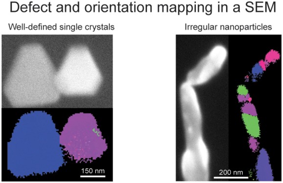
Investigating how grain structure affects the functional properties of nanoparticles requires a robust method for nanoscale grain mapping. In this study, we directly compare the grain mapping ability of transmission Kikuchi diffraction (TKD) in a scanning electron microscope to automated crystal orientation mapping (ACOM) in a transmission electron microscope across multiple nanoparticle materials. Analysis of well-defined Au, ZnO, and ZnSe nanoparticles showed that the grain orientations and GB geometries obtained by TKD are accurate and match those obtained by ACOM. For more complex polycrystalline Cu nanostructures, TKD provided an interpretable grain map whereas ACOM, with or without precession electron diffraction, yielded speckled, uninterpretable maps with orientation errors. Acquisition times for TKD were generally shorter than those for ACOM. Our results validate the use of TKD for characterizing grain orientation and grain boundary distributions in nanoparticles, providing a framework for the broader exploration of how microstructure influences nanoparticle properties.
Introduction
The underlying grain structure of nanomaterials strongly affects their functional properties. Studies of well-defined semiconducting nanowires have identified specific effects of grain orientations, phase boundaries, and defect densities on electronic, optical, thermoelectric, and (photo)electrochemical properties.1−8 A broader understanding of these phenomena across diverse semiconductor materials is crucial for the design of next-generation optical/electronic devices. Recent studies have also probed the effects of the grain structure on the catalytic properties of nanomaterials. We showed that grain boundary (GB) density is directly correlated to catalytic activity for electrochemical CO2 reduction to CO on Au nanoparticles and CO reduction to ethanol and acetate on Cu nanoparticles.9,10 GB effects have been implicated in other electrocatalytic reactions including methanol electro-oxidation on Pt nanoparticles11 and PtRu nanoparticles12 and the oxygen evolution reaction on perovskite oxides.13 GB–activity relationships in nanomaterials may arise from the accumulation of defects in the vicinity of the GB surface termination, which we have recently observed in scanning probe studies of large-grained electrodes.14 Utilizing GBs as a design element for nanoparticles in heterogeneous catalysis will require elucidating how activity depends on the GB structure.
A major bottleneck for studying these structure–function relationships is the difficulty of mapping grain structures on the nanoscale. One technique is automated crystal orientation mapping (ACOM), which is performed in a transmission electron microscope (TEM) equipped with a specialized control unit (NanoMEGAS DigiSTAR/ASTAR system).15−18 In ACOM, an electron beam is rastered across an electron-transparent sample while spot electron diffraction patterns are collected for offline analysis (Figure 1A). The patterns are indexed to a database of calculated patterns for known materials at different orientations to generate maps that show the size and orientation of the individual grains and consequently the density and geometries of the GBs. By precessing the incident electron beam around the optic axis while tilting the beam through a small angle during ACOM (a technique known as precession electron diffraction, PED), a broader range of reflections with quasi-kinematical intensities can be measured in a reciprocal space, improving the orientation indexing of collected diffraction patterns. ACOM/PED has mostly been used to obtain high-resolution maps of nanograined thin-film samples prepared by conventional TEM polishing techniques.19−21 A few recent studies have also used it to map the grain structure in discrete nanoparticles.22−24 However, it is very challenging to map structures with overlapping grains and nonuniform thickness,25−27 which are critical for studying nanoparticles used in catalysis. Moreover, the need for a TEM with specialized equipment currently limits the accessibility of ACOM/PED.
Figure 1.

Experimental schematic of ACOM/PED and TKD. (A) Microscope geometry of ACOM/PED in a TEM. (B) Microscope geometry of off-axis TKD in a SEM.
As an alternative to ACOM, Keller and Geiss recently introduced transmission Kikuchi diffraction (TKD), which is performed in a scanning electron microscope (SEM) equipped with an electron backscatter diffraction (EBSD) detector.28−31 As an electron beam is rastered across the sample, inelastic scattering within the top portion of the sample generates a divergent source of forward scattered electrons, some of which are diffracted by the bottom portion of the sample to generate Kikuchi bands. The pattern of Kikuchi bands from each spot is captured by the detector. The angles between triplets of intersecting bands in each pattern are indexed to a database of calculated interplanar angles to obtain a grain orientation, resulting in a spatially resolved orientation map for the sample (Figure 1B). In general, data acquisition is faster in TKD because of the higher signal yield from the phosphor screen to the CCD camera in an EBSD detector. Because SEMs are commonly equipped with EBSD hardware, TKD is accessible in most electron microscopy facilities, in contrast to the relatively limited accessibility of ACOM/PED.
TKD has been used to study nanograined thin films and nanoparticles.32−36 A few studies have examined the same samples using both TKD and ACOM/PED.32,37−39 However, especially for nanoparticle samples, there has not been a systematic comparison of grain orientation maps obtained by TKD versus ACOM/PED. Such a comparison is needed to illuminate key advantages and limitations of both, particularly for challenging irregular samples. In this study, we compare the grain mapping ability of ACOM/PED and TKD using well-defined Au, ZnSe, and ZnO nanoparticles and irregular, highly polycrystalline Cu nanoparticles. With well-defined nanoparticles, we show that TKD provides the same orientation and GB geometry information as ACOM. For the more complex Cu nanoparticles, we demonstrate that TKD provides an interpretable grain map, whereas ACOM yields highly speckled, uninterpretable maps. These comparisons motivate the broader utilization of TKD to investigate grain structure–function relationships in nanoparticles.
Results and Discussion
To assess nanoparticle orientation imaging with TKD, we synthesized well-defined Au nanoplates via a templated colloidal method from ∼2 nm Au nanoparticle precursors.40 Drop drying the Au nanoplates onto a Cu TEM grid backed by an ultrathin film of carbon allowed for both secondary electron (SE) and TKD imaging within a SEM. The samples were attached to a 45° SEM sample holder via a stainless steel needle (Figure S1). To minimize acquisition time for the materials studied here, we iteratively determined the minimum pattern resolutions and exposure times required for orientation indexing (Table S1). SE images of the two Au nanoplates are provided in Figure 2A,D. With an exposure time of 9.3 ms and a pixel size of 10 nm, the total acquisition time for each ∼4 μm2 map was ∼1.3–1.5 min each. TKD orientation maps of a hexagonal and a triangular Au nanoplate (AuNP-1 and AuNP-2, respectively) of ∼700–800 nm across indicated that the Au nanoplates are single crystalline and oriented along the [111] direction (Figure 2B,E, blue color, and legend in Figure 2I). Representative TKD patterns are shown in Figure 2C,F. While the surface normals of both nanoplates are oriented in the [111] direction, differences in the patterns were observed due to the sensitivity of TKD to rotations in the x–y plane (Figure S2). Because of sample drift, very small TKD pattern shifts were detected during orientation mapping and were quantified by inspection of the linear misorientation profiles obtained from the top to the bottom of the nanoplates. The slopes of the linear regression from the misorientation profiles indicated an angular drift of ∼0.002°/nm (Figure 2H). A selected area electron diffraction (SAED) pattern obtained with TEM of a single triangular 500 nm Au nanoplate confirmed that the nanoplate normal was parallel to the [111] direction (Figure 2G). These measurements corroborate earlier XRD studies showing that the as-synthesized Au nanoplates are aligned along the [111] direction.41 The match between our TKD and TEM measurements indicates that the nanoplates are truly single crystalline and that the TKD-derived orientation is accurate.
Figure 2.

TKD imaging of single-crystalline Au nanoplates. (A, B) SE and TKD images of AuNP-1. (C) TKD pattern from AuNP-1. (D, E) SE and TKD images of AuNP-2. Maps are colored according to the IPF-Z orientation. (F) TKD pattern from AuNP-2. (G) SAED pattern with inset TEM image of a single triangular Au nanoplate. (H) Linear misorientation profiles obtained from top to bottom of AuNP-1 and AuNP-2 along the inset dashed lines in (A) and (D), respectively. (I) Inverse pole figure legend for Au. (J) Illustrated real space orientations of AuNP-3 and AuNP-4. (K) SE image of AuNP-3 and AuNP-4. (L) TKD map of AuNP-3 and AuNP-4. (M, N) TKD patterns from AuNP-3 and AuNP-4.
Some caution is required when interpreting the orientations obtained by TKD. The computed orientation is directly derived from the physical alignment of the diffracting planes relative to a calibration plane (the specimen plane). Discrete nanoparticles that are aggregated will show different grain orientations if aggregation tilts one particle relative to another. To illustrate, we imaged a pair of smaller Au nanoplates (AuNP-3 and AuNP-4), with AuNP-4 lying partially atop AuNP-3. SE imaging (Figure 2K) showed that AuNP-3 and AuNP-4 are ∼400 and ∼300 nm across, respectively. Acquisition of the ∼2 μm2 TKD map at 7 nm step size required only 46 s with a 7 ms exposure time. Using AuNP-3 as the calibration area for the detector, the specimen normal direction of AuNP-3 was indexed to be very close to [111], while the specimen normal direction of AuNP-4 was close to [111] but tilted away by ∼14° (Figure 2L). The apparent misalignment from the [111] direction reflects how AuNP-4 lies atop AuNP-3 (Figure 2J) and results from a real difference in the electron beam incidence angle relative to the (111) planes in the nanoplates. Care must therefore be applied when interpreting the TKD-obtained orientations, given that nanoparticles tend to aggregate in 3D during sample preparation.
The crystallinity of metal oxide nanoparticles has previously been correlated to catalytic and electronic activity using XRD- and TEM-based analyses.42,43 To investigate if TKD could provide orientation information on discrete oxide nanoparticles, we examined zinc oxide (ZnO) nanowires grown via the thermal oxidation of an etched Zn foil at 400 °C in air.44 SE images show that the ∼5 μm-long ZnO nanowires grow vertically from a porous ZnO underlayer (Figure 3D,E and Figure S3). A sample was prepared for TKD by swiping a lacey C/Cu TEM grid over the ZnO foil immersed in isopropanol. Using a pixel size of 51 nm and exposure time of 50 ms, ∼105 μm2 TKD maps (Figure 3C,F) required ∼7.5–9.3 min of acquisition time. As ZnO is 2.4× less dense than Au, relatively long exposure times were necessary for pattern collection. TKD patterns from the ZnO nanowires exhibit Kikuchi bands with high contrast (Figure 3A,G). Along the normal direction, the ZnO nanowires were found to be aligned closely along the [0001] direction (Figure 3I), consistent with previous XRD-based studies of thermally grown ZnO films.45 The slight deviation from the [0001] direction is a consequence of the ZnO nanowire not lying perfectly flat on the substrate, similar to what was observed with AuNP-3 and AuNP-4. Certain areas bisecting the ZnO nanowires could not be indexed. In some cases, these pixels correspond to regions through which the electron beam must also pass through the lacey carbon support film on the TEM grid. Scattering by the lacey carbon support film can significantly attenuate or change the diffracted signal from the ZnO nanowire, leading to pattern misindexing (Figure 3B,H). In addition, variations in the sample thickness could also produce unindexable pixels because the diffracted signal is attenuated for thin regions.30
Figure 3.

TKD imaging of ZnO nanowires. (A, B) TKD patterns corresponding to pixels indicated by arrows in (C). (C) A TKD map of a single ZnO nanowire. Maps are colored according to the IPF-Z orientation. (D) SE image of the ZnO nanowire imaged in (C). (E, F) SE and TKD images of a second ZnO nanowire. (G, H) TKD patterns corresponding to pixels indicated by arrows in (F). (I) Inverse pole figure legend for ZnO.
The presence of GBs in semiconducting nanostructures can strongly influence charge transport, optical, and thermoelectric properties.5−7,46 To assess the GB geometries obtained by TKD, we mapped the grain structure of semiconductor ZnSe nanoribbons using both TKD and ACOM. The ZnSe nanoribbons (ZnSe-NRs) were grown on an Au/Si film via a thermal evaporation method in a H2 atmosphere.47 SE and TEM images show that the ZnSe-NRs are 300–2000 nm in diameter and 5–10 μm long and are composed of small jagged branches that grow from the central nanowire axis (Figure 4A,E and Figures S4 and S5). Previous high-resolution TEM (HRTEM) studies have found that thermally evaporated ZnSe can crystallize as flat nanoribbons either in the pure cubic zincblende phase or possess internal wurtzite/zincblende phase boundaries.48,49 Apart from pixels rendered unindexable by scattering from the underlying lacey carbon, we found that our ZnSe-NRs crystallize largely in the hexagonal wurtzite phase (Figure S4).
Figure 4.

TKD and ACOM mapping of ZnSe bi-crystalline nanoribbons. (A, B) SE and TKD images of ZnSe-NR1. (C, D) TKD patterns from individual pixels in ZnSe-NR1 indicated by inset white arrows in (B). (E, F) TEM and ACOM image of ZnSe-NR2. Inset red dashed line indicates the path for the misorientation profile in (K). Yellow circles indicate regions where speckling and misindexing were observed. (G, H) ACOM diffraction patterns from the pixels indicated by the arrows in (F). (I) Inverse pole figure orientation legend for ZnSe. (J, K) Linear misorientation profiles for ZnSe-NR1 and ZnSe-NR2 obtained across the inset dashed lines in (B) and (F), respectively.
Using a 23 nm pixel size and a total acquisition time of 8.9 min (50 ms exposure time), we obtained a ∼34 μm2 TKD map of ZnSe-NR1 that showed a single GB along its length, indicating bicrystallinity (Figure 4B). Despite occlusion from the TEM grid (causing the V-shaped pattern), TKD patterns with good contrast (Figure 4C,D) enabled indexing of the ZnSe-NR1 crystallites, with the pink and green crystallites appearing closely oriented along the [0001] and [112̅0] directions, respectively. Inspection of a linear misorientation profile across the central axis of ZnSe-NR1 showed that the GB angle is ∼65° (Figure 4J). The GB density (ρGB) calculated by dividing the GB length by the projected area is 2.44 μm–1. As seen previously in the ZnO nanowires, some unindexable points were observed in ZnSe-NR1, which may arise from interference by the lacey carbon and variations in sample thickness. Attempts to reduce the number of unindexable regions by using an ultrathin carbon support film in place of the lacey carbon were unsuccessful (Figure S5).
An ACOM map (∼0.3 μm2) of a smaller ZnSe nanoribbon (ZnSe-NR2) 150–200 nm in diameter similarly showed the nanoribbon bisected longitudinally by a single GB (Figure 4F). Images were acquired using a 3–5 nm step size and an exposure time of 30 ms. Strikingly, clear electron diffraction patterns (Figure 4G,H) showed that ZnSe-NR2 was oriented in an almost identical fashion to ZnSe-NR1, indicating excellent agreement between TKD and ACOM. A higher 2D GB surface density was obtained for ZnSe-NR2 (17.7 μm–1) as it is narrower in width. Because the obtained pattern in ACOM is highly dependent on the sample thickness, speckling and misindexing were observed at the periphery of and within ZnSe-NR2 (yellow circles, Figure 4F). Nonetheless, the consistency between ACOM and TKD in both orientation and GB geometry data (with comparable noise levels in the misorientation profiles) provides validation for the use of TKD in nanoparticle grain characterization. Consistency in the recorded GB angle and orientations was also observed when another pair of ZnSe-NRs was imaged with TKD and ACOM (Figure S6).
Cu nanomaterials are important for electronic, sensing, and catalytic applications, including the electrocatalytic conversion of CO2 and CO to multicarbon fuels. While conventional X-ray diffraction methods can be used to determine average grain sizes and texturing of polydisperse nanoparticle samples, information about the local GB geometry and GB density of individual nanoparticles is needed to unravel microstructural phenomena in detail. To evaluate the ability of TKD to map highly polycrystalline catalyst materials, we prepared oxide-derived Cu (OD-Cu) nanowires via an established two-step thermal oxidation–reduction route.50 SE images show that the Cu nanowires (CuNWs) project orthogonally away from the precursor Cu mesh and have variant lengths and thicknesses (Figure S7). Samples for TKD mapping were prepared by gently removing the nanowires from the mesh and drop-drying them onto a TEM grid. A single, 100–400 nm thick, ∼18 μm long CuNW (Cu-NW1) was first mapped using a 41 nm pixel size and 7 ms exposure time. Obtaining a ∼186 μm2 TKD map of the entire Cu-NW1 required only 1.5 min (Figure 5A and legend in Figure 5E). This low-resolution map shows 66 individual grains in Cu-NW1 with an average grain size of 0.18 μm and a broad size distribution (Figure 5C). Inverse pole figures (Figure 5B) show that in the Z direction, large portions of the grains are oriented parallel to the [111] direction in this particular nanowire. The distribution of grain boundary misorientations showed a large number of GBs oriented close to 60° (likely corresponding to twin GBs) and a second maximum of low-angle GBs (Figure 5D).
Figure 5.

Comprehensive TKD characterization of Cu-NW1. (A) TKD map of Cu-NW1. Inset is the corresponding SE image with locations of TKD maps in (F) through (H) marked. (B) Inverse pole figures of Cu-NW1 along the X, Y, and Z directions. Each pixel corresponds to a unique diffraction pattern from the TKD map in (A). (C) Grain size distribution derived from (A). (D) Grain boundary misorientation distribution derived from (A). (E) Inverse pole figure legend for Cu. (F–H) TKD maps and calculated GB densities (ρGB) of Cu-NW1a-c. Maps are colored according to the IPF-Z orientation.
To probe the grain structure of Cu-NW1 on the nanoscale and quantify ρGB, orientation maps were collected along the length using a pixel size of ∼9 nm and a 7 ms exposure time (labeled as Cu-NW1a-c in Figure 5F–H). Each ∼4–10 μm2 map required only ∼1–1.5 min. Approximately 85% of the GBs in Cu-NW1 were found to be coincident site lattice (CSL) GBs, with 92% of those CSL GBs adopting Σ3<111>60° twin geometry, corroborating the GB misorientation distribution of the whole wire. The high-magnification mapping also revealed that 5% of the CSL GBs adopted the Σ9<110>39° geometry. The ρGB calculated from the TKD maps of Cu-NW1a-c was similar, with an average of 7.2 ± 0.6 μm–1. Because of the mechanism of TKD pattern generation (Figure 1B), the presence of multiple crystallites through thick regions of the NW either results in unindexable regions with no distinct Kikuchi bands or identification of only the bottommost crystallite of the NW. The ρGB values are therefore lower bounds that represent the value for a particle in which there is only one grain in the interaction volume for each pixel.
To assess the mapping ability on smaller length scales, TKD maps of CuNWs that were 30–50 nm thick and 200–1500 nm in length (Cu-NW2 through CuNW4) were obtained using 2.5–5 nm pixel sizes. The 0.7–7 μm2 maps were obtained in 3–5 min (Figure 6A–C and example patterns in Figure 6D,E and Figure S8). In contrast to Cu-NW1, Cu-NW2 through Cu-NW4 displayed no distinct texture, indicating a large diversity in orientation across the NWs present in OD-Cu. Local misorientation profiles (Figure 6K,L) across Cu-NW3 and Cu-NW4 show that the grains are 25–100 nm across. Local misorientation analysis also yielded insight into GB geometry. A small ∼20 nm twin domain terminated by a pair of Σ3<111>60° GBs was detected in Cu-NW3, in addition to a ∼23° GB at the tip of the NW (yellow circles in Figure 6B,C). A much larger 75 nm twin domain was observed in the middle of Cu-NW4. The ρGB values were calculated to be 9.7, 16.3, and 13.1 μm–1 for Cu-NW2, Cu-NW3, Cu-NW4, respectively. These values were somewhat higher than Cu-NW1, indicating substantial variance in the degree of polycrystallinity between individual OD-Cu nanowires.
Figure 6.

TKD and ACOM imaging of highly polycrystalline OD-Cu nanowires. (A–C) TKD images of Cu-NW2, Cu-NW3, and Cu-NW4. Yellow circles indicate location of twin domains. (D, E) Example TKD patterns from Cu-NW4. Inset red crosses mark the pattern centers. (F–H) ACOM images of Cu-NW5, Cu-NW6, and Cu-NW7. (I, J) Diffraction patterns from Cu-NW7 at the pixels indicated by the arrows in (H). The inset boxes indicate the portions of the electron diffraction patterns that result in a calculated misorientation between the two pixels. (K, L) Linear misorientation profiles obtained from the dashed lines in TKD maps (B) and (C). (M, N) Linear misorientation profiles obtained from the dashed lines in (G) and (H).
Using ACOM, isolated OD-Cu nanowires were imaged using a probe size of 5 nm and exposure time of ∼40 ms (Figure 6F–H and image quality maps in Figure S9). As seen in the TKD maps, the Cu NWs appear highly polycrystalline, with 25–100 nm grains, and have no preferred orientation. In contrast to the TKD maps, speckling was observed in the ACOM maps; regions of different thicknesses within the same grain were indexed to different orientations. For instance, the orientation profile within a large crystallite in NW7 (Figure 6H, tan grain) fluctuated by ∼15° over the length of the grain (Figure 6N). Example diffraction patterns from adjacent regions of the tan grain (Figure 6I,J) show that the appearance of minor reflections in some of the pixels led to pattern misindexing. Unlike the misorientation profiles obtained with TKD (Figure 6K,L), the profiles obtained with ACOM across NW6 and NW7 (Figure 6M,N) suggest that the detected patterns in these regions are generated by more than one grain in the interaction volume.
For most applications of orientation mapping in nanocrystalline specimens, PED provides more accurate orientation indexing than ACOM because precessing the beam reveals more of the reciprocal space during acquisition. To assess how TKD would compare to state-of-the-art PED techniques, we collected additional PED maps of an identically prepared Cu nanowire (Cu-NW8) using a precession angle of 0.7°, 4 nm step size, and an exposure time of 40 ms (Figure S10A,B). Comparison of the maps collected with and without precession (Figure S10C,D) showed that orientation indexing in regions of Cu-NW8 with nonuniform thickness remained ambiguous. Large variations in the misorientation profiles within the grain interiors were observed (Figure S10E,F). For Cu NWs with uneven thicknesses, scattering from multiple grains during ACOM or PED acquisition renders the resulting orientation maps difficult to interpret.32 Consequently, it was not possible to compute even lower-bound ρGB or a misorientation distribution with the ACOM/PED system because the presence of GBs could not be assigned with confidence in the speckled regions. Within a portion of a nanowire of an uneven thickness, PED could be employed to obtain GB distributions by acquiring a tilt series of the grain, although obtaining quantitative GB densities for a highly heterogeneous ensemble would be very laborious.51
Even with state-of-the-art subtracting-indexing algorithms, resolved, planar 2D maps of the grain structure in nanostructures with multiple overlapping grains remain inaccessible with ACOM/PED, leading to diminished sensitivity to surface structural features relative to TKD.26 In contrast, the majority of the diffracted electrons in TKD come from the grains at the bottom of the sample.31,52 In vertical sections with two or more grains, the pattern will likely be of the bottommost grain or appear unindexable. Thus, for irregular, polycrystalline nanoparticles, TKD provides a simplified orientation map of surface-exposed grains, which enables quantification of lower-bound estimates of ρGB and GB geometry distributions that cannot be obtained with ACOM/PED.
The ability to rapidly map the nanoparticle grain structure provides a basis for a more thorough investigation of microstructural effects on catalysis. For electrocatalysis in particular, recent advances in scanning probe microscopy enable spatially resolved measurements of catalytic activity with 10 nm resolution.53,54 Combining these measurements with TKD mapping could illuminate the contributions of the grain structure to the activity in nanoparticle electrocatalysts. More broadly, rapid characterization of the nanoparticle grain structure could be used to establish robust correlations between grain orientation, ρGB, and GB geometries for many catalytic processes.
Conclusions
In summary, our studies demonstrate the advantages of TKD for orientation imaging and GB characterization of nanoparticles and nanowires. TKD provides an accurate grain map that is in agreement with the results of TEM-based diffraction techniques, as demonstrated by the analysis of well-defined nanostructures. Furthermore, TKD is uniquely capable of providing an interpretable grain map of highly polycrystalline nanoparticles and samples with uneven thickness, characteristics that are common in catalytic and other functional materials. These features, combined with the wide accessibility, short acquisition times, and low cost of SEM-based imaging techniques, motivate the broad use of TKD for quantitative investigations into how grain structure influences functional properties. The off-axis TKD methods used here are suitable for mapping nanoparticles with dimensions on the order of tens of nanometer or greater. However, the use of both improved detectors and on-axis TKD with low probe currents could further decrease pixel sizes below 2 nm, allowing for diffractive mapping of smaller and/or finer-grained samples.55,56
Experimental Section
Materials
Cu TEM grids (300 mesh) with 15–25 nm ultrathin carbon film on lacey carbon support film, 300 mesh Cu TEM grids with lacey carbon support film, 400 mesh Au TEM grids with 15–25 nm ultrathin carbon film, 30 nm Si3N4/Si TEM grids, Si imaging substrates, a 45° pretilt SEM holder, silver paint, and a needle clamp were all obtained from Ted Pella. N-type Si(100) single crystal wafers were obtained from University Wafer. HCl and HNO3 were obtained from Fisher. Sodium tetrachloroaurate(III) dihydrate (99%) and Zn foil (0.5 mm thick, 99.9%) were obtained from Alfa Aesar. Sodium citrate, cetyltrimethylammonium bromide (CTAB, 95%), and ZnSe (99.99%) were obtained from Sigma-Aldrich. Cu mesh (99.9%) was obtained from McMaster Carr.
Material Synthesis
Au nanoplates were synthesized using an adapted templated colloidal method.57 Fifteen milligrams of sodium citrate was dissolved in 30 mL of DI H2O and heated to 50 °C in a glass vial. A second solution of 9.0 mg of NaAuCl4·2H2O and 55 mg of CTAB in 20 mL of DI H2O was heated to 50 °C in a glass vial and added to the citrate solution while stirring. The mixture was then heated at 82 °C for 20 min after which the nanoplates precipitate as orange solids. For purification and removal of the excess CTAB template, 50 mL of mixture was centrifuged at 4000 rpm for 30 min. The supernatant was drained, and the solids were resuspended in 50 mL of DI water, followed by a second centrifugation at 4000 rpm for 30 min and resuspension in 5 mL of DI water to obtain Au nanoplates suspended in H2O.
ZnO nanowire arrays were grown by annealing Zn foil.44 Prior to use, the Zn foil was etched in 10% w/w HCl solution for 30 s, followed by thorough rinsing in deionized (DI) water. The etched Zn foil was then heated in air within a box furnace at 400 °C for 1 h, followed by ambient cooling to room temperature overnight.
ZnSe was prepared by an adapted thermal evaporation method.47 ZnSe powder (0.25 g) was placed in a quartz boat in the middle of a quartz tube in a tube furnace, while Si(100) chips coated with 25 nm of Au (deposited at 0.2 nm/s within a Kurt J. Lesker evaporator) were placed approximately 15 cm downstream. The tube was evacuated with house vacuum for 5 min, placed under 1 atm of 100% H2 flowing at 200 sccm, and heated to 950 °C for 2 h.
CuO nanowire arrays were grown by annealing Cu mesh. Prior to use, the Cu mesh was etched in 10% w/w HNO3 for 60 s, followed by rinsing with DI water. The etched Cu mesh was then heated in air within a box furnace at 500 °C for 1 h, followed by ambient cooling to room temperature overnight.50 CuNW arrays were made via the thermal reduction of the CuO nanowire arrays in 1 atm of H2 flowing at 100 sccm for 2 h at 200 °C.
Characterization
Samples were loaded onto Cu TEM grids for both SEM/TKD and TEM/ACOM imaging. SEM imaging was performed on an FEI Magellan 400 XHR SEM equipped with a Bruker eFlash-HR detector and a UHR stage. Acquisition and analysis of TKD data were performed with Esprit 2.1. The EBSD detector was mounted at ∼10.5° detector tilt. Images were acquired at 20° sample tilt using the TKD holder (Figure S1). Brandon’s criterion (Δθ = 15° Σ–1/2)58 was used to classify GBs according to CSL notation.
PED and ACOM-TEM imaging and analysis were performed at Lawrence Livermore National Laboratory using a Philips CM300 TEM equipped with the ASTAR/DigiSTAR/TopSpin precession electron diffraction (PED) orientation mapping system (equipped with a StingRay F046B camera) from NanoMEGAS. The probe spot size was on the order of ∼5 nm. For PED acquisition, four precessions/pixels and a precession angle of 0.7° were used. Contrast in the ACOM diffraction patterns shown in Figures 4 and 6 was enhanced for clarity in the figures but not for analysis.
For TKD analysis, a blunt 1.8 cm 22-gauge needle cut from a standard stainless steel needle was dipped in Ag epoxy and touched to the TEM grid loaded with the sample to make contact. A small amount of Ag epoxy was applied to the back using a second stainless steel needle. The assembly was allowed to cure at 80 °C in a box furnace for ∼30 min. To image CuNWs, the grid was Ag epoxied to the needle and cured before the samples were drop dried because of the air sensitivity of Cu. The needle was carefully clamped onto a needle holder (Ted Pella no. 15290) with a set screw, and the whole assembly was then mounted onto a 45° 12.7 mm PELCO SEM holder for EBSD (Ted Pella no. 15329). The needle holder was rotated until the surface of the mounted Cu grid faced upward to minimize the number of scattered electrons that landed onto the Cu grid on the way to the detector. Cu nanowire samples were prepared for TEM imaging by swirling the Cu nanowire array in deaerated IPA, following by drop drying onto TEM grids. ZnSe and ZnO nanowire samples were collected for imaging by placing a small piece of the product substrate in a Petri dish with IPA, swiping the TEM grid across the sample, and allowing the grid to dry on filter paper. During imaging, the lowest possible detector resolution and acquisition times were iteratively determined. The detector was calibrated on a small area containing the nanostructure to be imaged and in some cases may not correspond perfectly to the true microscope normal. Usage of low acquisition times reduced drift during map acquisition, which generally improved the fidelity of the TKD maps to the SE image taken just before mapping. TKD images have been cropped for clarity to exclude background images of SEM vacuum or carbon support. The total acquisition times, map sizes, and pixel counts refer to the entire uncropped image.
Acknowledgments
Work at Lawrence Livermore National Laboratory was performed under the auspices of the U.S. Department of Energy under Contract no. DE-AC52-07NA27344. Work at Stanford was supported by the NSF (CHE-1565945). R.G.M. gratefully acknowledges the NSF for a Pre-Doctoral Fellowship and Stanford University for a DARE fellowship. EBSD and TEM were performed at the Stanford Nano Shared Facilities (SNSF), which is supported by the National Science Foundation under award ECCS-1542152.
Supporting Information Available
The Supporting Information is available free of charge at https://pubs.acs.org/doi/10.1021/acsomega.9b03505.
Supplementary tables, photos, electron microscopy images, and diffraction data (PDF)
The authors declare no competing financial interest.
Supplementary Material
References
- Dayeh S. A. Electron transport in indium arsenide nanowires. Semicond. Sci. Technol. 2010, 25, 024004 10.1088/0268-1242/25/2/024004. [DOI] [Google Scholar]
- Thelander C.; Caroff P.; Plissard S.; Dey A. W.; Dick K. A. Effects of crystal phase mixing on the electrical properties of InAs nanowires. Nano Lett. 2011, 11, 2424–2429. 10.1021/nl2008339. [DOI] [PubMed] [Google Scholar]
- Mårsell E.; Boström E.; Harth A.; Losquin A.; Guo C.; Cheng Y.-C.; Lorek E.; Lehmann S.; Nylund G.; Stankovski M.; Arnold C. L.; Miranda M.; Dick K. A.; Mauritsson J.; Verdozzi C.; L’Huillier A.; Mikkelsen A. Spatial Control of Multiphoton Electron Excitations in InAs Nanowires by Varying Crystal Phase and Light Polarization. Nano Lett. 2018, 18, 907–915. 10.1021/acs.nanolett.7b04267. [DOI] [PubMed] [Google Scholar]
- Kuykendall T. R.; Altoe M. V. P.; Ogletree D. F.; Aloni S. Catalyst-Directed Crystallographic Orientation Control of GaN Nanowire Growth. Nano Lett. 2014, 14, 6767–6773. 10.1021/nl502079v. [DOI] [PubMed] [Google Scholar]
- Amit I.; Englander D.; Horvitz D.; Sasson Y.; Rosenwaks Y. Density and Energy Distribution of Interface States in the Grain Boundaries of Polysilicon Nanowire. Nano Lett. 2014, 14, 6190–6194. 10.1021/nl5024468. [DOI] [PubMed] [Google Scholar]
- Baxter J. B.; Schmuttenmaer C. A. Conductivity of ZnO Nanowires, Nanoparticles, and Thin Films Using Time-Resolved Terahertz Spectroscopy. J. Phys. Chem. B 2006, 110, 25229–25239. 10.1021/jp064399a. [DOI] [PubMed] [Google Scholar]
- Li J.-F.; Liu W.-S.; Zhao L.-D.; Zhou M. High-performance nanostructured thermoelectric materials. NPG Asia Mater. 2010, 2, 152–158. 10.1038/asiamat.2010.138. [DOI] [Google Scholar]
- Hou W.; Cortez P.; Wuhrer R.; Macartney S.; Bozhilov K. N.; Liu R.; Sheppard L. R.; Kisailus D. Oriented epitaxial TiO2 nanowires for water splitting. Nanotechnology 2017, 28, 265602. 10.1088/1361-6528/aa7356. [DOI] [PubMed] [Google Scholar]
- Feng X.; Jiang K.; Fan S.; Kanan M. W. Grain-Boundary-Dependent CO2 Electroreduction Activity. J. Am. Chem. Soc. 2015, 137, 4606–4609. 10.1021/ja5130513. [DOI] [PubMed] [Google Scholar]
- Feng X.; Jiang K.; Fan S.; Kanan M. W. A Direct Grain-Boundary-Activity Correlation for CO Electroreduction on Cu Nanoparticles. ACS Cent. Sci. 2016, 2, 169–174. 10.1021/acscentsci.6b00022. [DOI] [PMC free article] [PubMed] [Google Scholar]
- Wang S.; Jiang S. P.; White T. J.; Guo J.; Wang X. Electrocatalytic Activity and Interconnectivity of Pt Nanoparticles on Multiwalled Carbon Nanotubes for Fuel Cells. J. Phys. Chem. C 2009, 113, 18935–18945. 10.1021/jp906923z. [DOI] [Google Scholar]
- Gavrilov A. N.; Savinova E. R.; Simonov P. A.; Zaikovskii V. I.; Cherepanova S. V.; Tsirlina G. A.; Parmon V. N. On the influence of the metal loading on the structure of carbon-supported PtRu catalysts and their electrocatalytic activities in CO and methanol electrooxidation. Phys. Chem. Chem. Phys. 2007, 9, 5476–5489. 10.1039/b707598g. [DOI] [PubMed] [Google Scholar]
- Heo Y.; Choi S.; Bak J.; Kim H.-S.; Bae H. B.; Chung S.-Y. Symmetry-Broken Atom Configurations at Grain Boundaries and Oxygen Evolution Electrocatalysis in Perovskite Oxides. Adv. Energy Mater. 2018, 8, 1802481. 10.1002/aenm.201802481. [DOI] [Google Scholar]
- Mariano R. G.; McKelvey K.; White H. S.; Kanan M. W. Selective increase in CO2 electroreduction activity at grain-boundary surface terminations. Science 2017, 358, 1187–1192. 10.1126/science.aao3691. [DOI] [PubMed] [Google Scholar]
- Rauch E. F.; Veron M. Coupled microstructural observations and local texture measurements with an automated crystallographic orientation mapping tool attached to a TEM. Materialwiss. Werkstofftech. 2005, 36, 552–556. 10.1002/mawe.200500923. [DOI] [Google Scholar]
- Rauch E. F.; Véron M. Automated crystal orientation and phase mapping in TEM. Mater. Charact. 2014, 98, 1–9. 10.1016/j.matchar.2014.08.010. [DOI] [Google Scholar]
- Viladot D.; Véron M.; Gemmi M.; Peiró F.; Portillo J.; Estradé S.; Mendoza J.; Llorca-Isern N.; Nicolopoulos S. Orientation and phase mapping in the transmission electron microscope using precession-assisted diffraction spot recognition: state-of-the-art results. J. Microsc. 2013, 252, 23–34. 10.1111/jmi.12065. [DOI] [PubMed] [Google Scholar]
- Morawiec A.; Bouzy E.; Paul H.; Fundenberger J. J. Orientation precision of TEM-based orientation mapping techniques. Ultramicroscopy 2014, 136, 107–118. 10.1016/j.ultramic.2013.08.008. [DOI] [PubMed] [Google Scholar]
- Ghamarian I.; Samimi P.; Telang A.; Vasudevan V. K.; Collins P. C. Characterization of the near-surface nanocrystalline microstructure of ultrasonically treated Ti-6Al-4V using ASTARTM/precession electron diffraction technique. Mater. Sci. Eng.: A 2017, 688, 524–531. 10.1016/j.msea.2017.02.029. [DOI] [Google Scholar]
- Sun F.; Zhang J. Y.; Marteleur M.; Brozek C.; Rauch E. F.; Veron M.; Vermaut P.; Jacques P. J.; Prima F. A new titanium alloy with a combination of high strength, high strain hardening and improved ductility. Scr. Mater. 2015, 94, 17–20. 10.1016/j.scriptamat.2014.09.005. [DOI] [Google Scholar]
- Lilensten L.; Couzinié J. P.; Perriëre L.; Bourgon J.; Emery N.; Guillot I. New structure in refractory high-entropy alloys. Mater. Lett. 2014, 132, 123–125. 10.1016/j.matlet.2014.06.064. [DOI] [Google Scholar]
- Consonni V.; Rapenne L.; Renou G.; Roussel H.; Gérard L.; Cuscó R.; Artús L.; André R.; Rauch E. F. Identifying and mapping the polytypes and orientation relationships in ZnO/CdSe core–shell nanowire arrays. Nanotechnology 2016, 27, 445712. 10.1088/0957-4484/27/44/445712. [DOI] [PubMed] [Google Scholar]
- Santiago U.; Velázquez-Salazar J. J.; Sanchez J. E.; Ruiz-Zepeda F.; Ortega J. E.; Reyes-Gasga J.; Bazán-Díaz L.; Betancourt I.; Rauch E. F.; Veron M.; Ponce A.; José-Yacamán M. A stable multiply twinned decahedral gold nanoparticle with a barrel-like shape. Surf. Sci. 2016, 644, 80–85. 10.1016/j.susc.2015.09.015. [DOI] [Google Scholar]
- Robert D.; Douillard T.; Boulineau A.; Brunetti G.; Nowakowski P.; Venet D.; Bayle-Guillemaud P.; Cayron C. Multiscale Phase Mapping of LiFePO4-Based Electrodes by Transmission Electron Microscopy and Electron Forward Scattering Diffraction. ACS Nano 2013, 7, 10887–10894. 10.1021/nn4043964. [DOI] [PubMed] [Google Scholar]
- Valery A.; Rauch E. F.; Pofelski A.; Clement L.; Lorut F. Dealing With Multiple Grains in TEM Lamellae Thickness for Microstructure Analysis Using Scanning Precession Electron Diffraction. Microsc. Microanal. 2015, 21, 1243–1244. 10.1017/S143192761500700X. [DOI] [Google Scholar]
- Valery A.; Rauch E. F.; Clément L.; Lorut F. Retrieving overlapping crystals information from TEM nano-beam electron diffraction patterns. J. Microsc. 2017, 268, 208–218. 10.1111/jmi.12599. [DOI] [PubMed] [Google Scholar]
- Sun B. B.; Wang Y. B.; Wen J.; Yang H.; Sui M. L.; Wang J. Q.; Ma E. Artifacts induced in metallic glasses during TEM sample preparation. Scr. Mater. 2005, 53, 805–809. 10.1016/j.scriptamat.2005.06.007. [DOI] [Google Scholar]
- Keller R. R.; Geiss R. H. Transmission EBSD from 10 nm domains in a scanning electron microscope. J. Microsc. 2012, 245, 245–251. 10.1111/j.1365-2818.2011.03566.x. [DOI] [Google Scholar]
- Geiss R. H.; Rice K. P.; Keller R. R. Transmission EBSD in the scanning electron microscope. Micros. Today 2013, 21, 16–20. 10.1017/S1551929513000503. [DOI] [Google Scholar]
- Rice K. P.; Keller R. R.; Stoykovich M. P. Specimen-thickness effects on transmission Kikuchi patterns in the scanning electron microscope. J. Microsc. 2014, 254, 129–136. 10.1111/jmi.12124. [DOI] [PubMed] [Google Scholar]
- Trimby P. W. Orientation mapping of nanostructured materials using transmission Kikuchi diffraction in the scanning electron microscope. Ultramicroscopy 2012, 120, 16–24. 10.1016/j.ultramic.2012.06.004. [DOI] [PubMed] [Google Scholar]
- Abbasi M.; Kim D.-I.; Guim H.-U.; Hosseini M.; Danesh-Manesh H.; Abbasi M. Application of transmitted Kikuchi diffraction in studying nano-oxide and ultrafine metallic grains. ACS Nano 2015, 9, 10991–11002. 10.1021/acsnano.5b04296. [DOI] [PubMed] [Google Scholar]
- Alekseeva S.; da Silva Fanta A. B.; Iandolo B.; Antosiewicz T. J.; Nugroho F. A. A.; Wagner J. B.; Burrows A.; Zhdanov V. P.; Langhammer C. Grain boundary mediated hydriding phase transformations in individual polycrystalline metal nanoparticles. Nat. Commun. 2017, 8, 1084. 10.1038/s41467-017-00879-9. [DOI] [PMC free article] [PubMed] [Google Scholar]
- Wang K.; Doerner R. P.; Baldwin M. J.; Meyer F. W.; Bannister M. E.; Darbal A.; Stroud R.; Parish C. M. Morphologies of tungsten nanotendrils grown under helium exposure. Sci. Rep. 2017, 7, 42315. 10.1038/srep42315. [DOI] [PMC free article] [PubMed] [Google Scholar]
- Parish C. M.; Wang K.; Doerner R. P.; Baldwin M. J. Grain orientations and grain boundaries in tungsten nonotendril fuzz grown under divertor-like conditions. Scr. Mater. 2017, 127, 132–135. 10.1016/j.scriptamat.2016.09.018. [DOI] [Google Scholar]
- Wollschläger N.; Palasse L.; Häusler I.; Dirscherl K.; Oswald F.; Narbey S.; Ortel E.; Hodoroaba V.-D. Characterization of the inner structure of porous TiO2 nanoparticle films in dye sensitive solar cells (DSSC) by focused ion beam (FIB) tomography and transmission Kikuchi diffraction (TKD) in the scanning electron microscope (SEM). Mater. Charact. 2017, 131, 39–48. 10.1016/j.matchar.2017.06.030. [DOI] [Google Scholar]
- Geiss R. H. Correlation of Electron Diffraction between t-EBSD in the SEM, CBED in the TEM and ACOM using ASTAR in the TEM using GaN Nanowires. Microsc. Microanal. 2015, 21, 1249–1250. 10.1017/S1431927615007035.26315895 [DOI] [Google Scholar]
- Stuckert E. P.; Geiss R. H.; Miller C. J.; Fisher E. R. In-Depth View of the Structure and Growth of SnO2 Nanowires and Nanobrushes. ACS Appl. Mater. Interfaces 2016, 8, 22345–22353. 10.1021/acsami.6b06676. [DOI] [PubMed] [Google Scholar]
- Liu T.; Leazer J. D.; Brewer L. N. Deformation Microstructures in Individual Cold Sprayed Al-Cu Alloy Particles Studied via Precession Electron Diffraction and Transmission Kikuchi Diffraction. Microsc. Microanal 2018, 24, 2180–2181. 10.1017/S1431927618011388. [DOI] [Google Scholar]
- Ni Y.; Kan C.; Xu J.; Liu Y. The synthesis of high yield Au nanoplate and optimized optical properties. Superlattices Microstruct. 2018, 114, 124–142. 10.1016/j.spmi.2017.12.021. [DOI] [Google Scholar]
- Hong S.; Acapulco J. A. I. Jr.; Jang H.-J.; Kulkarni A. S.; Park S. Kinetically controlled growth of gold nanoplates and nanorods via a one-step seed-mediated method. Bull. Korean Chem. Soc 2014, 35, 1737–1742. 10.5012/bkcs.2014.35.6.1737. [DOI] [Google Scholar]
- Jiang K.; Wang H.; Cai W.-B.; Wang H. Li Electrochemical Tuning of Metal Oxide for Highly Selective CO2 Reduction. ACS Nano 2017, 11, 6451–6458. 10.1021/acsnano.7b03029. [DOI] [PubMed] [Google Scholar]
- Senthamizhan A.; Balusamy B.; Aytac Z.; Uyar T. Grain boundary engineering in electrospun ZnO nanostructures as promising photocatalysts. CrystEngComm 2016, 18, 6341–6351. 10.1039/C6CE00693K. [DOI] [Google Scholar]
- Tan W. K.; Razak K. A.; Ibrahim K.; Lockman Z. Oxidation of etched Zn foil for the formation of ZnO nanostructure. J. Alloys Compd. 2011, 509, 6806–6811. 10.1016/j.jallcom.2011.03.055. [DOI] [Google Scholar]
- Kong X. Y.; Wang Z. L. Spontaneous polarization-induced nanohelixes, nanosprings, and nanorings of piezoelectric nanobelts. Nano Lett. 2003, 3, 1625–1631. 10.1021/nl034463p. [DOI] [Google Scholar]
- Sanchez A. M.; Zhang Y.; Tait E. W.; Hine N. D. M.; Liu H.; Beanland R. Nonradiative Step Facets in Semiconductor Nanowires. Nano Lett. 2017, 17, 2454–2459. 10.1021/acs.nanolett.7b00123. [DOI] [PubMed] [Google Scholar]
- Jin L.; Wang J.; Cao G.; Xu Z.; Jia S.; Choy W. C. H.; Leung Y. P.; Yuk T. I. {113} twinned ZnSe bicrystal nanobelts filled with < 111 > twinnings. J. Phys. Chem. C 2008, 112, 4903–4907. 10.1021/jp710800w. [DOI] [Google Scholar]
- Wang Y. Q.; Philipose U.; Ruda H.; Kavanagh K. L. Planar defects and phase transformation in ZnSe nanosaws. J. Mater. Sci.: Mater. Electron. 2006, 17, 1065–1070. 10.1007/s10854-006-9006-6. [DOI] [Google Scholar]
- Jin L.; Wang J.; Jia S.; Jiang Q.; Yan X.; Lu P.; Cai Y.; Deng L.; Choy W. C. H. ZnSe Heterocrystalline Junctions Based on Zinc Blende–Wurtzite Polytypism. J. Phys. Chem. C 2010, 114, 1411–1415. 10.1021/jp909182e. [DOI] [Google Scholar]
- Li C. W.; Ciston J.; Kanan M. W. Electroreduction of carbon monoxide to liquid fuel on oxide-derived nanocrystalline copper. Nature 2014, 508, 504–507. 10.1038/nature13249. [DOI] [PubMed] [Google Scholar]
- Eggeman A. S.; Krakow R.; Midgley P. A. Scanning precession electron tomography for three-dimensional nanoscale orientation imaging and crystallographic analysis. Nat. Commun. 2015, 6, 7267. 10.1038/ncomms8267. [DOI] [PMC free article] [PubMed] [Google Scholar]
- Liu J.; Lozano-Perez S.; Wilkinson A. J.; Grovenor C. R. M. On the depth resolution of transmission Kikuchi diffraction (TKD) analysis. Ultramicroscopy 2019, 205, 5–12. 10.1016/j.ultramic.2019.06.003. [DOI] [PubMed] [Google Scholar]
- Bentley C. L.; Kang M.; Unwin P. R. Nanoscale Structure Dynamics within Electrocatalytic Materials. J. Am. Chem. Soc. 2017, 139, 16813–16821. 10.1021/jacs.7b09355. [DOI] [PubMed] [Google Scholar]
- Bentley C. L.; Unwin P. R. Nanoscale Electrochemical Movies and Synchronous Topographical Mapping of Electrocatalytic Materials. Faraday Discuss. 2018, 210, 365–379. 10.1039/C8FD00028J. [DOI] [PubMed] [Google Scholar]
- Vespucci S.; Winkelmann A.; Mingard K.; Maneuski D.; O’Shea V.; Trager-Cowan C. Exploring transmission Kikuchi diffraction using a Timepix detector. J. Instrum. 2017, 12, C02075. 10.1088/1748-0221/12/02/C02075. [DOI] [Google Scholar]
- Niessen F.; Burrows A.; Fanta A. B. d. S. A systematic comparison of on-axis and off-axis transmission Kikuchi diffraction. Ultramicroscopy 2018, 186, 158–170. 10.1016/j.ultramic.2017.12.017. [DOI] [PubMed] [Google Scholar]
- Deckert-Gaudig T.; Deckert V. Ultraflat Transparent Gold Nanoplates - Ideal Substrates for Tip-enhanced Raman Scattering Experiments. Small 2009, 5, 432–436. 10.1002/smll.200801237. [DOI] [PubMed] [Google Scholar]
- Brandon D. G. The structure of high-angle grain boundaries. Acta Metall. 1966, 14, 1479–1484. 10.1016/0001-6160(66)90168-4. [DOI] [Google Scholar]
Associated Data
This section collects any data citations, data availability statements, or supplementary materials included in this article.