

Abstract
This mini review focuses on the effect of preparation technologies on the piezoelectric property of KNN-based materials. The piezoelectric properties of KNN-based ceramics can be optimized by controlling the condition for sintering and poling processes. The preparation method of textured and single crystals could realize an increased piezoelectric constant compared to that of corresponding ceramics. According to current developments in preparation technology, we also provide perspectives and outlooks of lead-free KNN-based materials.
1. Introduction
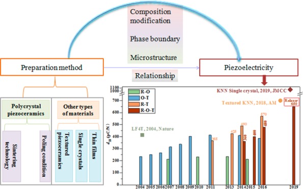
Among the alternatives replacing lead-based piezomaterials, KNN-based materials have been considered as one of the most promising candidates to replace the lead-based ones due to a large piezoelectric constant (d33) and high Curie temperature. In general, chemical modification (e.g., Li+, Ba2+, Sb5+, Ta5+, CaZrO3, Bi0.5Na0.5ZrO3, SrTiO3, etc.) and new phase boundary construction [e.g., rhombohedral–orthorhombic–tetragonal (R–O–T), rhombohedral–tetragonal (R–T), etc.] have been employed.1 As shown in Figure 1, the ceramics with O–T phase boundary are first investigated, and the ceramics with the R–O phase boundary have a relatively low d33. Interestingly, the d33 can be promoted by constructing new R–T or R–O–T phase boundaries. For example, a large d33 of 570 pC/N by constructing the R–T phase boundary can be obtained due to the coexistence of nanoscale domains (1–2 nm) and a high density of ferroelectric domain boundaries.2 A higher d33 of 650 pC/N by forming a relaxor R–O–T phase boundary was reported in 2019, which is the highest value in reported work so far in nontextured KNN-based ceramics.2 However, the d33 of KNN-based ceramics can be maximized only by optimizing the sintering and poling conditions. In addition, the reaction template grain growth (RTGG) can further promote the d33 of KNN-based ceramics.3 Improvement of electrical properties can be also obtained in KNN-based single crystals and/or thin films by optimizing the preparation technologies.4,5
Figure 1.

Evolution of d33 in KNN-based materials varying with time.1−4,6
In this mini review, the progress in preparation technologies for KNN-based materials is summarized and discussed, and the effect of preparation technologies on the piezoelectricity of KNN-based polycrystalline ceramics is highlighted. In addition, we also summarize the factors affecting the piezoelectric constant of textured ceramics, single crystals, and thin films.
2. Polycrystalline KNN-Based Ceramics
Sintering technology could affect the phase structure and microstructure (e.g., grain size, point defect, domain structure) of KNN-based ceramics. Some sintering methods can enhance piezoelectricity, including two-step sintering, spark-plasma sintering, hot-press sintering, etc. In addition, sintering aid, sintering temperature and atmosphere, and poling condition also influence the piezoelectricity of polycrystalline ceramics.
2.1. Sintering Methods
Some sintering methods have been used to increase the sinterability of KNN-based ceramics, including conventional sintering (CS), multistep sintering, spark-plasma sintering (SPS), hot-press sintering (HPS), microwave sintering (MS), etc. Subsequently, we systematically review the development of three kinds of sintering technologies which have been widely used in the sintering process for fabricating KNN-based ceramics.
2.1.1. Multistep Sintering
The samples were heated to a high temperature and held for a long time in the CS process. The rapid grain growth that has a serious impact on the density and piezoelectricity of the ceramics would occur in the CS method, which can be inhibited by a two-step sintering (TSS) method using different kinetics between grain boundary diffusion and grain boundary migration. In the TSS process, the samples were heated to a higher temperature (T1) and held for a short time (t1) to achieve an intermediate density and then cooled to a lower temperature (T2) and held for a long time (t2) to achieve the maximum density without final-stage grain growth. High d33 (350–400 pC/N) over a wide sintering temperature range (400–1050 °C) can be found in KNN-based ceramics with R–T coexistence phases and dense microstructure without heavy loss of alkali elements by the TSS method.7 In 2019, a high d33 of 455 pC/N was realized due to the quite uniform grain size distribution and parallel domain stripes with hierarchical nanodomain structure, which were prepared by TSS with a tailed dwelling time in the second step.8 In addition, considering the issues in two-step sintering in which the volatility of alkali elements occurred because of the relatively high T1 in the first step and a quite long dwelling time in the second step, a high density value (97.5%) and an increased d33 (436 pC/N) can be obtained in KNLNTS ceramics using a modified TSS.9 Furthermore, the improved d33 of 420 pC/N can be achieved in KNLNS-CaZrO3 ceramics with an O–T phase structure in a three-step sintering method, which adjusts the sintering temperature and holding time and can also be considered as a modified TSS.10
2.1.2. Spark-Plasma Sintering
The volatilization of alkali elements can be restrained under a high sintering rate and short dwelling time in the SPS method, in which a pulsed direct current is passed through a graphite punch rod and then dies with a uniaxial pressure. Zhang et al. fabricated the KNN ceramics using SPS, showing a d33 of 148 pC/N with O phase.11 A high relative density of 99.2% and d33 of 162 pC/N in LKNNT ceramics can be achieved by utilizing SPS and postanneling procedures due to the moderately coarse grains and O–T phase transition.12 Although the volatilization of alkali elements can be controlled by the SPS method, too small grain size produced by the SPS process may affect the d33 of KNN-based ceramics.
2.1.3. Hot-Press Sintering
The application of pressure would provide extra driving force for diffusion, improve the density, and decrease the grain size, resulting in the dense KNN-based ceramics and the increased d33 with a nanoscale grain size by HPS. A pure KNN ceramic with O phase, together with a grain size of 0.1 μm, a relative density of 96%, and an increased d33 of 120 pC/N, can be found by HPS.13 The KNN-Al2O3 ceramics with a pure O phase exhibited dense microstructure and fine grains via hot-press sintering, facilitating a d33 of 137 pC/N and a relative density of 97%.14 Similar to that in the SPS fabrication technology, small grain size may limit the d33 of KNN-based ceramics by this method.
2.1.4. Relationship among Sintering Methods, Structure, and Piezoelectricity
The phase structure caused by chemical modification affects the piezoelectricity of KNN-based ceramics. As shown in Figure 2a,b, both KNLNTS-CS and KNLNTS-TSS ceramics displayed O–T phase coexistence but with different volume fraction ratios at room temperature. In addition, the corresponding uniform grain size distribution and parallel stripes with a hierarchical nanodomain structure were considered to be related to the high d33 of 446 pC/N and relative density of 97.6% in KNLNTS-TSS ceramics, compared to that in KNLNTS-CS ceramics (d33 = 396 pC/N and the relative density is 94.8%), as shown in Figure 2c,d.8
Figure 2.

(a) X-ray diffraction patterns and (b) corresponding enlarged X-ray diffraction patterns of KNLNTS-CS and KNLNTS-TSS ceramics.8 Typical scanning electron microscopy images of (c) KNLNTS-CS and (d) KNLNTS-TSS ceramics.8 (e–k) Cross-sectional scanning electron microscopy images of 95KNNS-1CZ-4BKHT ceramics with different average grain sizes, phase structures, and piezoelectricity under different sintered methods. 15H-MBF (high-magnification bright field) transmission electron microscopy images of domains for (l) 0.76 μm fine-grained and (m) 3.31 μm coarse-grained 95KNNS-1CZ-4BKHT ceramics.15 Reprinted with permission from ref (8). Copyright 2019 Elsevier. Reproduced with permission from ref (15). Copyright 2019 John Wiley & Sons Ltd.
In addition, the enhanced piezoelectricity in KNN-based ceramics by applying diverse sintering methods could be attributed to the suitable grain size, which affected the phase structure, piezoelectric constant, and domain structure. A phase transition from R to R–T and a sharply increased d33 could be observed in the ceramics around the average grain size of 1 μm (see Figure 2e–g), indicating that coarse-grained ceramics significantly influence the phase structure and piezoelectricity. Typical strip-like nanodomains with 20–100 nm in the coarse-grained ceramics with R–T and a higher d33 of 450 pC/N could be observed (see Figure 2k,m), compared to the fine-grained ceramics with single R, in which only a few irregular-shaped domains could be seen in the abnormally grown grain region (see Figure 2f,l).15
2.2. Sintering Condition
Apart from the sintering methods we discussed above, the sintering conditions in the practical sintering process also have an important role in the piezoelectric properties of KNN-based ceramics, including the addition of sintering aids and changing sintering temperature and sintering atmosphere.
2.2.1. Sintering Aids
High sintering temperature (>1000 °C) will cause the volatility of alkaline K and Na elements in KNN-based ceramics, which makes it difficult to obtain high sinterability and dense ceramics. Adding sintering aids is considered to be a useful method to improve the density and enhance the piezoelectricity, as well. Liquid-phase sintering in KNN-based ceramics can be produced by doping various sintering aids including CuO, ZnO, Na2B4O7·10H2O, LiF, or MnO2, leading to the decreased sintering temperature.16−18 As shown in Figure 3a–d, the piezoelectricity was increased by doping optimum content of MnO2, ZnO, Bi2O3, or CuO. Large d33 and a strain of 340 pC/N and 470 pm/V, respectively, were found in KNN-BLT-BZ ceramics via doping 1.5 wt % MnO2, and an excellent temperature stability was also obtained from room temperature to 170 °C (see Figure 3e).19 The reduced defects and the improved domain mobility caused by doping 1.5 wt % MnO2 (see Figures 3f,g) can contribute to the enhanced piezoelectric property.19 However, it is noted that different combinations of sintering aids exhibit diverse impact on the electrical properties. For example, codoped SiO2–CuO in KNN-based ceramics was reported to deteriorate the piezoelectric properties (d33 = 12 pC/N), but the enhancement of Qm (1598) could be observed, as well.20
Figure 3.

Values of d33 in (a) MnO2-,16 (b) ZnO-,17 (c) Bi2O3-,21 (d) CuO-doped18 KNN-based ceramics. (e) Temperature-dependent large signal for d33* of KNN-BLT-BZ ceramics with different MnO2 content.19 (f,g) Out-of-plane piezoresponse force microscopy amplitude images after poling with different electrical voltages of KNN-BLT-BZ ceramics with 0 and 1.5 MnO2 content, respectively.19 Reprinted from ref (16). Copyright 2018 American Chemical Society. Reprinted from ref (17). Copyright 2018 American Chemical Society. Reproduced with permission from ref (21). Copyright 2007 John Wiley & Sons Ltd. Reprinted with permission from ref (18). Copyright 2010 Elsevier. Reprinted from ref (19). Copyright 2017 American Chemical Society.
2.2.2. Sintering Temperature
As shown in Figure 4a, the sintering temperature can significantly influence the piezoelectricity of KNN-based ceramics. In general, the highest d33 could be obtained at an optimum sintering temperature, whereas a deteriorated d33 can be observed at a sintering temperature that deviated from the optimum one. In KNN, KNNL, and KNNLT, the optimized temperature of the highest d33 value was in the narrow range of about 20–30 °C lower than the temperature of the highest density due to the effect of composition and densification.22 The sintering behavior of KNN, KNLN, and KNLN-BT ceramics was investigated, and three stages of the sintering process in the conventional sintering method can be summarized: (i) arrangement of randomly shape particles and formation of a stack of plate-type particles; (ii) rapid grain growth facilitated by the formation of a liquid phase, which was Na-deficient composition; (iii) dominant process of the sintering procedure included densification slowing and microstructural coarsening, illustrating that the liquid phase was a crucial factor to acquire dense and uniform microstructure.23 Furthermore, the change of sintering temperature could induce transitions in both phase structures and grain sizes. The average grain size increased with the increased sintering temperature, accompanying the corresponding variation of phase structures from R–T to O–T (see Figure 4b–f).24 Abnormal grain regions, fine grains surrounding coarse grains, and small nanodomain size (60 nm) were observed in the KNNT-BNKZ-CZ ceramics sintered at 1180 °C, which were responsible for the excellent piezoelectric properties (see Figure 4g).24
Figure 4.
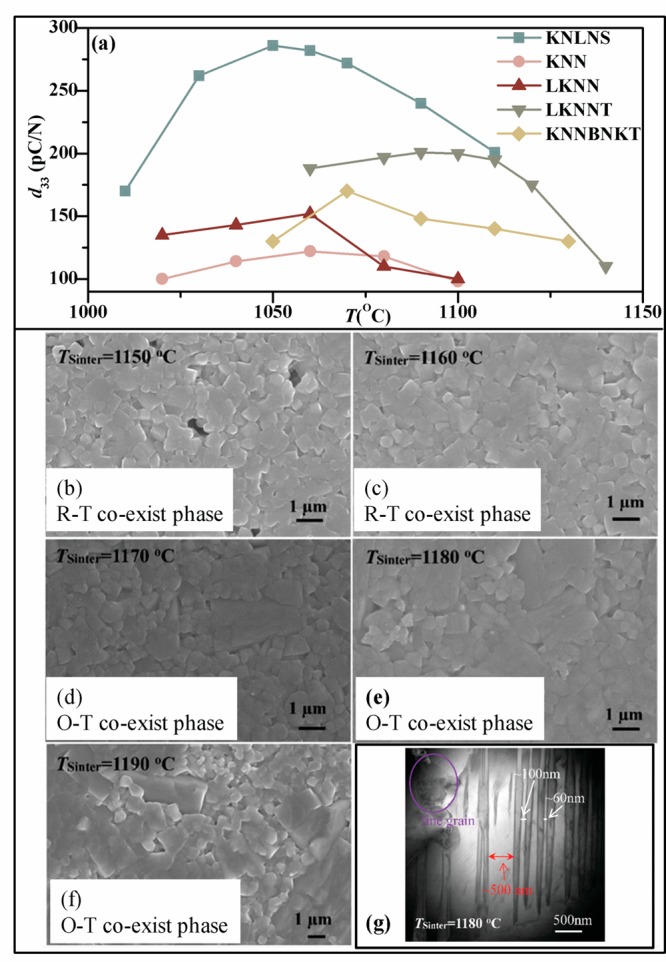
Piezoelectric constant of KNLNS,25 KNN,22 LKNN,22 LKNNT,22 and KNN-BNKT26 ceramics as a function of sintering temperature; scanning electron microscopy images of 0.985(0.96KNNT-0.04BNKZ)-0.015CZ ceramics sintered at (b) 1150 °C, (c) 1160 °C, (d) 1170 °C, (e) 1180 and (f) 1190 °C.24 (g) Transmission electron microscopy image of the ceramic sintered at 1180 °C.24 Reprinted with permission from ref (25). Copyright 2011 Elsevier. Reprinted with permission from ref (22). Copyright 2008 Elsevier. Reprinted with permission from ref (26). Copyright 2014 Taylor & Francis Ltd. Reproduced with permission from ref (24). Copyright 2019 The Royal Society of Chemistry.
2.2.3. Sintering Atmosphere
Sintering atmosphere could affect the existence of oxygen vacancies in KNN-based ceramics and finally influence the microstructure and piezoelectric properties. The influence of synthetic air (80% N2, 20% O2), O2, and Ar sintering atmosphere on the d33 of KNLNTS ceramics was studied, showing that the ceramics sintered in O2 possessed the maximum d33 of 260 pC/N.27 In reducing atmosphere, the valence state of Nb is usually stable and the valence state of Mn ions is +2, which can prevent the decrease of Bi3+, restrain the appearance of a liquid phase, and improve formation of homogeneous grain size, leading to an increase of piezoelectricity. An enhanced d33 of 300 pC/N can be observed in KNN-BNZ-MnO ceramics with R–T sintered in reducing atmosphere (H2/N2/H2O, PO2 = 1 × 10–11 MPa).28
2.3. Poling Condition
The poling process is an important procedure in preparing KNN-based ceramics, in which the domains inside the ceramics would rotate along the outside electric field orientation when the direct current (DC) field or alternating current (AC) field is employed. Generally, the right choice of optimum poling temperature, which is near the polymorphic phase transition temperature, is an efficient way to improve the piezoelectricity regardless of phase structures (see Figure 5a1–d1).29 As shown in Figure 5a2–d2, a saturated d33 of the R–T/O–T/R–O phase structure can be achieved in a low electric field, whereas the d33 of the ceramics with O or T could be saturated under a higher electric field, which was related to domain vibration, domain wall motion, domain switching, electric-field-induced phase transition, and decreased energy barrier initiated from the coexistence of a multiphase structure, revealing that the construction of a multiphase coexistence phase structure was an effective way to achieve high piezoelectricity of KNN-based ceramics under a low electric field.29 In addition, d33 values of KNNS-BHNH ceramics decreased slightly with increased poling temperature in both AC and DC electric fields; furthermore, the d33 increased and remained at a maximum value when the ceramics were poled in both AC and DC electric conditions, whereas a saturated d33 could be easily obtained in DC electric fields compared to the AC electric fields, as shown in Figure 5e1,e2.30
Figure 5.

Piezoelectric constant of (a1) KNNS-0.04BNZ, (b1) KNNS-0.02BNZ, (c1) KNNS, (d1) KNNS-BNZ-CT, and KNN ceramics as a function of poling temperature under the poling electric field of 3 kV/mm.29 (a2–d2) Piezoelectric constant of KNN-based ceramics with different phase structure as a function of poling electric field under optimum poling temperature.29 Piezoelectric constant of KNNS-BHNH ceramics as a function of (e1) poling temperature and (e2) poling electric fields.30 Reprinted from ref (29). Copyright 2016 American Chemical Society. Reproduced with permission from ref (30). Copyright 2017 The Royal Society of Chemistry.
3. Fabrication Technology and Piezoelectricity for Other Types of Materials
In addition to KNN-based ceramics, KNN-based textured ceramics, single crystals, and thin films also have attracted more and more attention. In this part, we mainly introduce the relationship between the preparation method and piezoelectricity of textured ceramics, single crystals, and thin films.
3.1. Textured Ceramics
As shown in Figure 6a, the precursors were prepared by a molten salt synthesis or two-step molten salt method first, and then the obtained precursors were used to form templates using a topochemical microcrystal conversion method. Then, KNN-based powders were fabricated using a conventional solid-state method and then mixed with the prepared templates to form a homogeneous slurry. After that, the mixture was treated by tape casting, followed by a pressing and sintering process, and finally the textured ceramics were synthesized. The procedures for templated grain growth (TGG) and reactive-templated grain growth (RTGG) methods are very similar. The templates in these procedures are plate-like NaNbO3 in the most cases, whereas the templates in the homoepitaxial TGG method and hetero-TGG method are very special. One of the biggest breakthroughs in piezoelectricity of KNN-based ceramics is the discovery of highly ⟨001⟩ textured LF4T ceramics with a d33 of 416 pC/N prepared by the RTGG method.6 Furthermore, ultrahigh d33 of 700 pC/N and an orientation degree of 0.98 were achieved in highly textured KNNS-CZ-BKH ceramics (Figure 6b) prepared by the TGG method using plate-like NaNbO3 as a template, which could be explained by the strong anisotropic feature, optimized domain configuration, facilitated polarization rotation induced by the intermediate M phase, nanodomain structures with decreased domain wall energy, and increased domain wall mobility.3 However, it cannot be ignored that the content of the NN templates must be optimum for each KNN-based ceramic system because the lack or excess templates would accelerate the composition deviation, which could induce the decrease in the piezoelectricity, as shown in Figure 6b.3
Figure 6.

(a) Reaction/homoepitaxial/hetero-templated grain growth process for textured KNN-based ceramics; (b) d33 and orientation degree as a function of NN template content of textured KNNS-CZ-BKH ceramics.3 Reproduced with permission from ref (3). Copyright 2018 John Wiley & Sons Ltd.
3.2. Single Crystals
The piezoelectric property of KNN-based single crystals is higher than those of the polycrystalline counterpart because of the well-aligned polarization orientation and domain engineering in single crystals. KNN-based single crystals have been successfully prepared using various methods, such as flux method, Bridgman method, solid-state crystal growth (SSCG), simple molten salt synthesis (SMSS), seed-free solid-state crystal growth method (SFSSCG), top-seeded solution growth method (TSSG), etc.4 The as-grown single crystals were rectangular or triangular, and those single crystals are not transparent, which may be attributed to the substitution of the doped ions on the A/B sites or the entity of small pores inside the crystals because of the rapid growth of crystals or the presence of many domain walls inside (see Figure 7). In addition, the addition of Mn ions has a big influence on the phase structure and piezoelectric properties of KNN-based single crystals. A high d33 of 545 pC/N with O–T was obtained in KNNLT/Mn single crystals as compared with the d33 of 354 pC/N with pure O in KNNLT single crystals.34 An ultrahigh d33 of 1050 pC/N can be realized in KNN–LiBiO3–MnO2 single crystals with O–T using the SFSSCG method.4
Figure 7.
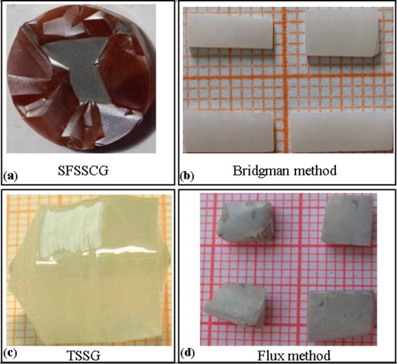
Photographs of as-grown single crystals of (a) K0.5Na0.5NbO3–LiBiO3–MnO2,4 (b) K0.5Na0.5NbO3–LiNbO3,31 (c) (K0.549Na0.451)(Nb0.760Ta0.240)O3,32 and (d) K0.5Na0.5NbO3.33 Reproduced with permission from ref (4). Copyright 2019 The Royal Society of Chemistry. Reprinted with permission from ref (31). Copyright 2007 AIP Publishing. Reproduced with permission from ref (32). Copyright 2013 The Royal Society of Chemistry. Reproduced with permission from ref (33). Copyright 2013 John Wiley & Sons Ltd.
3.3. Thin Films
Large-area deposition films could be obtained utilizing RF magnetron sputtering, but the interface defects induced during high-energy particle bombardment and hardly controlled compositions of films due to the different deposition rates of elements are non-negligible disadvantages. Pulsed laser deposition (PLD) has been widespread used in preparing high-quality films, but the created interface defects during high-energy particle bombardment, the induced composition deviation from the target because of the elements’ different deposition rates, and the lack of large-film preparation are cannot be ignored. The advantages of aerosol deposition are the high deposition rate and the formation of dense films with a thickness of about 1–100 μm at room temperature, but it is hard to obtain the oriented films due to the unordered collisions of particles and substrates. Chemical solution deposition, which is also called the sol–gel method, has attracted much attention due to its homogeneous composition, easy control of chemical composition, the thickness of the obtained films, the ability to prepared large-area films, and the low cost and easy processing procedure. However, it is difficult to produce films thicker than 1 μm, and the films always present a poor piezoelectricity owing to the high leakage current caused by oxygen and alkali ion vacancies. SFSSCG and RTGG, the methods used to prepare single crystals and textured ceramics, can also be utilized to deposit films, which could improve the piezoelectricity by forming an ideal oriented structure and avoiding the influence of substrate clamping.
The electric properties of films are greatly affected by chemical modification, the substrate type and temperature, working temperature and pressure, the distance between the target and the substrate, and the matched degree and residual stress between films and substrates (or electrodes). Shibata et al. prepared KNN films with a high transverse piezoelectric coefficient by annealing optimum temperature after deposition and optimizing the K/Na ratio using the RF method and Pt/Ti/SiO2/Si as the substrate.35 The conductive perovskite oxide electrode, such as LaNiO3, is preferential owing to its close lattice constant with KNN-based films in the RF method.36 PLD epitaxial KNLNT-CZ film exhibited a dielectric constant of 1185 under various oxygen pressures of 15–45 Pa and substrate temperatures of 600–720 °C on a (001)-SrTiO3 substrate utilizing La0.7Sr0.3MnO3 as the bottom electrodes.37 A 28 μm ⟨100⟩-orientated KNLN single-crystal-thick film possessed a superior piezoelectric constant of 490 pm/V prepared using SFSSCG and a new lapping down method.38 In addition, the effect of chemical modification on the electric properties of KNN films has also been reported using the PLD method, such as Ba2+ doping and Sr2+ doping.39
Furthermore, the difficulty of constructing phase boundaries and the existence of composition deviations caused by the volatilization of alkali elements and the lattice mismatch between thin films and substrates (or electrodes) combined lead to the complicated development of high piezoelectric performance thin films. Fortunately, Wang et al. obtained a large orientation degree of 62.8% (see Figure 8a) and effective piezoelectric strain coefficient of 250 pm/V (see Figure 8b) in KNNS-BNKZ0.05 films due to the oriented nanometer scale coexistence of the R–T phase structure with gradual polarization rotation (Figure 8c), which can lower the domain wall energy and improve the piezoelectric property.40 The increased KNNS-BNKZ0.05 thin film thickness of 2.7 μm (see Figure 8d) could produce more free deformation along the thickness direction and promote the domain wall mobility, also leading to the increased piezoelectric property.40
Figure 8.
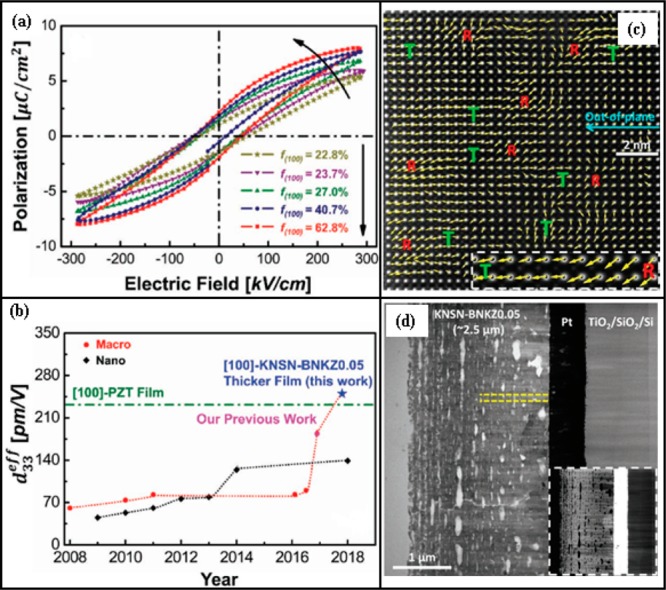
(a) P–E loops with different orientation degree of KNSN-BNKZ0.05 thin films.40 (b) Comparison of the effective piezoelectric strain coefficient of KNN-based thin films and [100]-PZT thin films.40 (c) δNb–Na/K displacement vector maps; the arrows indicate the displacement vectors, and the enlarged image illustrates the gradual polarization rotation from R to T.40 (d) Low-magnification scanning transmission electron microscopy annular bright-field image of KNSN-BNKZ0.05/Pt/TiO2/SiO2/Si; the inset image is a simultaneously obtained scanning transmission electron microscopy high-angle annular dark-field picture.40 Reproduced with permission from ref (40). Copyright 2019 John Wiley & Sons Ltd.
4. Conclusion and Outlook
High piezoelectric constants have been achieved by constructing phase boundaries and choosing optimum sintering processes and poling conditions in KNN-based ceramics. A large piezoelectric coefficient is observed through the construction of the phase structure and employing a suitable prepared method and templates in textured ceramics. The largest piezoelectricity is obtained among the KNN-based lead-free materials by using optimum preparation technology in single crystals. However, the piezoelectricity of KNN-based thin films reported until now is still lower than that of the KNN-based bulk, which needs further investigation. Although it has been statistically shown that prepared methods have played an important part in piezoelectric properties, a comprehensive theoretically model is further needed to find the origin of the high-piezoelectric performance of KNN-based materials. Finally, close attention should be paid to the high performance of KNN-based materials as well as cheaper and more convenient preparation methods. Solving the large-scale preparation issue would be great progress for KNN-based materials. We believe that KNN-based materials would be the most promising alternatives to lead-based materials in commercial applications.
Acknowledgments
Authors gratefully acknowledge the supports of the National Science Foundation of China (NSFC No. 51722208).
Biographies

Nan Zhang is a Ph.D. candidate in the College of Materials Science and Engineering of Sichuan University. Her main research interest is ferroelectric and piezoelectric properties of lead-free KNN-based materials.

Ting Zheng is an associate researcher in the College of Materials Science and Engineering of Sichuan University. Her main research interest is composition design and phase boundary modification of ferroelectric/piezoelectric materials.

Jiagang Wu is a professor and vice dean of the College of Materials Science and Engineering of Sichuan University. His main research interest is the composition design and property modification of ferroelectric/piezoelectric materials.
The authors declare no competing financial interest.
References
- Zheng T.; Wu J.; Xiao D.; Zhu J. Recent development in lead-free perovskite piezoelectric bulk materials. Prog. Mater. Sci. 2018, 98, 552–624. 10.1016/j.pmatsci.2018.06.002. [DOI] [Google Scholar]
- Tao H.; Wu H.; Liu Y.; Zhang Y.; Wu J.; Li F.; Lyu X.; Zhao C.; Xiao D.; Zhu J.; Pennycook S. J. Ultrahigh performance in lead-free piezoceramics utilizing a relaxor slush polar state with multiphase coexistence. J. Am. Chem. Soc. 2019, 141, 13987–13994. 10.1021/jacs.9b07188. [DOI] [PubMed] [Google Scholar]
- Li P.; Zhai J.; Shen B.; Zhang S.; Li X.; Zhu F.; Zhang X. Ultrahigh piezoelectric properties in textured (K,Na)NbO3-based lead-free ceramics. Adv. Mater. 2018, 30, 1705171–1705179. 10.1002/adma.201705171. [DOI] [PubMed] [Google Scholar]
- Jiang M.; Zhang J.; Rao G.; Li D.; Randall C. A.; Li T.; Peng B.; Li L.; Gu Z.; Liu X.; Huang H. Ultrahigh piezoelectric coefficient of a lead-free K0.5Na0.5NbO3-based single crystal fabricated by a simple seed-free solid-state growth method. J. Mater. Chem. C 2019, 7, 14845. 10.1039/C9TC05143K. [DOI] [Google Scholar]
- Dolhen M.; Mahajan A.; Pinho R.; Costa M. E.; Trolliard G.; Vilarinho P. M. Sodium potassium niobate (K0.5Na0.5NbO3, KNN) thick films by electrophoretic deposition. RSC Adv. 2015, 5, 4698–4706. 10.1039/C4RA11058G. [DOI] [Google Scholar]
- Saito Y.; Takao H.; Tani T.; Nonoyama T.; Takatori K.; Homma T.; Nagaya T.; Nakamura M. Lead-free piezoceramics. Nature 2004, 432, 84–87. 10.1038/nature03028. [DOI] [PubMed] [Google Scholar]
- Zheng T.; Wu J. Enhanced piezoelectricity over a wide sintering temperature (400–1050 °C) range in potassium sodium niobate-based ceramics by two step sintering. J. Mater. Chem. A 2015, 3, 6772–6780. 10.1039/C5TA00732A. [DOI] [Google Scholar]
- Yao W.; Zhang J.; Wang X.; Zhou C.; Sun X.; Zhan J. High piezoelectric performance and domain configurations of (K0.45Na0.55)0.98Li0.02Nb0.76Ta0.18Sb0.06O3 lead-free ceramics prepared by two-step sintering. J. Eur. Ceram. Soc. 2019, 39, 287–294. 10.1016/j.jeurceramsoc.2018.09.017. [DOI] [Google Scholar]
- Zhang J.; Qin Y.; Gao Y.; Yao W.; Zhao M. Improvement of physical properties for KNN-based ceramics by modified two-step sintering. J. Am. Ceram. Soc. 2014, 97, 759–764. 10.1111/jace.12794. [DOI] [Google Scholar]
- Zhang Y.; Shen B.; Zhai J.; Zeng H. New insight on sintering progress of KNN-based lead-free ceramics. J. Am. Ceram. Soc. 2016, 99, 752–755. 10.1111/jace.14072. [DOI] [Google Scholar]
- Zhang B. P.; Li J. F.; Wang K.; Zhang H. Compositional dependence of piezoelectric properties in NaxK1-xNbO3 lead-free ceramics prepared by spark plasma sintering. J. Am. Ceram. Soc. 2006, 89, 1605–1609. 10.1111/j.1551-2916.2006.00960.x. [DOI] [Google Scholar]
- Zhen Y.; Li J.-F.; Wang K.; Yan Y.; Yu L. Spark plasma sintering of Li/Ta-modified (K,Na)NbO3 lead-free piezoelectric ceramics: Post-annealing temperature effect on phase structure, electrical properties and grain growth behavior. Mater. Sci. Eng., B 2011, 176, 1110–1114. 10.1016/j.mseb.2011.05.051. [DOI] [Google Scholar]
- Su Y.; Chen X.; Yu Z.; Lian H.; Zheng D.; Peng J. Comparative study on microstructure and electrical properties of (K0.5Na0.5)NbO3 lead-free ceramics prepared via two different sintering methods. J. Mater. Sci. 2017, 52, 2934–2943. 10.1007/s10853-016-0587-z. [DOI] [Google Scholar]
- Yu Z.; Chen X.; Su Y.; Lian H.; Lu J.; Zhou J.; Liu P. Hot-press sintering K0.5Na0.5NbO3-0.5 mol%Al2O3 ceramics with enhanced ferroelectric and piezoelectric properties. J. Mater. Sci. 2019, 54, 13457–13466. 10.1007/s10853-019-03850-9. [DOI] [Google Scholar]
- Yang W.; Li P.; Wu S.; Li F.; Shen B.; Zhai J. A study on the relationship between grain size and electrical properties in (K,Na)NbO3-based lead-free piezoelectric ceramics. Adv. Electron. Mater. 2019, 5, 1900570–1900579. 10.1002/aelm.201900570. [DOI] [Google Scholar]
- Yao F. Z.; Zhang M. H.; Wang K.; Zhou J. J.; Chen F.; Xu B.; Li F.; Shen Y.; Zhang Q. H.; Gu L.; Zhang X. W.; Li J. F. Refreshing piezoelectrics: distinctive role of manganese in lead-free perovskites. ACS Appl. Mater. Interfaces 2018, 10, 37298–37306. 10.1021/acsami.8b14958. [DOI] [PubMed] [Google Scholar]
- Lv X.; Li J.; Men T. L.; Wu J.; Zhang X. X.; Wang K.; Li J. F.; Xiao D.; Zhu J. High-performance 0–3 type niobate-based lead-free piezoelectric composite ceramics with ZnO inclusions. ACS Appl. Mater. Interfaces 2018, 10, 30566–30573. 10.1021/acsami.8b10136. [DOI] [PubMed] [Google Scholar]
- Yin Q.; Yuan S.; Dong Q.; Tian C. Effect of CuO and MnO2 doping on electrical properties of 0.92(K0.48Na0.54)NbO3–0.08LiNbO3 under low-temperature sintering. J. Alloys Compd. 2010, 491, 340–343. 10.1016/j.jallcom.2009.10.168. [DOI] [Google Scholar]
- Zhang M. H.; Wang K.; Du Y. J.; Dai G.; Sun W.; Li G.; Hu D.; Thong H. C.; Zhao C.; Xi X. Q.; Yue Z. X.; Li J. F. High and temperature-insensitive piezoelectric strain in alkali niobate lead-free perovskite. J. Am. Chem. Soc. 2017, 139, 3889–3895. 10.1021/jacs.7b00520. [DOI] [PubMed] [Google Scholar]
- Li L.; Zhen Y. Structure, dielectric and piezoelectric behaviors of (K,Na)NbO3 ceramics with high Qm in low-humidity by introducing SiO2 and CuO mixed oxides. J. Mater. Sci.: Mater. Electron. 2016, 27, 10888–10893. 10.1007/s10854-016-5198-6. [DOI] [Google Scholar]
- Du H.; Liu D.; Tang F.; Zhu D.; Zhou W.; Qu S. Microstructure, piezoelectric, and ferroelectric properties of Bi2O3-added (K0.5Na0.5)NbO3 lead-free ceramics. J. Am. Ceram. Soc. 2007, 90, 2824–2829. 10.1111/j.1551-2916.2007.01846.x. [DOI] [Google Scholar]
- Li J. F.; Zhen Y.; Zhang B. P.; Zhang L. M.; Wang K. Normal sintering of (K, Na)NbO3-based lead-free piezoelectric ceramics. Ceram. Int. 2008, 34, 783–786. 10.1016/j.ceramint.2007.09.025. [DOI] [Google Scholar]
- Ahn C. W.; Park C. S.; Choi C. H.; Nahm S.; Yoo M. J.; Lee H. G.; Priya S. Sintering behavior of lead-free (K,Na)NbO3-based piezoelectric ceramics. J. Am. Ceram. Soc. 2009, 92, 2033–2038. 10.1111/j.1551-2916.2009.03167.x. [DOI] [Google Scholar]
- Cen Z.; Yu Y.; Zhao P.; Chen L.; Zhu C.; Li L.; Wang X. Grain configuration effect on the phase transition, piezoelectric strain and temperature stability of KNN-based ceramics. J. Mater. Chem. C 2019, 7, 1379–1387. 10.1039/C8TC05253K. [DOI] [Google Scholar]
- Liang W.; Xiao D.; Wu W.; Li X.; Sun Y.; Zhu J. Effect of sintering temperature on phase transitions, properties and temperature stability of (K0.465Na0.465Li0.07)(Nb0.95Sb0.05)O3 lead-free piezoelectric ceramics. Curr. Appl. Phys. 2011, 11, S138–S142. 10.1016/j.cap.2011.03.040. [DOI] [Google Scholar]
- Huang T.; Xiao D. Q.; Liang W. F.; Wu J. G.; Wang Z.; Zhu J. G. Sintering behavior of KNN-BNKT lead-free piezoelectric ceramics. Ferroelectrics 2014, 458, 37–42. 10.1080/00150193.2013.849978. [DOI] [Google Scholar]
- Vendrell X.; García J. E.; Rubio-Marcos F.; Ochoa D. A.; Mestres L.; Fernández J. F. Exploring different sintering atmospheres to reduce nonlinear response of modified KNN piezoceramics. J. Eur. Ceram. Soc. 2013, 33, 825–831. 10.1016/j.jeurceramsoc.2012.09.025. [DOI] [Google Scholar]
- Cen Z.; Wang X.; Huan Y.; Li L. Temperature stability and electrical properties of MnO-doped KNN-based ceramics sintered in reducing atmosphere. J. Am. Ceram. Soc. 2018, 101, 2391–2407. 10.1111/jace.15411. [DOI] [Google Scholar]
- Zheng T.; Wu J. Relationship between poling characteristics and phase boundaries of potassium-sodium niobate ceramics. ACS Appl. Mater. Interfaces 2016, 8, 9242–9246. 10.1021/acsami.6b01796. [DOI] [PubMed] [Google Scholar]
- Tao H.; Wu J. New poling method for piezoelectric ceramics. J. Mater. Chem. C 2017, 5, 1601–1606. 10.1039/C6TC05328A. [DOI] [Google Scholar]
- Chen K.; Xu G.; Yang D.; Wang X.; Li J. Dielectric and piezoelectric properties of lead-free 0.95(K0.5Na0.5)NbO3-0.05LiNbO3 crystals grown by the Bridgman method. J. Appl. Phys. 2007, 101, 0441031–0441034. 10.1063/1.2562464. [DOI] [Google Scholar]
- Zheng L.; Huo X.; Wang R.; Wang J.; Jiang W.; Cao W. Large size lead-free (Na,K)(Nb,Ta)O3 piezoelectric single crystal: growth and full tensor properties. CrystEngComm 2013, 15, 7718–7722. 10.1039/c3ce40658j. [DOI] [Google Scholar]
- Saravanan R.; Rajesh D.; Rajasekaran S. V.; Perumal R.; Chitra M.; Jayavel R. Crystal structure, dielectric properties of (K0.5Na0.5)NbO3 single crystal grown by flux method using B2O3 flux. Cryst. Res. Technol. 2013, 48, 22–28. 10.1002/crat.201200282. [DOI] [Google Scholar]
- Huo X.; Zhang R.; Zheng L.; Zhang S.; Wang R.; Wang J.; Sang S.; Yang B.; Cao W. (K, Na, Li)(Nb, Ta)O3:Mn lead-free single crystal with high piezoelectric properties. J. Am. Ceram. Soc. 2015, 98, 1829–1835. 10.1111/jace.13540. [DOI] [PMC free article] [PubMed] [Google Scholar]
- Shibata K.; Suenaga K.; Watanabe K.; Horikiri F.; Nomoto A.; Mishima T. Improvement of piezoelectric properties of (K,Na)NbO3 films deposited by sputtering. Jpn. J. Appl. Phys. 2011, 50, 041503. 10.1143/JJAP.50.041503. [DOI] [Google Scholar]
- Li T.; Wang G.; Li K.; Sama N.; Remiens D.; Dong X. Influence of LNO top electrodes on electrical properties of KNN/LNO thin films prepared by RF magnetron sputtering. J. Am. Ceram. Soc. 2013, 96, 787–790. 10.1111/jace.12047. [DOI] [Google Scholar]
- Li Y. H.; Chen F.; Gao G. Y.; Xu H. R.; Wu W. Ferroelectric, dielectric and leakage current properties of epitaxial (K,Na)NbO3-LiTaO3-CaZrO3 thin films. J. Electroceram. 2015, 34, 249–254. 10.1007/s10832-014-9981-6. [DOI] [Google Scholar]
- Zhang T.; Ou-Yang J.; Yang X.; Wei W.; Zhu B. High performance KNN-based single crystal thick film for ultrasound application. Electron. Mater. Lett. 2019, 15, 1–6. 10.1007/s13391-018-0091-5. [DOI] [Google Scholar]
- Han G.; Ryu J.; Ahn C. W.; Yoon W. H.; Choi J. J.; Hahn B. D.; Kim J. W.; Choi J. H.; Park D. S. High piezoelectric properties of KNN-based thick films with abnormal grain growth. J. Am. Ceram. Soc. 2012, 95, 1489–1492. 10.1111/j.1551-2916.2012.05139.x. [DOI] [Google Scholar]
- Wang Y.; Wu H.; Qin X.; Yao K.; Pennycook S. J.; Tay F. E. H. Outstanding piezoelectric performance in lead-free 0.95(K,Na)(Sb,Nb)O3-0.05(Bi,Na,K)ZrO3 thick films with oriented nanophase coexistence. Adv. Electron. Mater. 2019, 5, 1800691. 10.1002/aelm.201800691. [DOI] [Google Scholar]