Abstract
Multilayer structure is one of the research focuses of thermoelectric (TE) material in recent years. In this work, n-type 800 nm Bi2Te3/(Pt, Au) multilayers are designed with p-type Sb2Te3 legs to fabricate ultrathin microelectromechanical systems (MEMS) TE devices. The power factor of the annealed Bi2Te3/Pt multilayer reaches 46.5 μW cm−1 K−2 at 303 K, which corresponds to more than a 350% enhancement when compared to pristine Bi2Te3. The annealed Bi2Te3/Au multilayers have a lower power factor than pristine Bi2Te3. The power of the device with Sb2Te3 and Bi2Te3/Pt multilayers measures 20.9 nW at 463 K and the calculated maximum output power reaches 10.5 nW, which is 39.5% higher than the device based on Sb2Te3 and Bi2Te3, and 96.7% higher than the Sb2Te3 and Bi2Te3/Au multilayers one. This work can provide an opportunity to improve TE properties by using multilayer structures and novel ultrathin MEMS TE devices in a wide variety of applications.
Keywords: MEMS, Multilayers, TE devices, Bi2Te3
Introduction
Fossil fuels shortages and pollution of environment have raised the attention of researches in recent years. The diversification and efficient multi-level utilization of the energy become important technical approaches to solve these energetic and environmental problems. Thermoelectric (TE) devices show an inherent superiority harvesting the energy generated from waste heat and low quality thermal energy and they constitute a promising way to supply power [1–3]. In addition, TE conversion has particular advantages such as small size, good output quality, no running noise, no pollution, and wide operating temperature range [4–6]. Consequently, TE devices are widely used in wearable devices, vehicles, industrial waste-heat recovery systems and solar energy systems to convert waste heat into electrical energy [7–9]. However, the current conversion efficiency of TE devices is much lower than that of other mechanical systems. The high-efficiency and multi-stage utilization of industrial waste heat, environmental energy recovery, and the development of special power supplies are an urgently needed for the development of TE technologies. Improving the conversion efficiency of TE equipment is a significant challenge in this field. Increasing the conversion efficiency of TE devices corresponds to the enhancement of the performance of the TE materials [10, 11]. The properties of such materials can be determined via the dimensionless figure of merit ZT, which is defined as S2·σ·T·κ−1[12], where S, σ, T, and κ correspond to the Seebeck coefficient, the electrical conductivity, the absolute temperature and the thermal conductivity, respectively. Alternatively, the performance can be also evaluated by using the power factor, PF = S2·σ. In order to boost the thermoelectric conversion efficiency, various approaches to enhance the ZT value have been proposed and developed.
In the 1990s, Hicks and Dresselhaus showed that low-dimensional TE materials, such as quantum wires and quantum wells, exhibit a significantly high ZT values [13, 14]. Using low-dimensional nanostructures to selectively alter the properties of TE materials has been proven to be a new technique to enhance their thermoelectric properties by customizing both their electron and phonon transmission and their scattering characteristics [15–17]. Sun et al. improved the thermoelectric properties of n-type Bi2Te2.7Se0.3 thin films via the introduction of Pt nanoinclusions triggered by pulsed laser deposition [18]. Sumithra et al. introduced semimetal nanoinclusions into Bi2Te3 samples and achieved an enhanced ZT [19].
Although scientists have obtained TE materials with high ZT and PF by using low-dimension and nanostructures, only the performance of most of these materials has been tested but they have not been yet used for practical applications. With the development of Microelectromechanical Systems (MEMS), the preparation and the application of various micro-devices have gradually become a reality. It is more convenient to fabricate low-dimensional TE materials to develop MEMS thermoelectric devices. The micro-nano processing significantly improves the amount of TE modules in a single device, increasing its power output. Therefore, miniaturization is a useful way to enhance the performance of TE devices and to achieve superior quality of integration. Jeffrey et al. fabricated a thermoelectric microdevice containing 126 TE modules via a MEMS-like electrochemical process [20]. A TE device consisting of more than 46,000 (Bi, Sb)2Te3 TE modules electronically connected in series was developed [21]. Highly integrated, ultra thin thermoelectric devices can generate electricity upon a minimal temperature difference, and can convert low-quality thermal energy into electricity.
In this paper, 800 nm n-type Bi2Te3, Bi2Te3/Pt, Bi2Te3/Au multilayers and p-type Sb2Te3 films were prepared and their corresponding TE properties were evaluated. Moreover, three ultrathin TE devices were fabricated by combining different types of the films. To the authors’ knowledge, this is the first time that < 1 μm-TE modules have been build. TE conversion properties of the Sb2Te3, Bi2Te3 and Bi2Te3/(Au, Pt) multilayer thin films were evaluated. In addition, the TE conversion properties were investigated via experiments and theoretical analyses.
Experiments and methods
Fabrication of the TE thin films and MEMS thermoelectric devices
The TE thin films were prepared by alternate sputtering in a high-vacuum magnetron sputtering system at room temperature. The TE multilayers are composed of alternating layers of Bi2Te3 and metal (Pt, Au) with a thickness of 20 and 5 nm with 40 periods, respectively. The sputtering mode used was the radio frequency (RF) method for Sb2Te3 and Bi2Te3 and direct current (DC) technique for Pt and Au. To ensure deposition uniformity, the substrate was rotated at a speed of 20 rpm.
The MEMS thermoelectric devices were fabricated on a monocrystalline silicon wafer covered by a SiO2 layer via a lithography process. Sb2Te3 as the p-type TE modules and Bi2Te3, Bi2Te3/Pt, and Bi2Te3/Au as the n-type TE modules were selected to fabricate the samples. A sheet of 20 nm Cr was deposited as a bonding layer during the fabrication process. Copper was selected as the electrode material due to its thermal conductivity, outstanding electro-conductivity, and its wide use in the currently developed TE devices. Five photomasks containing a graphical architecture were used to prepare the MEMS devices with 572 TE modules in series. Additional file 1: Fig. S1 shows schematically the basic steps of the fabrication process of the MEMS devices. The details of the fabrication method are initially proposed and then, demonstrated as a hybrid fabrication technique for ultrathin thermoelectric devices in a previous work of this research group [22]. In order to prevent the oxidation of copper in the electrode, the sacrificial photoresist was not removed in these MEMS devices. Moreover, this material serves as a supporting structure to ensure that the top electrodes are well interconnected.
Characterizations
The Seebeck coefficient of the Sb2Te3, Bi2Te3 and Bi2Te3/(Au, Pt) multilayers was characterized by using a home-built system. The details of this apparatus are described in a previous study [23]. Furthermore, an oven was used to provide the test ambient temperature. A temperature difference (ΔT) was applied to the both ends of TE films via two Peltier plates, which were controlled by using an adjustable regulated DC power supply. The value of ΔT was varied in the 1–4 K range. The voltage difference (ΔV) was measured by using a data acquisition setup. The Seebeck coefficient was obtained by using the relation S = ΔV·ΔT−1. The representative ΔV − ΔT curves, which were used for the extraction of the Seebeck coefficient are shown in Additional file 1: Fig. S2. The surface morphology and the cross-section microstructures of the fabricated MEMS devices and multilayer thin films were characterized via field emission scanning electron microscopy (SEM). Moreover, both the unannealed and annealed thermoelectric Bi2Te3 and Bi2Te3/(Au, Pt) multilayer thin films were analyzed via Poly-functional X-Ray Diffractometry (XRD) and by using the Hall Effect Measurement System (model: MMR). The thermal conductivity of the annealed TE thin films was obtained via the time-domain thermoreflectance (TDTR) method [24]. The electric power generated by the MEMS devices was measured using a heater and a data acquisition system. The schematic diagram of such devices is shown in Additional file 1: Fig. S3. In order to avoid the oxidation of the copper electrodes, TE devices were only heated up to 463 K.
Results and discussion
Characterizations of the TE thin films
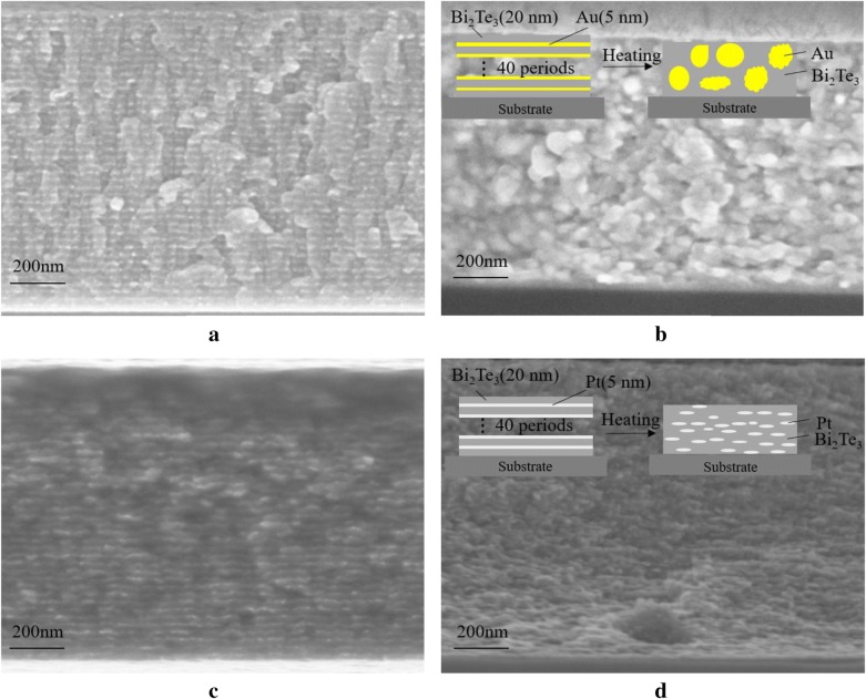
The SEM images of the cross-section of the multilayer thin films before and after the annealing process are shown in Fig. 1. The films were annealed at 473 K for 2 h to simulate the TE modules in the MEMS devices and their photoresist pre-bake process and hard baking, which are involved in their preparation. Figure 1a and c show a fuzzy delamination of both the metal and Bi2Te3 compounds in non-annealed multilayers, respectively. However, the multilayer structure disappears upon annealing and this inevitably influences the properties of the materials. It can be seen from the insets in Fig. 1b and d that Au agglomerates to form large particles after annealing, whereas Pt tends to be uniformly distributed in the Bi2Te3. Moreover, intermittent lamellar structures are still present inside the Bi2Te3/Pt multilayers. This phenomenon can be attributed to the different thermal expansion coefficients of Au and Pt.
Fig. 1.
Cross-section SEM images of the multilayer thin films a Bi2Te3/Au, b annealed Bi2Te3/Au, c Bi2Te3/Pt, d Annealed Bi2Te3/Pt. The insets in b and d show the schematic transformation of the Bi2Te3/Au and Bi2Te3/Pt multilayers as a function of the temperature, respectively
The effects of the pressure on the material can be neglected in a solid, and the volumetric thermal expansion coefficient (αv) can be written as follows:
| 1 |
where v is the volume of the material, Δv corresponds to the volume difference, and ΔT is the temperature difference. At 293 K, the volumetric coefficients of Au and Pt measure 2.7 × 10⁻⁵ K−1 and 4.2 × 10⁻⁵ K−1 respectively [25]. The initial volume of the two multilayer structures is identical, then the volume of the Bi2Te3/Au multilayers becomes about 1.6 times larger than that of the Bi2Te3/Pt multilayers during annealing. This leads to the destruction of the multilayer structure in the Bi2Te3/Au samples. Moreover, Au agglomerates more easily when the multilayer structure is broken. For this reason, many large particles appear in the annealed Bi2Te3/Au multilayers, resulting in a decrease of the compound performance.
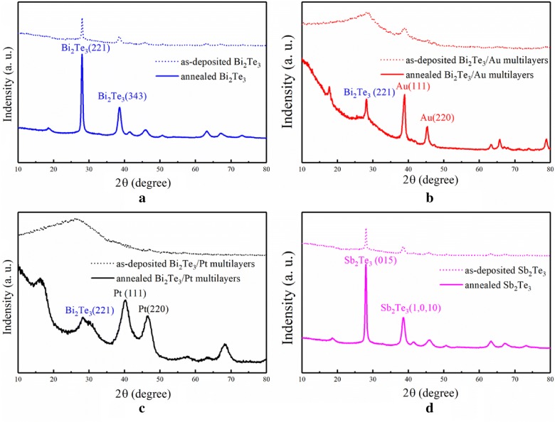
The XRD patterns of the as-deposited and annealed films are presented in Fig. 2. No characteristic peaks derived from additional materials can be observed. Only the Au, Pt, and Bi2Te3 features can be detected in the XRD patterns of the annealed multilayers, indicating that the materials form interstitial solid solutions rather than compounds during the annealing process. In the XRD patterns of the non-annealed multilayers, the characteristic peak of Bi2Te3 with low crystallinity is present, whereas the other two multilayers are amorphous. After annealing under the identical conditions, the pure Bi2Te3 compound exhibits a higher crystallinity than the multilayers material. This implies that the compound was difficult to crystallize due to the presence of the metal particles.
Fig. 2.
XRD patterns of the films, a Bi2Te3/Au, b Bi2Te3/Au, c Bi2Te3/Pt, d Sb2Te3
Estimating the average crystallite size by using the Debye–Scherrer formula [26]:
| 2 |
where D is the average grain size, K is a dimensionless factor with a value of 0.89, λ is the X-ray wavelength, B corresponds to the line broadening at half of the maximum intensity, and θ is the Bragg angle. An average grain size of 9.1 nm, 16.2 nm, and 4.0 nm was obtained for the Bi2Te3, Bi2Te3/Au, and Bi2Te3/Pt multilayers materials, respectively. These results are in agreement with the SEM images.
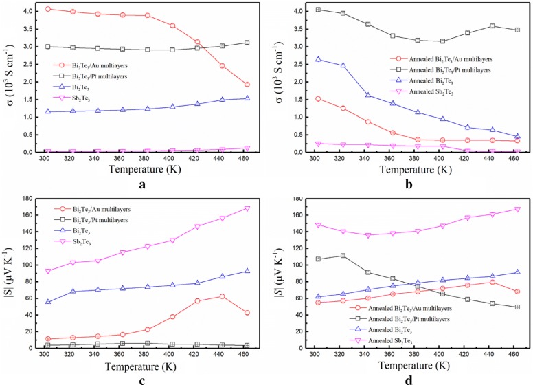
Figure 3 shows the in-plane electrical conductivities and the absolute Seebeck coefficients of the annealed TE film samples in the 303–463 K range. This information helps in understanding their changes upon an increase in the temperature of the multilayer structures. The Sb2Te3 and Bi2Te3 samples exhibit normal semiconductor properties, i.e., their conductivity and Seebeck coefficients increase upon an increase in temperature. A metallic-like behaviour is observed in the Bi2Te3/Au multilayers when Au is introduced. The annealed films show an enhanced conductivity and Seebeck coefficient at 303 K when compared to the non-annealed films. The electrical conductivities of annealed TE films decreases with an increase in temperature while that of Bi2Te3/Pt multilayers rebounds at 423–443 K, this is because the change of crystalline state is a non-monotony variation.
Fig. 3.
Temperature dependence of the in-plane a electrical conductivity, σ, of the deposited films; bσ of the annealed films; c absolute Seebeck coefficient, |S|, of the deposited films; d |S| of the annealed films
The carrier mobility and the concentration of the annealed multilayer films (Table. 1) were compared. The results show numerous electrons accumulate in Au close to its energy barrier. This provides the flow of n-type carrier towards the conduction band of Bi2Te3 when Au starts agglomerating. Moreover, the directional movement of the electrons is limited, leading to a reduction in the electrical conductivity of the Bi2Te3/Au multilayers upon an increase in temperature. However, due to the higher thermal stability of platinum, the multilayer structure remains almost unchanged in the Bi2Te3/Pt multilayer film when the temperature is changed. Thus, the Bi2Te3/Pt multilayers exhibit a stable electrical conductivity temperature profile. The increase in the electrical conductivity of the Bi2Te3/Pt multilayers is mostly correlated to an increase in mobility.
Table 1.
Carrier concentration, mobility and TE properties of the annealed films at 303 K
| Types of films | Sb2Te3 | Bi2Te3 | Bi2Te3/Au multilayer | Bi2Te3/Pt multilayer |
|---|---|---|---|---|
| Type of carrier | Holes | Electrons | Electrons | Electrons |
|
Carrier concentration [cm−3] |
(2.9 ± 0.3) × 1020 | (1.8 ± 0.2) × 1021 | (6.8 ± 0.1) × 1021 | (2.0 ± 0.2) × 1021 |
|
Carrier mobility [cm2 V−1 s−1] |
5.7 ± 0.2 | 8.77 ± 0.4 | 1.5 ± 0.1 | 13.2 ± 0.2 |
|
Seebeck coefficient [μV K−1] |
148.4 ± 1.0 | 62.0 ± 0.3 | 55.0 ± 1.1 | 107.05 ± 1.1 |
|
Electrical conductivity [S cm−1] |
252 ± 6 | 2638 ± 58 | 1525 ± 81 | 4054 ± 11 |
|
Power factor [μW cm−1 K−2] |
5.5 ± 0.6 | 10.1 ± 0.4 | 4.61 ± 0.7 | 46.5 ± 0.5 |
In the deposited multilayers, if the metal layer is not broken, the metal layer generates a short cut in the test circuit, leading to a low Seebeck coefficient, as shown in Fig. 3c. The increase of the Seebeck coefficient in the annealed multilayers is generated by the heat of the metal layer, when it is embedded into the semiconductor matrix as a secondary non-inclusion phase. The energy-dependent carrier scattering effect is introduced into the bending band of Fermi level alignment at the metal/semiconductor interface, to scatter low-energy carriers and improve |S|, but hardly significantly reducing conductivity [27, 28].
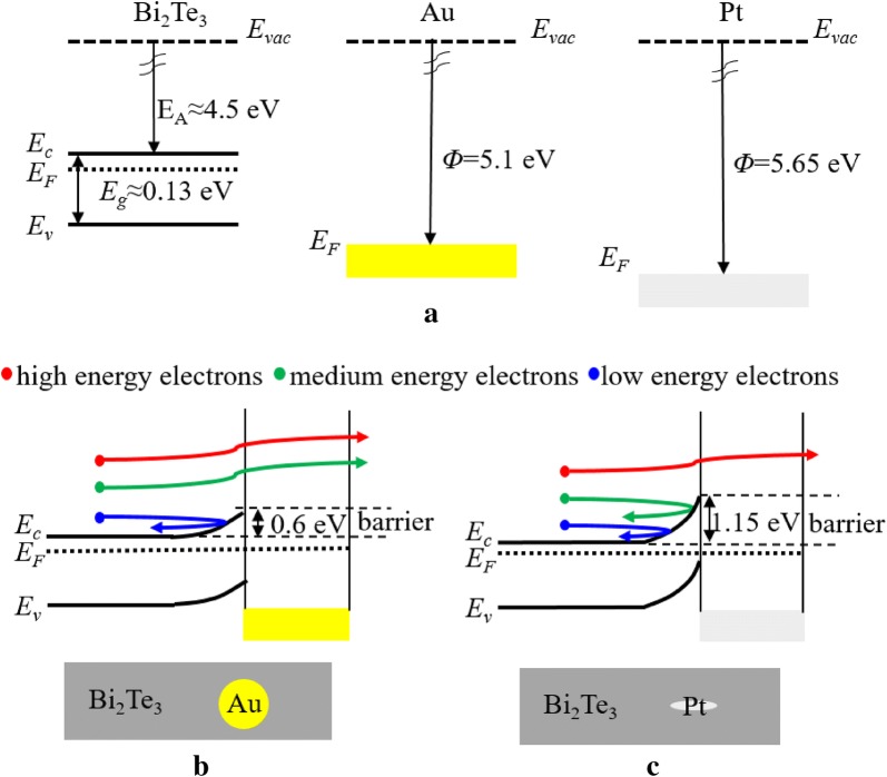
The band alignments of Bi2Te3, Au and Pt are shown in Fig. 4a. The band gap (Eg), the electron affinity (EA) of Bi2Te3, and the work function (Φ) of Au and Pt are estimated from their bulk values [19, 29]. The equilibrium band diagrams of Au-Bi2Te3 and Pt-Bi2Te3 at the metal–semiconductor interface are illustrated in Fig. 4b and c, respectively. The results indicate the formation of a band bending potential barrier at the interface. Moreover, no interface defect states (causing the Fermi level pinning) are observed.
Fig. 4.
a Band energy diagram of Bi2Te3, Pt, and Au before contact. The band gap, electron affinity, and ionization potential of Bi2Te3 and the work function of Pt and Au are estimated from their bulk values; b Equilibrium band alignment of Bi2Te3 and Pt after contact; c Equilibrium band alignment of Bi2Te3 and Au after contact. No interface defect states are taken into account
As described above, the barrier created by the bending of the Pt/Bi2Te3 and Au/Bi2Te3 interfaces promotes a “selective” block of the low energy electrons, causing an increase in the average carrier energy, which leads to an increase of |S|. Usually, there is a Schottky barrier at the metal–semiconductor interface, which depands mostly on the difference between the EA of the semiconductor and the work function of the metal. Pt shows to have an advantage due to its higher work function when compared to Au. This generates the formation of a higher Schottky barrier when Pt is combined with the Bi2Te3 n-type semiconductor (with EA of 4.5 eV). In this case, the average carrier energy in Bi2Te3/Pt multilayers is higher and thus, a higher |S| is obtained. Moreover, the enhancement of the |S| can be expressed via the Mott relation:
| 3 |
where kB is the Boltzmann constant, T is the absolute temperature, q is the electronic charge, σ(E) is the electrical conductivity, corresponds to the carrier concentration, and μ(E) to the carrier mobility, which depends on the energy. In the Bi2Te3/Au multilayers, the huge increase in the carrier concentration causes a negative influence, which results in a lower |S| value when compared to Bi2Te3.
The cross-plane thermal conductivity of the annealed Bi2Te3 is 1.33 W m−1 K−1, whereas that of the annealed Bi2Te3/Au and Bi2Te3/Pt multilayers is 1.39 and 1.22 W m−1 K−1, respectively. This shows that the disappearance of the multilayer structure in the Bi2Te3/Au multilayers leads to an increase in their thermal conductivity: the residual multilayer structure of the samples effectively scatters the phonons and reduces the thermal conductivity of the material. The cross-plane thermal conductivity of the annealed Sb2Te3 sample measures 1.06 W m−1 K−1.
Characterizations of the TE devices
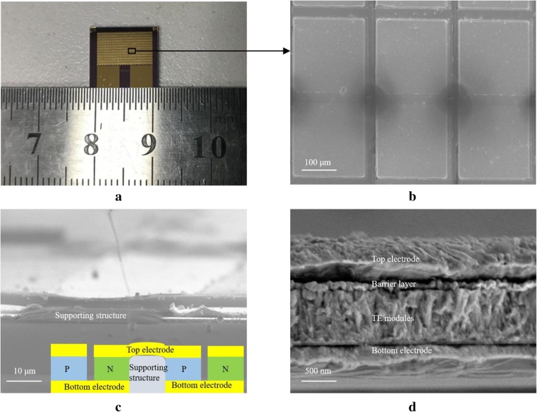
To investigate the power-generation capability of the Bi2Te3/(Au, Pt) multilayers, three types of MEMS thermoelectric devices with the same p-type TE module consisting of Sb2Te3 and different n-type TE modules were designed and prepared. As an example, here the results of the MEMS devices fabricated with a n-type TE module consisting of pristine Bi2Te3, Bi2Te3/Au multilayers, or Bi2Te3/Pt multilayers (labelled ST-BT, ST-BA, or ST-BP, respectively) are reported. One of the individual devices, consisting of 572 thermoelectric modules, is shown in Fig. 5a. Its SEM images are illustrated in Fig. 5b–d. Figure 5b, c prove that the electric-connected top electrode has been deposited smoothly. Each TE module has a size of 200 × 200 × 0.8 μm, and the dark area in Fig. 5b illustrates the organic support structure. The height of the supporting structure in Fig. 5c is relatively consistent with the thermoelectric column, which ensures the smooth conduction of the top electrode. The inset in Fig. 5c shows the schematic diagram of the TE devices. The barrier layer in Fig. 5d is a layer of gold with a thickness of 100 nm, which exists above the thermoelectric material to prevent the surface of the thermoelectric material from being oxidized or corroded. The small gap between the top electrode and the thermoelectric modules, which one can observe in Fig. 5d, is caused by the stress generated during the sample preparation. The SEM image of the cross plane of a single thermoelectric leg also illustrates that the Bi2Te3/metal multilayer structure in the MEMS devices disappears and is replaced by a hybrid structure. Hard baking is necessary to build a supporting structure and this results in the diffusion of the metal and Bi2Te3. This process corresponds to the disappearance of multilayers structure and introduction of metal nano-inclusions. The diffusion in the multilayer structure while heating constitutes a problem, which has to be solved in practical applications of such multilayers. The rough interfaces between the electrode and the TE modules generate a considerable contact thermal resistance, which significantly decreases the temperature difference of the TE module. Thus, by optimizing the structure of devices and TE modules, the performance of TE devices can be significantly enhanced.
Fig. 5.
a Photograph of an actual fabricated MEMS device; b SEM image of the local structure in the MEMS device; c SEM cross-sectional view of the cross-plane of the supporting structure; d SEM cross-sectional view of the cross plane of a single thermoelectric leg. The inset shown in c shows the schematic diagram of the TE devices
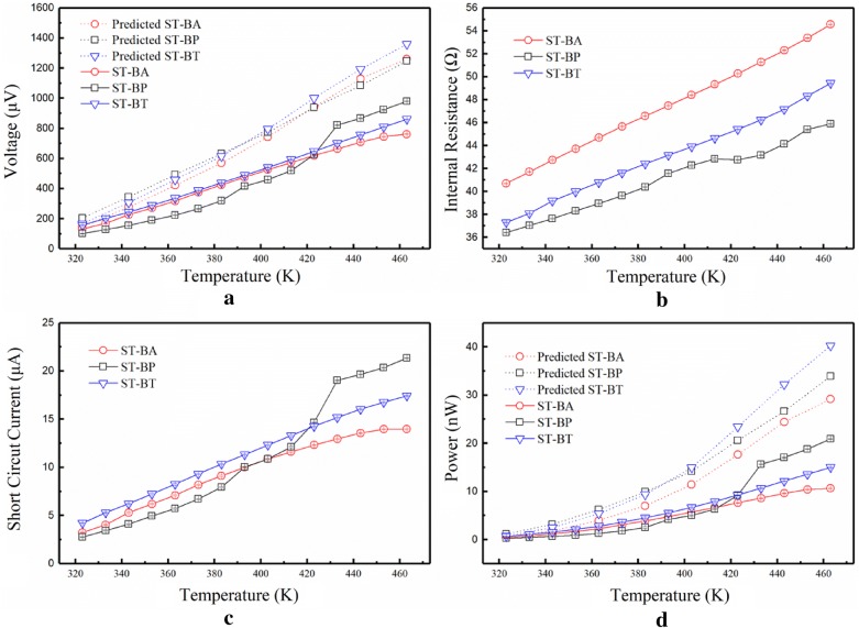
The output characteristics and the internal resistance as a function of the temperature are shown in Fig. 6. From the growth trend of the curve reported in Fig. 6d, it can be deduced that the performance growth of ST-BA tends to stagnate. This may be due to the decrease of the in-plane Seebeck coefficient of the annealed Bi2Te3/Au multilayers at 463 K and to the isotropic morphology of the annealed Bi2Te3/Au multilayers. Initially, the performance of ST-BP is lower than that of the other two compounds, but between 413 and 433 K its internal resistance hardly changes during and its short circuit voltage rises sharply. Despite, the experimental limitation in the measurement of the cross-plane |S| of thin films, one can speculate that the cross-plane |S| of the Bi2Te3/Pt multilayers increases between 413 and 443 K, due to a Schottky barrier. The power of ST-BP reaches 20.9 nW at 463 K, which corresponds to an enhancement larger than 39.5% when compared to ST-BT. One can conclude that when the external load is equivalent to its internal resistance, the calculated maximum output power of ST-BP reaches 10.5 nW at 463 K, and the output power density is 0.02 W m−2 and 2.88 × 10⁴ W m−3. In addition, if a forced cold end is added to the existent cold end of the device, the output can be increased by one to two orders of magnitude [22]. The in-plane Seebeck coefficient of the Bi2Te3/Au multilayers decreases upon an increase of the temperature, leading to the superior properties of the ST-BP material at high temperature. Moreover, these results show that the annealed Bi2Te3/Pt multilayers are anisotropic.
Fig. 6.
Electrical properties of the TE device measured at various temperatures; a Voltage; b Resistance; c Short circuit current; d Output power. The dotted lines in a and d show the analytical model results
The TE devices were analyzed by using the method proposed in the Refs [30, 31]. The one-dimensional heat transfer equation applies to all the TE devices and relates the voltage and the temperature difference and the power output to the load. The power output and the voltage of the TE devices can be calculated as follows:
| 4 |
| 5 |
where TCs and THs corresponds to the temperatures at the cold and hot surfaces, respectively, I is the electrical load current, and r is the internal electrical resistance. The heat transfer mechanism is based on the Seebeck effect, on the conduction effect, and on the Joule effect in p-type and n-type semiconductor blocks. For this reason, the rate of the heat entering from the hot side of the device, QH, and the rate of the heat leaving from its cold side, QC, can be expressed as:
| 6 |
| 7 |
where S is the Seebeck coefficient of the TE legs, THs and TCs correspond to the hot and cold surface temperature, and κ is the thermal conductivity. If the temperature is inconstant, the energy balance equations between the hot and the cold side of the TE device can be expressed as:
| 8 |
| 9 |
where h1 and h2 correspond to the equivalent convection heat transfer coefficients of the hot and cold side, and A1 and A2 are the hot and cold heat transfer surface area of the devices, respectively. By solving Eqs. (6) and (7), THs and TCs are expressed as:
| 10 |
| 11 |
The values of Seebeck coefficients and the thermal conductivities of the TE legs were taken from results obtained from the annealed films measured above. The heat transfer coefficient for the heat transfer model considered is 12.16 W m−2 K−1 and it is based on Ref. [32]. The hot heat transfer surface area measures 1.44 mm2 and the cold heat transfer surface area considered is 0.46 mm2. Figure 6a and d show the predicted results of the TE devices found on Eqs. (4)–(11). In Fig. 6a, the open circuit voltage of the ultrathin TE devices increases upon an increase in the temperature difference. The difference between the simulated and experimental results for ST-BP reflects the cross-plane TE properties of TE modules, whereas the in-plane TE properties were used for analysis. The simulation results of ST-BA and ST-BT are in agreement with the measured values, indicating that the annealed Bi2Te3 and Bi2Te3/Au multilayers are isotropic. Although a more accurate simulation cannot be obtained due to the experimental limitations in the measurement of the cross-plane |S| of the thin film samples, these devices could be a way to evaluate the cross-plane Seebeck coefficient of thin film materials.
Conclusions
In conclusion, 800-nm-thick n-type Bi2Te3, Bi2Te3/Au, Bi2Te3/Pt multilayers and p-type Sb2Te3 films were used to fabricate ultra-thin MEMS devices. The thermal stability of the evolution of the nanostructures and their corresponding thermoelectric properties before and after annealing were investigated. The Au compound in the Bi2Te3/Au multilayers agglomerates and limits the directional movement of the electrons, causing a significant drop in the conductivity and in the power factor. While the Bi2Te3/Pt multilayers still maintains a lamellar-like structure due to the excellent thermal stability of Pt, both the Seebeck coefficient and the conductivity increase. Therefore, a high-power factor of 46.5 μW cm−1 K−2 is obtained at 303 K by annealing the Bi2Te3/Pt multilayers to force the Pt layer to embed nano-inclusions into the Bi2Te3 matrix.
In addition, the thermoelectric conversion properties of the Bi2Te3 and Bi2Te3/(Au, Pt) multilayers were evaluated by measuring the properties of the MEMS devices. The output characteristics of the three devices are similar when the temperature is lower than 423 K. The no-load power of ST-BP reaches 20.9 nW, which corresponds to an enhancement larger than 39.5% when compared to ST-BT for a temperature higher than 423 K. This research facilitates the optimization of the microstructures and materials to fabricate thermoelectric modules and contributes to the development of novel applications of the low-dimensional thermoelectric materials in ultra-thin TE devices.
Supplementary information
Additional file 1: Ultrathin MEMS thermoelectric generator with Bi2Te3/(Pt, Au) multilayers and Sb2Te3 legs.Fig. S1.Schematic outlining the basic steps of the fabrication processes for the ultrathin thermoelectric devices. (a) Positive photoresist coating on the substrate baking. (b) UV exposing (need align except for the first time). (c) Developing the exposure areas. (d) Depositing of bottom electrode. (e) Patterning using the lift-off technique. (f) UV exposing and depositing of TE modules. (g) Patterning using the lift-off technique. (h) UV exposing and depositing of another TE modules. (i) Patterning using the lift-off technique. (j) Supporting structure made by the vitrified photoresist. (k) UV exposing and depositing of top electrode. (l) Patterning using the lift-off technique. Fig. S2. Representative ΔV-ΔT curves of Sb2Te3, Bi2Te3 and Bi2Te3/(Au, Pt) multilayers; (a) Bi2Te3 before annealing, (b) Bi2Te3 after annealing, (c) Bi2Te3/Au multilayers before annealing, (d) Bi2Te3/Au multilayers after annealing, (e) Bi2Te3/Pt multilayers before annealing, (f) Bi2Te3/Pt multilayers after annealing, (g) Sb2Te3 before annealing, (h) S2Te3 after annealing. Fig. S3.Schematic diagram of the experimentally tested device.
Acknowledgements
Not applicable
List of symbols
- A1
contact area of the hot side (mm2)
- A2
contact area of the cold side (mm2)
- B
line broadening at half the maximum intensity (rad)
- D
mean size of the ordered domains (nm)
- EA
electron affinity (eV)
- Ec
the energy at the bottom of the conduction band (eV)
- EF
Fermi level (eV)
- Eg
band gap (eV)
- Ev
the energy at the top of the valence band (eV)
- Evac
vacuum level (eV)
- h1
equivalent convection heat transfer coefficient of hot side (W m−2 K−1)
- h2
equivalent convection heat transfer coefficient of cold side (W m−2 K−1)
- I
open circuit output current of the TE device (A)
- kB
Boltzmann constant
- K
Scherrer constant
- n(E)
carrier concentration (cm−3)
- q
quantity of electric charge
- QC
rate of heat entering from the hot side of the TE device (W)
- QH
rate of heat leaving from the cold side of the TE device (W)
- r
internal resistance value of TE device (Ω)
- S
Seebeck coefficient (V K−1)
- T
absolute temperature (K)
- TC
cold side temperature (K)
- TCs
cold surface temperature of TE device (K)
- THs
hot surface temperature of TE device (K)
- U
open circuit output voltage of the TE device (V)
- v
volume of the material (m3)
Greek symbols
- αv
volumetric thermal expansion coefficient
- ΔT
temperature difference (K)
- Δv
volume difference (cm3)
- ΔV
voltage difference (V)
- σ(E)
electrical conductivity (S cm−1)
- κ
thermal conductivity (W m−1 K−1)
- μ(E)
carrier mobility (cm2 V−1 s−1)
- θ
Bragg angle (degree)
- Φ
work function (eV)
Abbreviations
- DC
direct current
- MEMS
microelectromechanical systems
- PF
power factor
- RF
radio frequency
- SEM
scanning electron microscope
- TDTR
time-domain thermoreflectance
- TE
thermoelectric
- XRD
X-ray diffraction
- ZT
thermoelectric figure of merit
Authors' contributions
YL as the first author completed the collation of the article data and the writing of the entire article; EM and ZW provide some data in the article. ZC, FS and XW contributed to the thermal conductivity. XF and FW help to prepare the TE devices. ZH directed entire research at Shanghai Jiao Tong University and contributed to the manuscript preparation. All authors read and approved the final manuscript.
Funding
This research was supported by National Natural Science Foundation of China (Grant No: 51776126 and 51606193), Yunnan Hu Zhiyu Expert Workstation [(2014) 5]. The authors would like to thank the Center for Advanced Electronic Materials and Devices (AEMD) of Shanghai Jiao Tong University and Instrumental Analysis Center, and the startup fund of Shanghai Jiao Tong University.
Availability of data and materials
The datasets used and/or analyzed during the current study are available from the corresponding author on reasonable request.
Competing interests
The authors declare that they have no competing interests.
Footnotes
Publisher's Note
Springer Nature remains neutral with regard to jurisdictional claims in published maps and institutional affiliations.
Contributor Information
Yang Liu, Email: miemiemie@sjtu.edu.cn.
Erzhen Mu, Email: muerzhen@sjtu.edu.cn.
Zhenhua Wu, Email: wuzhenhua@sjtu.edu.cn.
Zhanxun Che, Email: chezhanxun@iet.cn.
Fangyuan Sun, Email: sunfangyuan@iet.cn.
Xuecheng Fu, Email: xuecheng.f@sjtu.edu.cn.
Fengdan Wang, Email: fdwang@sjtu.edu.cn.
Xinwei Wang, Email: wangxw@upc.edu.cn.
Zhiyu Hu, Email: zhiyuhu@sjtu.edu.cn.
Supplementary information
Supplementary information accompanies this paper at 10.1186/s40580-020-0218-x.
References
- 1.Cornett J, Chen B, Haidar S, Berney H, McGuinness P, Lane B, Gao Y, He Y, Sun N, Dunham M, Asheghi M, Goodson K, Yuan Y, Najafi K. J. Electron. Mater. 2017;46(5):2844–2846. doi: 10.1007/s11664-016-4992-5. [DOI] [Google Scholar]
- 2.Yan J, Liao X, Yan D, Chen Y. J. Microelectromech. S. 2018;27(1):1–18. doi: 10.1109/JMEMS.2017.2782748. [DOI] [Google Scholar]
- 3.Ran H, Schierning G, Nielsch K. Adv. Mater. Technol. 2017;3(4):1700256. [Google Scholar]
- 4.Xie J, Lee C, Feng H. J. Microelectromech. S. 2010;19(2):317–324. doi: 10.1109/JMEMS.2010.2041035. [DOI] [Google Scholar]
- 5.Hadjistassou C, Kyriakides E, Georgiou J. Energy. Convers Manage. 2013;66(66):165–172. doi: 10.1016/j.enconman.2012.07.030. [DOI] [Google Scholar]
- 6.Lim JR, Whitacre JF, Fleurial J-P, Huang C-K, Ryan MA, Myung NV. Adv. Mater. 2005;17(12):1488–1492. doi: 10.1002/adma.200401189. [DOI] [Google Scholar]
- 7.Chen B, Kruse M, Xu B, Tutika R, Zheng W, Bartlett MD, Wu Y, Claussen JC. Nanoscale. 2019;11(12):5222–5230. doi: 10.1039/C8NR09101C. [DOI] [PubMed] [Google Scholar]
- 8.Bell LE. Science. 2008;321(5895):1457–1461. doi: 10.1126/science.1158899. [DOI] [PubMed] [Google Scholar]
- 9.Kim SJ, We JH, Cho BJ. Energy Environ. Sci. 2014;7(6):1959–1965. doi: 10.1039/c4ee00242c. [DOI] [Google Scholar]
- 10.Minnich AJ, Dresselhaus MS, Ren ZF, Chen G. Energy Environ. Sci. 2009;2(5):466–479. doi: 10.1039/b822664b. [DOI] [Google Scholar]
- 11.Zebarjadi M, Esfarjani K, Dresselhaus MS, Ren ZF, Chen G. Energy Environ. Sci. 2012;5(1):5147–5162. doi: 10.1039/C1EE02497C. [DOI] [Google Scholar]
- 12.Slack G. CRC handbook of thermoelectrics. Florida: CRC Press; 1995. [Google Scholar]
- 13.Hicks LD, Dresselhaus MS. Phys. Rev. B. 1993;47(19):12727–12731. doi: 10.1103/PhysRevB.47.12727. [DOI] [PubMed] [Google Scholar]
- 14.Hicks LD, Dresselhaus MS. Phys. Rev. B. 1993;47(24):16631–16634. doi: 10.1103/PhysRevB.47.16631. [DOI] [PubMed] [Google Scholar]
- 15.Venkatasubramanian R, Siivola E, Colpitts T, O'Quinn B. Nature. 2001;413(6856):597–602. doi: 10.1038/35098012. [DOI] [PubMed] [Google Scholar]
- 16.Lee H, Anoop G, Lee H, Kim WS, Jo J. RSC Advances. 2019;9:11595–11601. doi: 10.1039/C9RA02112D. [DOI] [PMC free article] [PubMed] [Google Scholar]
- 17.Dresselhaus MS, Chen G, Tang MY, Yang RG, Lee H, Wang DZ, Ren ZF, Fleurial J-P, Gogna P. Adv. Mater. 2007;19(8):1043–1053. doi: 10.1002/adma.200600527. [DOI] [Google Scholar]
- 18.Sun T, Samani MK, Khosravian N, Ang KM, Yan Q, Tay BK, Hng HH. Nano Energy. 2014;8(9):223–230. doi: 10.1016/j.nanoen.2014.06.011. [DOI] [Google Scholar]
- 19.Sumithra S, Takas NJ, Misra DK, Nolting WM, Poudeu PFP, Stokes KL. Adv. Energy Mater. 2011;1(6):1141–1147. doi: 10.1002/aenm.201100338. [DOI] [Google Scholar]
- 20.Jeffrey SG, Lim JR, Huang C-K, Fleurial J-P. Nat. Mater. 2003;2(8):528. doi: 10.1038/nmat943. [DOI] [PubMed] [Google Scholar]
- 21.Mu E, Wu Z, Wu Z, Chen X, Liu Y, Fu X, Hu Z. Nano Energy. 2019;55:494–500. doi: 10.1016/j.nanoen.2018.10.057. [DOI] [Google Scholar]
- 22.Mu E, Yang G, Fu X, Wang F, Hu Z. J. Power Sources. 2018;394:17–25. doi: 10.1016/j.jpowsour.2018.05.031. [DOI] [Google Scholar]
- 23.Wu Z, Mu E, Wang Z, Chen X, Wu Z, Liu Y, Hu Z. Cryst Growth Des. 2019;19(7):3639–3646. doi: 10.1021/acs.cgd.8b01632. [DOI] [Google Scholar]
- 24.Chang G, Sun F, Duan J, Che Z, Wang X, Wang J, Kim MJ, Zhang H. Acta Mater. 2018;160:235–246. doi: 10.1016/j.actamat.2018.09.004. [DOI] [Google Scholar]
- 25.Turcotte DL, Schubert G. Geodynamics. 2. Cambridge: Cambridge University Press; 2002. [Google Scholar]
- 26.Edwards AJ. Anal. Chim. Acta. 1975;77:349. doi: 10.1016/S0003-2670(01)95199-2. [DOI] [Google Scholar]
- 27.Faleev SV, Léonard F. Phys. Rev. B. 2008;77(21):214304. doi: 10.1103/PhysRevB.77.214304. [DOI] [Google Scholar]
- 28.Zebarjadi M, Esfarjani K, Shakouri A, Bahk J-H, Bian Z, Zeng G, Bowers J, Lu H, Zide J, Gossard A. Appl. Phys. Lett. 2009;94(20):202105. doi: 10.1063/1.3132057. [DOI] [Google Scholar]
- 29.Lide DR. CRC Handbook of Chemistry and Physics. Florida: CRC Press; 2008. [Google Scholar]
- 30.Shen Z-G, Wu S-Y, Xiao L, Yin G. Energy. 2016;95:367–379. doi: 10.1016/j.energy.2015.12.005. [DOI] [Google Scholar]
- 31.Chen L, Gong J, Sun F, Wu C. Int. J. Therm. Sci. 2002;41(1):95–99. doi: 10.1016/S1290-0729(01)01307-2. [DOI] [Google Scholar]
- 32.Siddique ARM, Rabari R, Mahmud S, Heyst BV. Energy. 2016;115:1081–1091. doi: 10.1016/j.energy.2016.09.087. [DOI] [Google Scholar]
Associated Data
This section collects any data citations, data availability statements, or supplementary materials included in this article.
Supplementary Materials
Additional file 1: Ultrathin MEMS thermoelectric generator with Bi2Te3/(Pt, Au) multilayers and Sb2Te3 legs.Fig. S1.Schematic outlining the basic steps of the fabrication processes for the ultrathin thermoelectric devices. (a) Positive photoresist coating on the substrate baking. (b) UV exposing (need align except for the first time). (c) Developing the exposure areas. (d) Depositing of bottom electrode. (e) Patterning using the lift-off technique. (f) UV exposing and depositing of TE modules. (g) Patterning using the lift-off technique. (h) UV exposing and depositing of another TE modules. (i) Patterning using the lift-off technique. (j) Supporting structure made by the vitrified photoresist. (k) UV exposing and depositing of top electrode. (l) Patterning using the lift-off technique. Fig. S2. Representative ΔV-ΔT curves of Sb2Te3, Bi2Te3 and Bi2Te3/(Au, Pt) multilayers; (a) Bi2Te3 before annealing, (b) Bi2Te3 after annealing, (c) Bi2Te3/Au multilayers before annealing, (d) Bi2Te3/Au multilayers after annealing, (e) Bi2Te3/Pt multilayers before annealing, (f) Bi2Te3/Pt multilayers after annealing, (g) Sb2Te3 before annealing, (h) S2Te3 after annealing. Fig. S3.Schematic diagram of the experimentally tested device.
Data Availability Statement
The datasets used and/or analyzed during the current study are available from the corresponding author on reasonable request.


