Abstract
This paper presents a novel on-chip antenna using standard CMOS-technology based on metasurface implemented on two-layers polyimide substrates with a thickness of 500 μm. The aluminium ground-plane with thickness of 3 μm is sandwiched between the two-layers. Concentric dielectric-rings are etched in the ground-plane under the radiation patches implemented on the top-layer. The radiation patches comprise concentric metal-rings that are arranged in a 3 × 3 matrix. The antennas are excited by coupling electromagnetic energy through the gaps of the concentric dielectric-rings in the ground-plane using a microstrip feedline created on the bottom polyimide-layer. The open-ended feedline is split in three-branches that are aligned under the radiation elements to couple the maximum energy. In this structure, the concentric metal-rings essentially act as series left-handed capacitances CL that extend the effective aperture area of the antenna without affecting its dimensions, and the concentric dielectric rings etched in the ground-plane act as shunt left-handed inductors LL, which suppress the surface-waves and reduce the substrates losses that leads to improved bandwidth and radiation properties. The overall structure behaves like a metasurface that is shown to exhibit a very large bandwidth of 0.350–0.385 THz with an average radiation gain and efficiency of 8.15dBi and 65.71%, respectively. It has dimensions of 6 × 6 × 1 mm3 that makes it suitable for on-chip implementation.
Subject terms: Electrical and electronic engineering, Electronic devices
Introduction
Antenna is the key component to enable wireless communication however their physical size is a function of the operating frequency. Applications of on-chip antennas is therefore limited to high-frequencies due to the large size of antenna at lower frequencies. Off chip antennas however offer the benefit of radiation efficiency as they can be implemented on low-loss dielectric substrates1–6..
Currently, antennas for front-end transceivers can be realised using three different methods, which include: (i) Antenna-in-Package (AiP), where the antenna is embedded in the IC’s packaging; (ii) Antenna-on-Chip (AoC), where the antenna is realized on substrate; and (iii) this is a hybrid of AoC and AiP, where the radiating element is realized off-chip. Wire bonding and flip chip are the two commonly used interconnections techniques employed in AiP to connect the die and the antenna7. These types of interconnects are highly lossy at high frequencies due to impedance mismatch. The only viable solution to overcome this loss is by using on-chip antenna, which should significantly reduce the manufacturing cost of system-on-chip (SoC).
The development of a truly efficient cost effective on-chip antenna is a challenging endeavour. The main challenges are attributed to (1) low resistivity of dielectric substrates, which is approximately 10 ohm-cm, contributes to substrate loss of 85% whereas metallization loss is only 15%; (2) high permittivity substrate confines most of the electromagnetic energy in the substrate rather than being radiated into free-space, which adversely affect radiation efficiency8; (3) no specific design rule for antenna design in standard technologies for on-chip antennas. Also, the typical metallization thickness using standard technologies results in poor radiation because thin metal layer has a high resistance; and (4) on-chip antenna’s radiation characteristics cannot be measured in an anechoic chamber unless the chip is mounted on a special test fixture. Mounting the chip on a test fixture can results in undesirable radiation because of interference from nearby circuit components.
In the paper it is shown that the issues mentioned above afflicting on-chip antennas can be reduced by applying the 2D composite right/left-handed (CRLH) metamaterial transmission line (TL) known as metasurface concept in the development of the antenna. The performance of the proposed technique when compared with the conventional on-chip antenna designs shows improvement in the impedance bandwidth, radiation gain and efficiency. In addition, the proposed technique has no effect in the dimensions of the antenna. These results show the promise of metasurface on-chip antenna for application in sub-THz integrated circuits.
Overcome the Challenges and Increase the On-Chip Antenna Radiation Properties
Currently on-chip antennas possess a poor radiation efficiency and gain characteristics. One technique to enhance radiation efficiency is achieved by inserting an artificial magnetic conductor (AMC) between the on-chip antenna and the lossy substrate. The radiation element is located above the AMC layer, as shown in Fig. 1 7,9. This technique can effectively eliminate back-lobe radiation.
Figure 1.
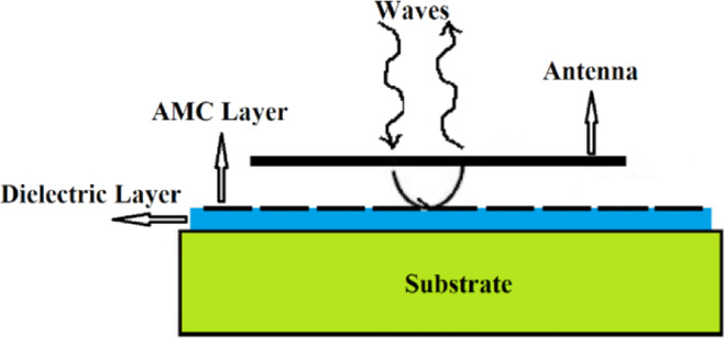
Wave incident on artificial magnetic conductor surface.
Reflection-coefficient of a plane TEM wave incident on Perfect Electric Conductor (PEC) is −1, which demonstrate that reflected wave will cancel the incident wave. On the other hand, the AMC plane indicates a reflection coefficient of +1, which means that the phase of the reflected wave is in phase of the incident wave. Therefore, with an AMC plane we can produce constructive phase reflections with the incident wave at across a finite operating frequency band. The consequence of this is enhanced radiation properties.
Numerous AMC structures have been explored to date in order to improve the radiation efficiency and bandwidth of on-chip antennas10–13, which includes proton implantation and micromachining14,15. These AMC structures require complex manufacturing steps and hence are highly expensive for mass production.
In this paper an artificial magnetic conductor (AMC) is designed using metasurface structure as a 2D composite right/left-handed (CRLH) metamaterial transmission line (TL), which was realized by etching concentric dielectric rings in the ground-plane of a polyimide substrate that are located under the radiating element comprising concentric metal rings constructed on the top substrate layer, as shown in Fig. 2. To accurately characterize the reflection phase of the incident wave on the metasurface structure a 3D full-wave EM solver based on finite element method (CST Microwave Studio) was used. The simulated reflection phase of the wave incident on the proposed AMC structure is compared with a conventional circular patch in Fig. 3. The results clearly show that with CRLH metamaterial-based AMC structure the reflection phase significantly drops and is around zero between 0.360 THz to 0.375 THz, which is a region where the losses are minimum and therefore optimum radiation achieved. The dispersion diagram of the proposed metamaterial structure in Fig. 2(b) is depicted in Fig. 4. It shows the negative group velocity is centered at around ωa/2πc = 0.3, which corresponds to approximately 365 GHz. The diagram reveals the range of the negative group velocity is approximately between 0.28 to 0.32.
Figure 2.
Geometry of the proposed AMC structure and the conventional circular patch. (a) Conventional circular patch radiator. (b) Proposed AMC consisting of concentric metal rings.
Figure 3.
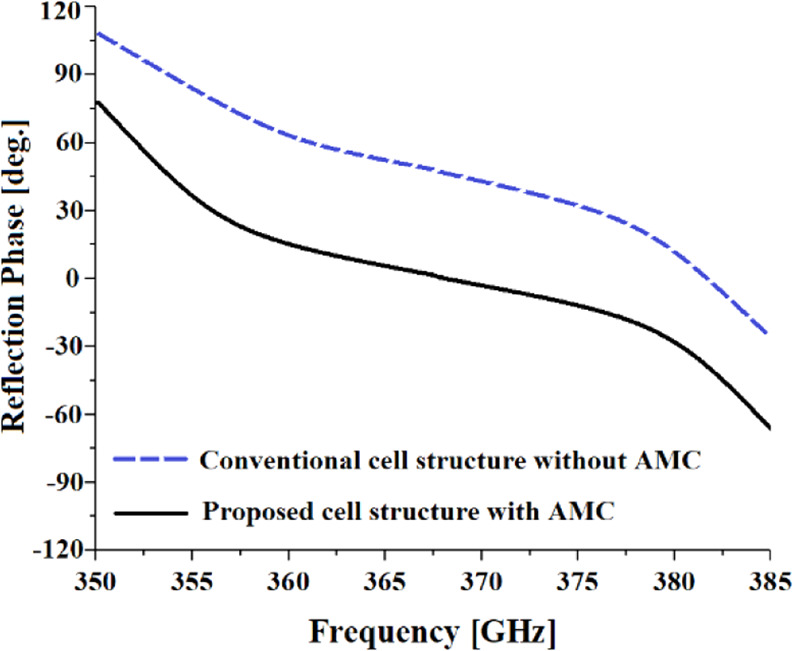
Reflection phase of the wave incident on AMC structure.
Figure 4.
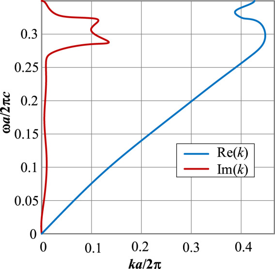
Real and imaginary parts of the dispersion diagram where k is the wave number and a is the gap between the radiation elements.
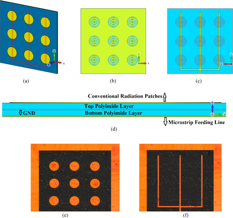
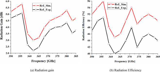
The proposed antenna was used to construct an antenna array comprising 3 × 3 circular radiating patches, as shown in Fig. 5. The array was constructed on two layers of polyimide stacked on top of each other where radiating elements are constructed on the top layer, the AMC structure constructed in the middle ground-plane layer, and the feeding network implanted in the underside of the bottom polyimide layer. Thickness of the polyimide substrate is 500 μm with a metallization layer of 3 μm thickness. The feedline is split in three open-ended branches that are located under the radiation elements. The antennas are excited by coupling electromagnetic energy through the gaps of the concentric dielectric rings using a microstrip feedline. The proximity between the feedline in the bottom layer and ground-plane causes image current to flow in the ground-plane that causes loss of energy in the form of heat. So, preferring CPW over microstrip line feeding is an excellent choice. Concentric dielectric rings in the ground-plane reduces substrate loss and suppresses surface waves which leads to enhanced bandwidth and radiation properties. The dimensions of the 3 × 3 antenna array shown in Fig. 5 is 6 × 6 × 1 mm3. The characteristics of the antenna was measured using a compact antenna test range as described in16. The simulated and measured reflection-coefficient responses of this antenna in Fig. 6 shows the antenna exhibits a bandwidth from 0.350 THz to 0.385 THz for S11 <−10 dB with a notch-band from 0.3575 THz to 0.3640 THz. Figure 7 shows the array’s measured radiation gain and efficiency vary from 2.2 dBi to 5.1 dBi and 40.34% to 51.67%, respectively, over its operating frequency band. The discrepancy between the measured and simulated results is attributed to the unknown dielectric loss-tangent of the polyimide layer over the frequency band of interest in the foundry’s design kit as well as unaccounted manufacturing tolerances.
Figure 5.
(a) Conventional circular radiation patches (yellow) on the top of the substrate and the CPW feedlines (red lines) on the underside of the bottom layer, (b) Concentric dielectric rings etched in the middle layer and located under the circular patches along with CPW open-circuited feedline located under the concentric dielectric rings, (c) back view of bottom layer showing CPW feedlines, and (d) cross-section of the antenna structure comprising two metallized polyimide layers, (e) Fabricated prototype, top view, and (f) Fabricated prototype, back view.
Figure 6.
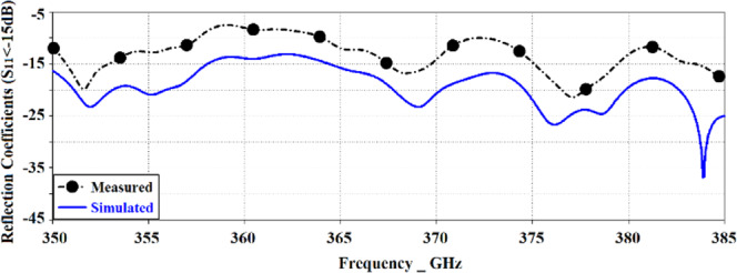
Simulated and measured reflection-coefficient responses of the proposed antenna array with circular patches.
Figure 7.
Simulated and measured radiation gain and efficiency of the antenna array with conventional circular patches as a function of frequency.
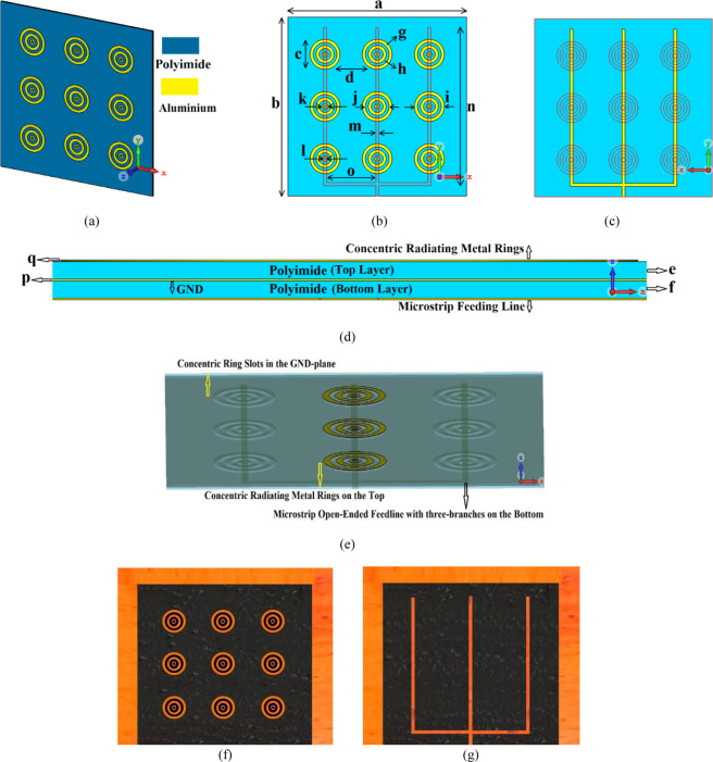
The circular radiation patches were replaced with concentric rings, as shown in Fig. 8. The dimensions of this structure are tabulated in Table 1. In this structure the concentric radiation rings essentially act as series left-handed capacitances (CL) that extend the effective aperture area of the antenna without affecting its dimensions and the concentric dielectric rings etched in the middle layer ground-plane act as shunt left-handed inductances (LL), which suppress the surface-waves and reduce the substrates losses that lead to improved bandwidth and radiation properties. The structure possesses the right-handed parasitic effects that can be seen as shunt right-handed capacitance (CR) and series right-handed inductance (LR). The shunt right-handed capacitance CR are mostly come from the gap capacitance between the patch and the ground plane, and the series right-handed inductance LR is created by unavoidable currents that flowing on the patches, which indicates that these capacitance and inductance cannot be ignored. Therefore, the overall structure behaves like a 2D composite right/left-handed (CRLH) metamaterial transmission line (TL) known as metasurface.
Figure 8.
(a) Isometric view of the on-chip antenna with AMC metasurface structure consisting of concentric radiation rings on the top of a standard polyimide substrate, (b) Concentric dielectric rings antennas (shown in yellow) in the middle layer and located under the concentric radiation rings along with CPW open-circuited feedline located under the concentric dielectric rings, (c) Back view showing the CPW feedline in ‘yellow’. The concentric dielectric rings (shown in red) are fabricated in the middle layer, (d) Cross-section view of the metasurface antenna containing two metallized polyimide layers, (e) Top view showing the concentric radiating metal rings in ‘yellow’, concentric dielectric ring slots in the middle layer, and CPW open-circuited three branched feed line on the underside of the bottom layer, (f) Fabricated prototype, top view, and (g) Fabricated prototype, back view.
Table 1.
Structural Parameters Of The On-Chip Antenna Array.
| Antenna’s size (a × b) | 6 × 6 mm2 |
| Circular patch (c) | 0.5 mm |
| Patch spacing (d) | 0.75 mm |
| Thickness of the polyimide layers (e & f) | 5 mm |
| Width of concentric metal rings (g) | 0.1 mm |
| Width of concentric ring slots (h) | 0.1 mm |
| Max. radius of concentric metal rings (i) | 0.5 mm |
| Max. radius of concentric ring slots (j) | 0.4 mm |
| Min. radius of concentric metal rings (k) | 0.1 mm |
| Min. radius of concentric ring slots (l) | 0.1 mm |
| Number of concentric metal rings | 3 |
| Width of feedline (m) | 0.1 mm |
| Length of feedline branches (n) | 5.3 mm |
| Space between the feedline branches (o) | 1.5 mm |
| Thickness of metallic conductor (p & q) | 0.003 mm |
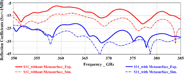
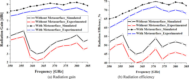
Figure 9 shows the antenna with metasurface structure exhibits a bandwidth from 0.350 THz to 0.385 THz for S11 <−20 dB. The average impedance match of this antenna with the metasurface is −30 dB that is almost two-fold than without the metasurface, which has an average impedance match of −12.5 dB. Figure 10. shows that the radiation gain and efficiency of the antenna change from 7.58 dBi to 8.65 dBi, and 60.85% to 72.47%, respectively. The average gain and efficiency are 8.15 dBi and 65.71%, respectively, which constitutes an improvement of 5 dBi and 20.42% when compared with no metasurface. The radiation properties are listed in Table 2. The results shows that, after apply the metasurface concept the effective aperture area of the on-chip antenna has extended and also the surface-waves and the substrates losses have suppressed without enhancing its dimensions17, which have caused to improve the on-chip antenna performance parameters such as impedance match, impedance bandwidth, radiation gain, and radiation efficiency.
Figure 9.
Simulated and measured reflection-coefficient responses of the proposed on-chip antenna ‘with’ and ‘without’ the metasurface.
Figure 10.
Simulated and measured radiation gain and efficiency curve plots of the proposed on-chip antennas ‘with’ and ‘without’ metasurface.
Table 2.
Measured radiation characteristics of the proposed on-chip antenna.
| Without Metasurface | With Metasurface | |
|---|---|---|
| Min. gain | 2.2 dBi | 7.58 dBi |
| Max. gain | 5.1 dBi | 8.65 dBi |
| Average gain | 3.15 dBi | 8.15 dBi |
| Average improvement | 5.0 dBi | |
| Min. efficiency | 40.34% | 60.85% |
| Max. efficiency | 51.65% | 72.47% |
| Average efficiency | 45.29% | 65.71% |
| Ave. improvement | 20.42% | |
In Table 3, the performance of the proposed on-chip antenna is compared with other types mm-waves and terahertz antennas recently publications. The comparison shows the proposed antenna operates at a much higher frequency and has comparable gain to18 but its efficiency is less. Its dimensions are larger than other antennas. However, the proposed antenna is less complex to implement. It is viable candidate for applications in terahertz integrated circuits.
Table 3.
Specifications of the proposed on-chip antenna compared with the literature.
| Refs. | Antenna Type | Frequency Band (GHz) | Gain (dBi) | Efficiency (%) | Dimensions (λ0 @ 350 GHz) | Process |
|---|---|---|---|---|---|---|
| 10 | Bowtie-slot | 90–105 | Max. −1.78 | — | 0.82 × 0.36 × 0.75 | IHP 0.13-μmBi −CMOS |
| 11 | Differential-fed circularly polarized | 50–70 | Max. −3.2 | — | 1.75 × 1.75 × 0.35 | 0.18-μm |
| 12 | Ring-shaped monopole | 50–70 | Max. 0.02 | Max. 35 | — | CMOS 0.18-μm |
| 13 | Circular open-loop | 57–67 | Max. −4.4 | — | 2.10 × 2.10 × 0.35 | CMOS 0.18-μm |
| 18 | Loop antenna | 65–69 | Max. 8 | Max. 96.7 | 0.81 × 1.45 | CMOS 0.18-μm |
| 19 | AMC embedded squared slot antenna | 15–66 | Max. 2 | — | 1.68 × 1.28 | CMOS 0.09-μm |
| 20 | Monopole | 45–70 | Max. 4.96 | — | 2.27 × 2.25 × 0.29 | Silicon CMOS |
| 21 | Dipole antenna | 95–102 | Max. 4.8 | — | — | Bi-CMOS |
| 22 | Tab monopole | 45–75 | Max. 0.1 | Max. 42 | 1.75 × 1.16 | Standard CMOS Silicon |
| 23 | Transmitter and receiver modules | 218–246 | Average 8.5 | — | 3.19 × 0.68 | 130-nm SiGe HBT Technology |
| 24 | Metamaterials and dielectric resonators | >450 | Max. 4.5 | Max. 45.7 | 0.46 × 0.46 × 0.15 | Standard CMOS |
| 25 | Monopole antenna | ~300 | Max. 1.72 | — | 0.35 × 0.35 × 0.09 | InP 50- μm Substrates |
| This paper | Metasurface & EM coupled feed mechanism | >350 | Min. 7.58 | Min. 60.85 | 7.0 × 7.0 × 1.16 | Standard 500-μm Polyimide |
Conclusion
A novel technique based on 2D CRLH metamaterial transmission line known as metasurface is described to design an antenna for on-chip applications operating at sub-terahertz frequency. The antenna was implemented on two layers of polyimide substrates using artificial magnetic conductor (AMC) structure. The antenna was excited using an open-circuited feedline located on the bottom polyimide layer where the electromagnetic signal is coupled to the antenna through the AMC structure. The AMC comprises concentric dielectrics rings constructed in the ground-plane sandwiched between the two-polyimide substrates, which has caused to suppress the surface waves and reduce substrates losses. The radiation elements located on the top polyimide layer are composed of concentric metal rings, which are realized based on the metasurface concept to extend the antenna effective aperture area. The antenna is relatively easy to manufacture and cost effective for mass production.
Acknowledgements
This work is partially supported by RTI2018-095499-B-C31, Funded by Ministerio de Ciencia, Innovación y Universidades, Gobierno de España (MCIU/AEI/FEDER,UE), and innovation programme under grant agreement H2020-MSCA-ITN-2016 SECRET-722424 and the financial support from the UK Engineering and Physical Sciences Research Council (EPSRC) under grant EP/E022936/1.
Author contributions
Conceptualization, M.A., B.S.V., F.F., and E.L.; methodology, M.A., B.S.V., C.H.S., E.L.; software, M.A., B.S.V., and C.H.S.; validation, M.A., C.H.S., R.A.A.-A., and F.F.; formal analysis, M.A., F.F., and E.L.; investigation, M.A., C.H.S., R.A.A.-A., and E.L.; resources, M.A., B.S.V., C.H.S., R.A.A.-A., F.F., and E.L.; data curation, M.A., C.H.S., and R.A.A.-A.; writing—original draft preparation, M.A.; writing—review and editing, B.S.V., C.H.S., R.A.A.-A., F.F., and E.L.; visualization, M.A., B.S.V., C.H.S., R.A.A.-A., F.F., and E.L.; supervision, E.L.; project administration, R.A.A.-A., F.F., and E.L.; funding acquisition, R.A.A.-A., F.F., and E.L.
Competing interests
The authors declare no competing interests.
Footnotes
Publisher’s note Springer Nature remains neutral with regard to jurisdictional claims in published maps and institutional affiliations.
Change history
8/7/2020
An amendment to this paper has been published and can be accessed via a link at the top of the paper.
References
- 1.Nascimento D. C. & Lacava J. C. S. Analysis and Design of Probe-Fed Linearly-Polarized Microstrip Antennas on FR4 Substrates. In IEEE Latin America Transactions, vol. 12, no. 6, pp. 965–970 (Sept, 2014).
- 2.Nascimento, D. C. & Lacava, J. C. S. Design of Arrays of Linearly Polarized Patch Antennas on an FR4 Substrate: Design of a probe-fed electrically equivalent microstrip radiator. IEEE Antennas and Prop. Magazine, vol. 57, no. 4, pp. 12–22 (Aug, 2015).
- 3.Laajimi, R. & Ajmi, A. Design of higher performance low power microstrip patch antenna with uniform supply used for UMTS applications. 2016 Int. Conference on Control, Decision and Information Technologies (CoDIT), St. Julian’s, pp. 308–312 (2016).
- 4.Alibakhshikenari, M. et al. Mutual Coupling Suppression Between Two Closely Placed Microstrip Patches Using EM-Bandgap Metamaterial Fractal Loading, IEEE Access, vol. 7, pp. 23606–23614, (March 5, 2019).
- 5.Alibakhshikenari, M., Virdee, B. S. & Limiti, E Compact Single Layer Travelling-Wave Antenna Design Using Metamaterial Transmission-Lines. Radio Science, Vol 52, pp 1510–1521, 10.1002/2017RS006313 (12 December 2017).
- 6.Mohammad Alibakhshikenari, B. S. et al. Limiti Study on Isolation Improvement Between Closely Packed Patch Antenna Arrays Based on Fractal Metamaterial Electromagnetic Bandgap Structures. IET Microwaves, Antennas & Propagation, Vol 12, 14, p. 2241–2247 (28 November 2018).
- 7.Mandal, S., Mandal, S. K. & Mal, A. K. On-Chip Antennas using Standard CMOS Technology: A Brief Overview. 2017 International Conference on Innovations in Electronics, Signal Processing and Communication (IESC), pp. 74–78, Shillong, India (6–7 April 2017).
- 8.Babakhani, A., Guan, X., Komijani, A., Natarajan, A. & Hajimiri, A. A 77-GHz phased-array transceiver with on-chip antennas in silicon: Receiver and antennas. IEEE J. Solid-State Circuits, vol. 41, no. 12, pp. 2795–2806 (Dec.2006).
- 9.Elsheakh, D. M., Elsadek, H. A. & Abdallah, E. A. Antenna Design with Electromagnetic Band Gap Structures. INTECH Open Access Publisher (2012).
- 10.Khan, M. S., Tahir, F. A. & Cheema, H. M. Design of bowtie-slot on-chip antenna backed with E-shaped FSS at 94 GHz. 2016 10th European Conference on Antennas and Propagation (EuCAP), Davos, pp. 1–3 (2016).
- 11.Wang, L. & Sun, W. Z. A 60-GHZ differential-fed circularly polarized on-chip antenna based on 0.18-m COMS technology with AMC structure. IET International Radar Conference 2015, Hangzhou, pp. 1–4 (2015).
- 12.Huang, H. T., Yuan, B. & Zhang, X. H. A circular ring-shape monopole on-chip antenna with artificial magnetic conductor. 2015 Asia-Pacific Microwave Conference (APMC), Nanjing, pp.1–3 (2015).
- 13.Bao, X. Y., Guo, Y. X. & Xiong, Y. Z. 60-GHz AMC-Based Circularly Polarized On-Chip Antenna Using Standard 0.18-m CMOS Technology. IEEE Transactions on Antennas and Propagation, vol. 60, no. 5, pp. 2234–2241 (May 2012).
- 14.zhang, Y. P. & Duixian. Antenna-on-chip and Antenna-in-Package Solutions to Highly Integrated millimeter-Wave Devices for Wireless Communications. IEEE Transactions on Antennas and Propagation, vol. 57, no. 10, pp. 2830–2841 (October 2009).
- 15.Hoivik, N., Liu, D. & Jahnes, C. V. High-efficiency 60 GHZ antenna fabricated using low-cost silicon micromachining techniques. In Antennas and Propagation Society International Symposium, IEEE, pp. 5043–5046 (2007).
- 16.Liu C, Wang X. Design and Test of a 0.3 THz Compact Antenna Test Range. Prog. Electromagn. Res. Letters. 2017;70:81–87. doi: 10.2528/PIERL17080504. [DOI] [Google Scholar]
- 17.Christophe, C. & Itoh, T. Electromagnetic Metamaterials: Transmission Line Theory and Microwave Applications, ISBN: 978-0-471-66985-2, 376 pages, Wiley-IEEE Press (November 2005).
- 18.Song, Y., Wu, Y., Yang, J. & Kang, K. The design of a high gain on-chip antenna for SoC application. Advanced Materials and Processes for RF and THz Applications (IMWS-AMP), 2015 IEEE MTT-S Int. Microwave Workshop Series on, Suzhou, pp. 1–3 (2015).
- 19.Lin, F. & Ooi, B. L. Integrated millimeter-wave on-chip antenna design employing artificial magnetic conductor. 2009 IEEE International Symposium on Radio-Frequency Integration Technology (RFIT), Singapore, pp. 174–177 (2009).
- 20.Upadhyay, S. & Srivastava, S. A 60-GHz on-chip monopole antenna using silicon technology. Applied Electromagnetics Conference (AEMC), 2013 IEEE, Bhubaneswar, pp. 1–2 (2013).
- 21.Nafe, M., Syed, A. & Shamim, A. Gain enhancement of low profile on-chip dipole antenna via Artificial Magnetic Conductor at 94 GHz. 2015 9th European Conference on Antennas and Propagation (EuCAP), Lisbon, pp. 1–3, (2015).
- 22.Yang, W., Ma, K., Yeo, K. S. & Lim, W. M. A 60 GHz on-chip antenna in standard CMOS silicon Technology. Circuits and Systems (APCCAS), 2012 IEEE Asia Pacific Conference on, Kaohsiung, pp. 252–255 (2012).
- 23.Grzyb, J. et al. High data-rate communication link at 240 GHz with on-chip antenna-integrated transmitter and receiver modules in SiGe HBT technology, 11th European Conference on Antennas and Propagation (EUCAP), pp. 1369–1373 (19–24 March 2017).
- 24.Alibakhshikenari, M., Virdee, B. S., See, C. H., Abd-Alhameed, R. A. & Limiti, E. Silicon-based 0.450-0.475 THz series-fed double dielectric resonator on-chip antenna array based on metamaterial properties for integrated-circuits. 13th Int. Congress on Artificial Materials for Novel Wave Phenomena - Metamaterials 2019, pp. 26–28 (16–21 September 2019).
- 25.Guo, L., Deng, M., Zhang, Q., Zhang, X. & Yuan, Z. Dual-polarized on-chip antenna for 300 GHz full-duplex communication system. Hindawi International Journal of Antennas and Propagation, Vol. 2017, Article ID 2837629, 7 pages, 10.1155/2017/2837629.


