Abstract
The unique flexible and piezoelectric properties of polyvinylidene fluoride (PVDF) films would allow for new applications for integrated bioelectronic devices. The use of these films has been precluded by the difficulty in machining them into small, discrete features without damaging the properties of the material. The etching of piezoelectric PVDF by means of a 193 nm excimer laser is explored and characterized. Etch rates are shown for common laser fluence values, along with images of the quality of the cuts to provide the reader with an understanding of the compromise between etch rate and edge roughness. The authors describe a novel method for the etching of piezoelectric, -phase PVDF. While PVDF is flexible, acoustically matched to biological tissue, and has a wide resonance bandwidth, it is often overlooked as a piezoelectric material for micro-electrical-mechanical-system devices because of the difficulty in fabrication. In this paper, the authors characterize the etch rate and quality while using a 193 nm argon fluoride excimer laser for patterning.
I. INTRODUCTION: THE NEED FOR PVDF
Piezoelectric devices are used in a variety of applications from simple microphones, to actuators, to more complex ultrasonic transducers. Traditionally, piezoceramics such as lead zirconium titanate (PZT) have filled these roles because of their high electromechanical coupling factor. However, piezoelectric polymers have recently gained attention by bringing unique material properties that provide advantages for many applications.
In comparison to ceramics, polyvinylidene fluoride (PDVF) has the ability to flex and conform to a shape. This is useful in biological applications to either make good contact with the curvature of the skin or to minimize foreign-body responses when implanting a PVDF device. Moreover, PVDF is biocompatible, chemically inert, and lead-free.
PVDF has an acoustic impedance of 2.5 MRayls in comparison to 33.7 MRayls for PZT-5H.1 This implies that if a transducer made of each of these materials is transmitting or receiving directly into water, 6.6 and 85.1 of the pressure from PVDF and PZT-5H are reflected, respectively. The piezoelectric coupling coefficient, , of PVDF is only 0.27 compared to 0.69 for PZT. Thus, most of the PZT signal is lost if a matching layer is not added (requiring additional fabrication stages).2
A. State of the art PVDF machining methodologies
As a fluoropolymer, PVDF is inherently difficult to micromachine. It is chemically inert, making it resistant to most wet etching processes. In order to maintain the piezoelectric properties of -phase PVDF, processing temperatures must be kept below C. This requires the development of nontraditional photolithography techniques in order to create photoresist masks for selective etching.
Han et al. reported high etch rates of PVDF using N,N-dimethylacetamide. At C, an etch rate of nm/min was achieved.3 This increases to 40 000 nm/min at C. Unfortunately, this etch is isotropic, making high-aspect ratio features impossible. Moreover, etch mask selectivity can be a problem, as strong organic solvents attack both photoresists and bonding materials easily.
Dry etching using reactive ion etching (RIE) techniques allows for a degree of anisotropicity, which is necessary for tall, high-aspect ratio pillars commonly found in many applications of piezoelectric materials. Miki et al. achieved an etch rate of 167 nm/min with an etch chemistry of .4 Later experiments involving increased concentrations allowed for etch rates as high as 667 nm/min. However, this higher vertical etch came at the cost of a horizontal etch rate of 1333 nm/min, making high-aspect ratio features impossible.5 Lower rates were obtained with a similar etch chemistry at a lower power.3 Substantially higher etch rates of near 770 nm/min were reported when using a combination of and chemistries.6 While the features show sharp sidewalls, the comparatively slow etch rate prohibits the creation of tall features greater than 100 in height. In addition to the gas species concentration, the masking material has a significant effect on sidewall angle. Shi et al. used a photoresist mask to obtain a gentle sloped sidewall for easier metal deposition for the top metal contact of fabricated features.7
Attempts have been made to micropattern features into PVDF using laser irradiation. Lee et al. used a 775 nm Ti:Sapphire femtosecond laser to etch metalized PVDF. At this long wavelength, gas bubbles formed from released during polymer decomposition, and significant thermal effects were noted.8 Liu and Jiang used a 248 nm laser to selectively increase resistivity through surface modification. However, the fluence of the particular laser was not high enough for machining and separation of the PVDF into freestanding pillars.9
Success has been shown using extreme ultraviolet (EUV) sources to etch PVDF in a clean and controlled manner. Bartnik et al. used a 10 Hz, 11 nm laser-plasma source to focus a 60 mJ/cm beam on PVDF, producing very clean sidewalls for depths of 50 . Unfortunately, the etch rate is very slow at 70 nm/pulse, or 42 000 nm/min for a spot.10 Such a method provides excellent sidewall quality and resolution, but EUV sources are rare, and the etch rate may be prohibitively slow for tall features.
B. Excimer laser ablation
Excimer lasers operate in the UV spectrum, providing high photon energy to break chemical bonds. Unlike traditional lasers that use thermal ablation mechanisms to vaporize a material, excimer lasers use a photoablative effect to break chemical bonds, allowing for the removal of the resulting smaller particles.11
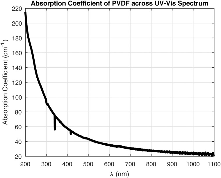
Argon fluoride (ArF) lasers emitting at 193 nm are regularly used to cleanly ablate glass, ceramics, and organic tissue with superior quality in comparison to high-power machining lasers at longer wavelengths. Moreover, PVDF has a higher absorption coefficient at shorter wavelengths, as shown in Fig. 1, allowing for efficient use of the beam energy.
FIG. 1.
Measured UV–Vis absorption spectrum of -phase piezoelectric PVDF.
The two major mechanisms used to describe the laser removal of material are photothermal ablation (often referred to as thermal ablation) and photochemical ablation (often referred to as photoablation). In thermal ablation, the absorbed energy penetrates to a given depth determined by the material’s absorption coefficient, causing the material to heat up, ultimately vaporizing. Provided that the photon energy is greater than the bond strength, photoablation may occur. This process uses the photon energy directly to break chemical bonds, vaporizing the shorter polymer molecules.11 As some heat is still transferred to the surface, most ablation processes contain some thermal effects.12 An advantage of ArF lasers is the high photon energy of about 6.42 eV, in comparison to 1.6 eV for a femtosecond Ti-sapphire femtosecond laser.8,11 This high photon energy allows for the breaking of C–C (3.90 eV), C–H (3.51 eV), and C–F (4.99 eV) in PVDF without resorting to melting the material, as one would find with lower energies.13,14
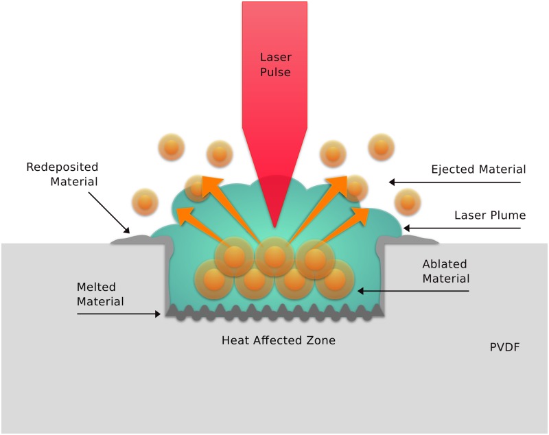
Although surface modification and limited etching can occur at low energy fluences, polymers begin to ablate quickly above a fluence value known as the threshold fluence. This value depends on the material as well as the applied wavelength, but tends to fall in the low mJ/cm range. For example, the ablation threshold of polyimide at 193 nm is 15 mJ/cm.12 As the fluence increases, a plasma plume is generated over the surface. This plume can partially shield the material underneath it, preventing higher fluences from linearly increasing the etch rate. If there is not enough energy to vaporize a material, some may melt, and the pressure generated by the plasma plume above may result in the resettling of this molten material in the newly generated crater. This is generally undesirable, as it results in a rough surface, where clean material removal is desired. Below this is the so-called heat affected zone. The depth of this zone is , which, for PVDF, given a thermal diffusivity of cm/s, should only be nm.15 In reality, this is much larger due to the addition of thermal ablative effects from the residual energy not being used to break bonds. A conceptual illustration of this combined material removal process and the shielding plasma plume is shown in Fig. 2.
FIG. 2.
Demonstration of laser ablation and the resulting plasma plume on the surface of a material. Figure is not to scale.
As excimer lasers rely on the excitation of a pair of rare gas halides, a limiting factor of excimer lasers is the ns excitation duration before the gas species return to a relaxed state.11 This fundamentally limits the pulse duration to orders of magnitude longer than femtosecond lasers. A longer pulse duration allows for greater heating of the machined material, possibly causing unwanted melting and surface chemical changes.8 This effect is mitigated by greater coupling to the material at lower wavelengths, resulting in more material decomposition and less melting.
II. EXPERIMENT
A piece of 110 , prepoled, -phase PVDF was cut from a commercially purchased sheet (Kureha).16 This piece of PVDF was measured to have a piezoelectric coefficient of 21 pC/N using a PiezoTest PM300 meter prior to any processing. We can use the relation , where is the elastic compliance and is the dielectric constant of the PVDF, to find the to be 0.11.
To secure the sample to a flat working surface, a polished 300 -thick Si wafer was used as a substrate. The side of the PVDF to be bonded was pretreated in an Anatech Plasma asher flowing 100 SCCM of at 100 W of forward power for 3 min. This chemically activates the surface of the fluoropolymer, making it amenable to permanent bonding. Microchem SU-8 3005 was directly applied to the Si wafer and spin coated at 4000 rpm for 45 s to provide an approximately 5 -thick layer. This was then exposed in a Karl Suss MA6 mask aligner at 100.8 mJ/cm. The plasma-treated side of the PVDF is placed face-down onto the SU-8 coated Si wafer. A Finetech Lamda Fineplacer is then used to apply heat and pressure to finish the cross-linking process. The Fineplacer applied 68.75 N/cm of pressure while simultaneously heating the stack to C for 30 min. This fully cures the SU-8, creating a permanent bond to the wafer and a flat PVDF surface for laser ablation.
An IPG IX-255 excimer laser system was used to etch the PVDF. The system uses an ArF 193 nm laser capable of providing fluences in excess of 25 J/cm for pulse durations of approximately 10 ns. To characterize the material, test grids were exposed, where a constant pulse repetition rate and spot size were used for each grid. Two sets of apertures were used for this experiment, resulting in a 50 50 spot size and a 70 70 spot size. Both are formed by masking the beam through a rectangular variable aperture. The smaller spot size is more uniform across the entire beam area, but the larger spot size can provide faster etching when cutting lines or rastering areas. This experiment was repeated for pulse repetition rates of 50, 100, and 500 Hz.
Each of the test grids had six rows and 31 columns. The rows correspond to the number of test shots: 5, 10, 25, 50, 75, and 100 shots, respectively. In this context, a shot is a single pulse of approximately 10 ns that is fired by the laser. When multiple shots are fired, they are striking the same area and effectively drilling down into the material, leaving a square hole. At high pulse repetition rates, the higher shot counts will exhibit greater thermal effects. Each column represents a different energy fluence value, modified by changing the variable attenuator (VAT). The VAT is a coated optical blade that is partially inserted into the beam path to attenuate the fluence based on the amount inserted. The VAT angle was varied from to (corresponding to 21.2 J/cm down to 2.2 J/cm), respectively, in steps of . The corresponding power is then measured using an Ophir power meter to calculate the energy fluence of each point.
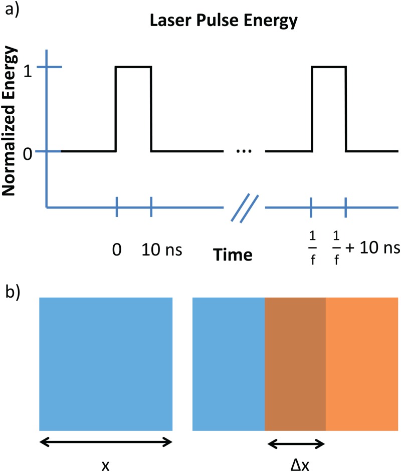
Many etching applications require the machining of lines or traces as opposed to individual points. To help characterize the machinability of piezoelectric PVDF using a 193 nm laser, additional test grids were made of 500 -long lines, using the 50 50 spot size. For the case of linear exposures, the concept of shot overlap is introduced to control edge quality. Here, the overlap is defined as the percentage of the area a previous shot shares with the area of the next pulse. Drilling holes has an overlap of 100 because each shot is exactly placed over the area of the last one without moving in the lateral dimensions. The temporal pulse duration and the overlap ratio are illustrated in Fig. 3.
FIG. 3.
(a) Normalized energy of each energy pulse. The spacing between pulses is determined by the repetition rate, . (b) Top view of a single and two consecutive shots. If the beam width is given by and the overlap is given by , then the overlap percentage is .
For this test grid, each row corresponds to the amount of overlap between shots as opposed to a number of shots. All lines were scanned with an energy density of 8.32 J/cm. The overlap varied from 0.5 /shot (99 overlap) to 10 /shot (80% overlap).
Direct measurement of the etch depth of the holes in the PVDF is complicated by the aspect ratio and rough surface quality at the bottom of these etched areas. Surface morphology is an inexact determinant. Depending on the fluence and number of pulses fired, the surface could be scarred by incubation heating, i.e., no perceivable etched depth, but the surface is roughened by 1–5 . In the other extreme, the etched hole could be deeper than 110 , implying the laser removed all of the PVDF and some of the underlying cured SU-8 and silicon. The bottom of these holes can have a surface roughness comparable to the underetch case, depending on the repetition rate. Measuring these 50 50 cavities with a comparably sized profilometer tip leads to the probe bottoming out and an underestimate of the actual depth. Optical profilometry fails to measure this correctly as the intensity of light that returns from each hole is over 1000 times weaker than that reflected by the surface because of scattering of light at the bottom of each hole.
To circumvent these issues, the etched pillars were measured indirectly by creating an inverse Sylgard 184 polydimethylsiloxane (PDMS) mold of the etched structures. A 3D-printed 2 2 cm hollow square enclosure was used to create a dam for the PDMS. It was mounted directly on the PVDF sample, centered around the test area, and the bottom was sealed using silicone to prevent PDMS from leaking. The fenced-in area was then filled with approximately 4 ml of PDMS, desiccated for 30 min, and allowed to cure at C for 2.5 h. The PDMS was then manually removed from the mold to produce a freestanding 2 2 1 cm PDMS block with pillars imprinted in the same shape and size of the holes on the PVDF. The heights of each of these pillars were then measured using a Bruker Dektak-XT stylus profiler.
III. RESULTS AND DISCUSSION
For a pure photochemical ablation process, the expected etch rate should follow the Beer–Lambert law,
| (1) |
where is the etch rate in micrometers per pulse, in cm is the absorption coefficient of the material, is the applied fluence in J/cm, and is the threshold fluence.
The optics path of the beam delivery system for the laser workstation was not configured to apply low fluence pulses. This precludes testing close to the ablation threshold of PVDF, which is expected to be on the order of hundreds of mJ/cm. For example, at 775 nm, Lee et al.8 found the so-called “damage threshold” of PVDF to be 156 mJ/cm. The poor coupling of the beam to the PVDF is even seen at 193 nm. For smaller 50 50 spot sizes, the surface morphology is rough at lower repetition rates where thermal effects are less of a factor. The bottom surface of these rough trenches translates into rough pillars after making the PDMS mold. These data points have the greatest variance.
A. Etching single spots
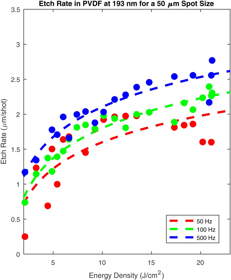
As seen in Fig. 4, the measured etch rate of PVDF follows the Beer–Lambert law and starts to become more linear far from the threshold fluence. One can create a logarithmic fit based on Eq. (1), and extract and . If one extrapolates the threshold fluence from the fit, the average threshold fluence when using a 50 50 spot size is 467 mJ/cm, which is considerably higher than reported for 775 nm. The absorption coefficient was measured to be 1.69 cm, but this simplified model does not take into account the change in absorption under irradiation.
FIG. 4.
Etch rate of PVDF for a 50 50 spot size for various pulse repetition rates.
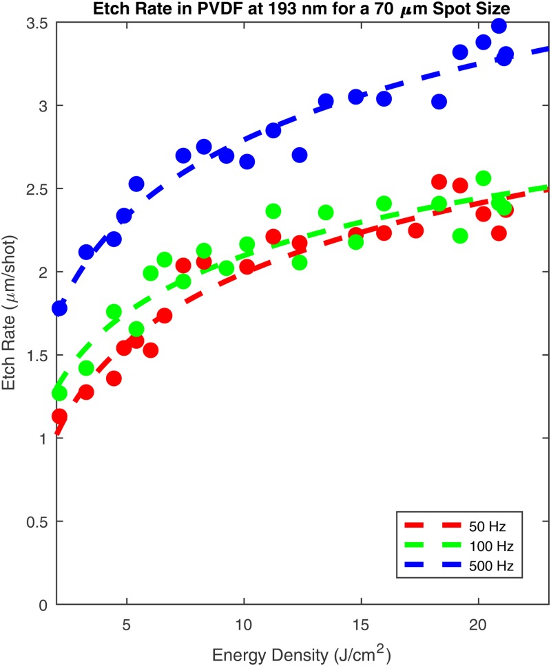
As a smaller spot size is produced by masking the main beam, it should provide a more uniform beam profile. However, the resulting smaller pillars had a consistently lower etch rate than for a 70 70 spot size, as shown in Fig. 5. Here, the average threshold fluence was 219 mJ/cm, with an absorption coefficient of 1.73 cm. The larger spot size increased the etch rate by approximately 25. This suggests that smaller spot sizes with higher aspect ratio holes are rate-limited by the ability to remove material from the narrow trench. It is also important to note the large increase in the etch rate between the 100 and 500 Hz repetition rates, indicating a transition to a more thermal ablative mechanism as there is less time to cool between pulses.
FIG. 5.
Etch rate of PVDF for a 70 70 spot size for various pulse repetition rates.
B. Etching lines
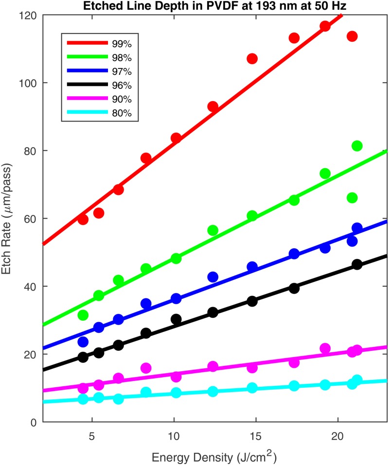
Figure 6 illustrates the increase in the etch rate with increasing levels of shot overlap. As expected, a greater overlap will expose a given area to a greater number of shots, thus increasing the total amount of material removed per pass.
FIG. 6.
Etch rate vs energy density with a 50 50 beam at 50 Hz for various levels of shot overlap.
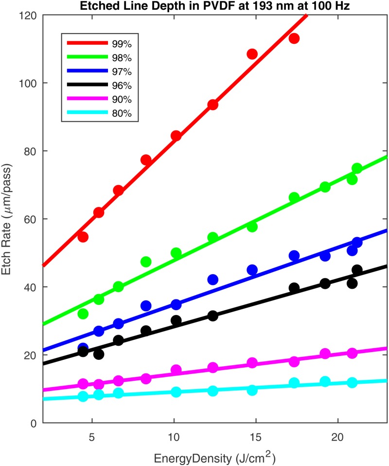
A higher pulse repetition rate is often desirable to improve throughput in patterning large areas. In Fig. 7, one can maintain ablation rates at 100 Hz that are comparable to those achieved at 50 Hz. One important outlier is the 99 overlap scenario, implying that the close pulse spacing of 0.5 is dense enough to start to cause thermal ablation or melting. A closer examination of the surface topology is presented later in this section.
FIG. 7.
Etch rate vs energy density with a 50 50 beam at 100 Hz for various levels of shot overlap.
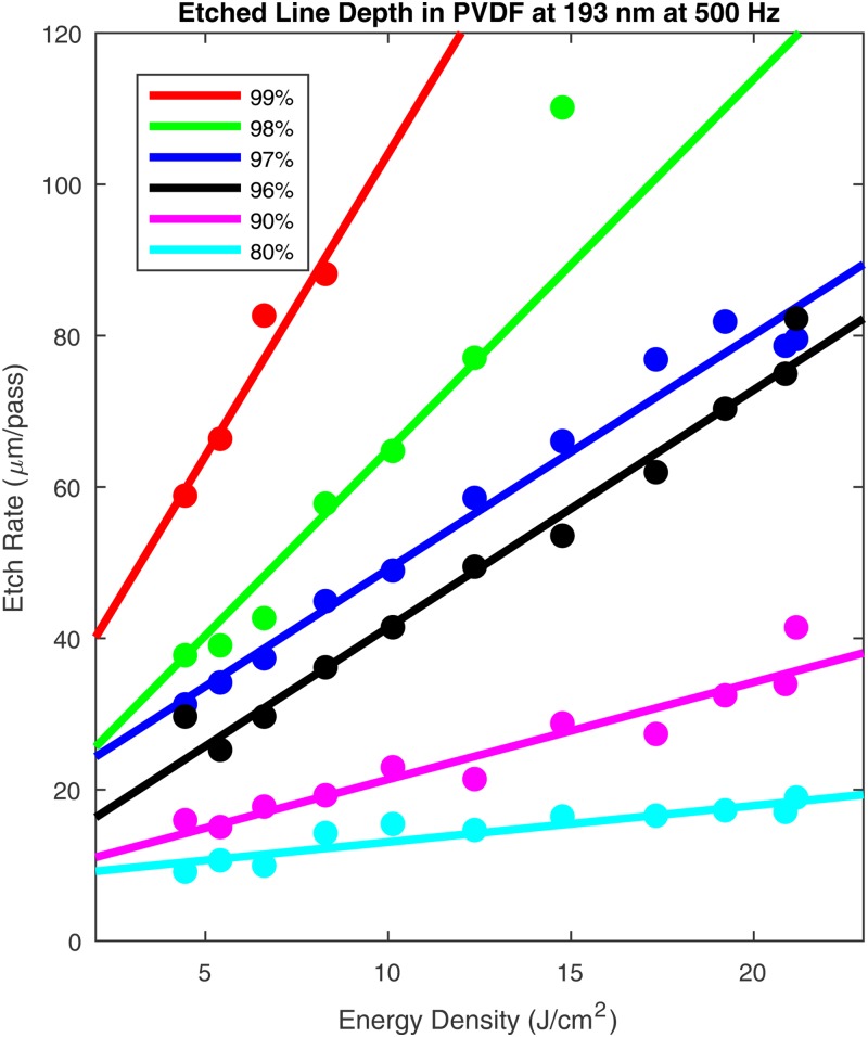
Increasing the pulse repetition rate even further to 500 Hz, as shown in Fig. 8, demonstrates that the etch rate rapidly increases. For high overlap ratios, the entire 110 -thick PVDF sheet was completely etched through, even at moderate fluence values of 14 J/cm. However, at lower overlap ratios, a more linear increase in the etch rate with fluence is observed. This may also be a result of the now-moving plasma plume generated across the surface of the etched material. With close overlap, the force exerted by the plume directly above the irradiated area may prevent material from escaping the ablation zone. This results in the area retaining heat, causing additional melting in the region.
FIG. 8.
Etch rate vs energy density with a 50 50 beam at 500 Hz for various levels of shot overlap.
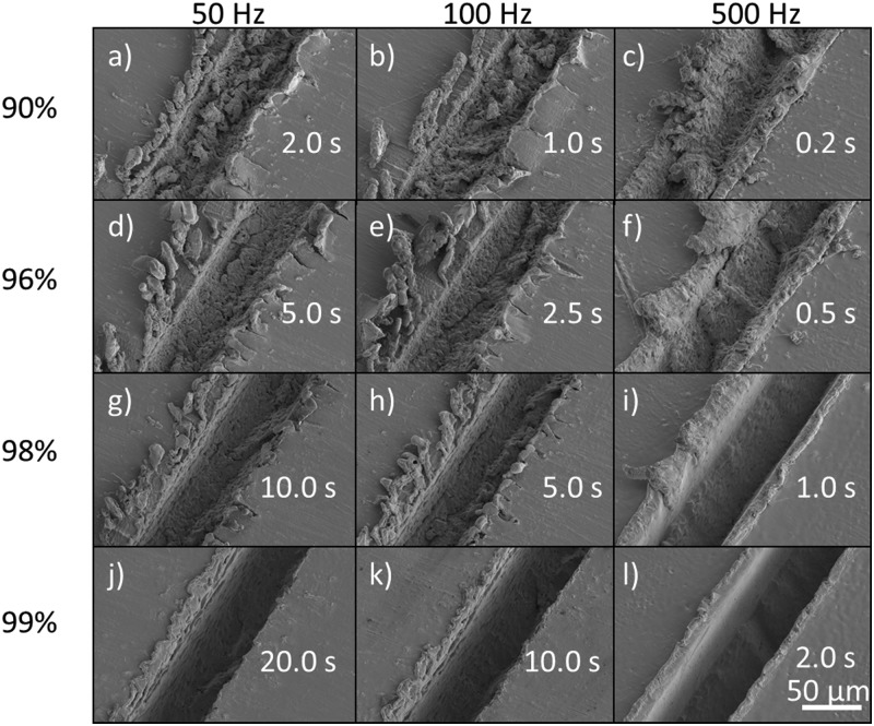
One of the main advantages of using an excimer laser for PVDF ablation is the trade-off achievable between the etch rate and the edge quality. As previously mentioned, dry etching through RIE can provide vertical sidewalls, but the throughput is severely limited by the poor etch rate. Faster etch rates can be obtained with wet etching, but patterning fine features is difficult. Lasers at longer wavelengths burn the PVDF, depolarizing it. As seen in Fig. 9, a compromise can be made with an excimer laser between the overlap amount and the quality. For the purpose of comparison, a fixed fluence of 8.32 J/cm was chosen as a point well above the threshold fluence. Similar results are seen for various fluences, corresponding to the previously demonstrated etch rates.
FIG. 9.
SEM images of single passes of a 50 50 beam at 8.32 J/cm. The approximate processing time for the given conditions is shown in each panel. The scale bar applies for all panels.
High repetition rates allow for faster processing, resulting in more removed material per pass. However, as the material is removed in discrete steps, this may lead to overshooting on a specific target depth. This can be mitigated by doing several passes at higher repetition rates, to remove most of the material, and slowing to a lower etch rate as finer depth control is needed. While an increased repetition rate and overlap percentage provide higher edge quality, it allows less time for cooling in the localized area, potentially causing melting on the sidewalls. This reflow of material is likely the cause of the smooth wall profile at 99 overlap.
For low levels of shot overlap, a coarser line texture is observed. This can be partially overcome with multiple passes, which effectively mimics closer pulse spacing. Closer pulse spacing provides an advantage of a deeper trench, and more vertical sidewalls. Moreover, increasing the repetition rate can lead to localized melting near the edges of the PVDF. This happens on the micrometer scale, which does not affect the PVDF tens of micrometers from the ablation area, but does provide a smooth surface where the fibrous texture of the PVDF is less noticeable. Moreover, higher repetition rates generally translate to greater throughput.
C. Creating square features
In Secs. III A and III B, we have shown that it is possible to both drill holes and cut trenches in the PVDF. This can further be expanded to create features of arbitrary shapes. Given the small beam size compared to a working PVDF surface that could potentially measure several centimeters, it is more efficient to simply trace the outline of proposed features as opposed to rastering away the entire unwanted area.
An approximately 1 m-thick layer of Perminex 2001 adhesive was spin coated at 3000 rpm for 30 s on a 1 mm-thick glass slide. Perminex was used to improve bonding and thus improve pillar yield.17 The solvent was evaporated by a bake at C for 5 min. This substrate was then exposed using the MA6 mask aligner with a photomask that exposed only 425 425 squares arranged in a 16-by-16 grid. The PVDF was exposed to the same plasma treatment as the previous experiments to improve adhesion. It was then bonded to the Perminex sample using the Fineplacer with 100 N/cm, while baking the stack at C for 2 min. The excimer laser was then used to trace around the perimeter of the exposed squares, as the Perminex should only form bonds in these areas. In all cases, multiple passes were required to cut completely through the PVDF. After each pass with given parameters, the beam was manually focused down onto the newly exposed surface in the trench. The process was repeated until the PVDF was entirely etched through. After etching, the remaining bulk PVDF was manually peeled off with tweezers, and the resulting pillars were cleaned with acetone.
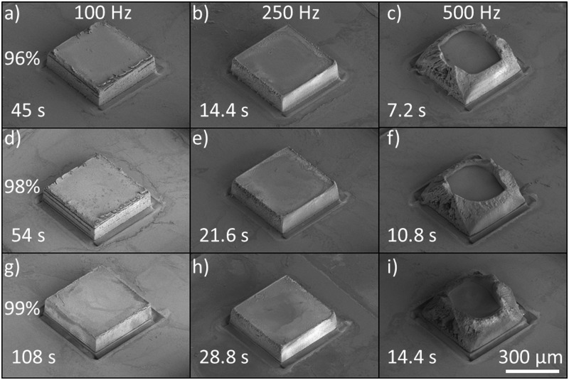
Selected features are shown in Fig. 10. As expected, both higher repetition rates and greater overlap ratios resulted in greater melting of the material. Lower repetition rates resulted in voids opening along the length of the PVDF, as seen in Figs. 10(a) and 10(d). Conversely, at a repetition rate of 500 Hz, substantial thermal damage and redeposition of material are apparent, as illustrated by Figs. 10(f) and 10(i). Lower overlap ratios were not included as strands of PVDF would remain, requiring over 12 passes per pillar. Even under these conditions, those pillars would not always survive the peeling process as fibers of PVDF still would hold the feature to the excess PVDF.
FIG. 10.
SEM images of 425 425 PVDF features etched using a 50 50 beam at 8.32 J/cm. The approximate processing time for the given conditions is shown in the bottom-left corner of each panel. The percentage of shot overlap for each row is shown to the left, the repetition rate used for each column is shown at the top. The scale bar applies for all panels.
As with etching lines, increasing the pulse repetition rate and decreasing the overlap allow for an individual pass to be completed in less time. However, this does not always equate to a greater throughput, as less material is removed per pass. The etch rates determined in Figs. 6 and 8 can be used to accurately approximate the amount of etched material per pass. For example, using a 96 overlap at 100 Hz as in Fig. 10(a) requires five passes to go through all 110 of PVDF, but using 99 overlap at 500 Hz as in Fig. 10(j), only requires two passes. In all cases, there was some level of overshoot that was intentionally done to ensure that the final pass went entirely through the PVDF. To avoid damaging the substrate, it may be advantageous to etch the final steps at a lower power, but this would require tuning to the specific application. In terms of having the most vertical sidewalls with the least debris, a repetition rate of 100 Hz with a 99 shot overlap ratio is preferred. However, a 7.5-fold increase in throughput can be achieved with minimal decrease in quality by using a 250 Hz repetition rate with a 96 shot overlap ratio. Higher repetition rates cause excessive melting and damage to the PVDF.
IV. CONCLUSION
A 193 nm ArF excimer laser was used to ablate piezoelectric PVDF. The potential for the use of such a laser for the patterning of micromachined piezoelectric transducer structures was investigated. This was accomplished by the characterization of the etch rate and fitting to a Beer–Lambert model, allowing for the extraction of an approximate absorption coefficient and threshold fluence for the material.
Both individual shots and etched lines were separately investigated. Individual shots allow for the more direct characterization of the laser interaction with the material. Practically, this allows for the drilling of high-aspect ratio holes, potentially for electrical vias or other connections. Etched lines are shown to provide a guide to the expected etch rate for various overlap ratios, energy densities, and pulse repetition rates. This information was then applied to the patterning of square PVDF features. These could then potentially be used to form individual transducers or cantilevers. A trade-off between edge quality and fabrication throughput was noted to depend on pulse repetition rate.
ACKNOWLEDGMENTS
The authors wish to acknowledge the support of Tiago Costa for his advice on measurement techniques as well as IPG Photonics for their technical suggestions on the operation of the excimer laser. In addition, the authors would also like to thank Jakub Jadwisczak for his advice and support in the preparation of this manuscript. This work was performed, in part, at the Advanced Science Research Center NanoFabrication Facility of the Graduate Center at the City University of New York.
REFERENCES
- 1.NSF-ATE, NDT Resource Center.
- 2.Ramadan K. S., Sameoto D., and Evoy S., Smart Mater. Struct. 23, 033001 (2014). 10.1088/0964-1726/23/3/033001 [DOI] [Google Scholar]
- 3.Han H., Nakagawa Y., Takai Y., Kikuchi K., Tsuchitani S., and Kosimoto Y., J. Micromech. Microeng. 22, 1–8 (2012). 10.1088/0960-1317/22/8/085030 [DOI] [Google Scholar]
- 4.Miki H., Matsui G., Kanda M., and Tsuchitani S., J. Micromech. Microeng. 25, 035026 (2015). 10.1088/0960-1317/25/3/035026 [DOI] [Google Scholar]
- 5.Miki H., Sugii R., Kawabata Y., and Tsuchitani S., IEEJ Trans. Electr. Electron. Eng. 14, 1575 (2019). 10.1002/tee.22978 [DOI] [Google Scholar]
- 6.Miki H., Morimoto K., Tamaki T., and Tsuchitani S., Int. J. Eng. Tech. Res. 3, 327 (2015). [Google Scholar]
- 7.Shi C., Costa T., Elloian J., and Shepard K. L., Technical Digest—International Electron Devices Meeting (IEDM’2018), San Francisco, CA, 1–5 December 2018 (IEEE, San Francisco, CA, 2019), p. 4.5.1 [Google Scholar]
- 8.Lee S., Bordatchev E. V., and Zeman M. J. F., J. Micromech. Microeng. 18, 045011 (2008). 10.1088/0960-1317/18/4/045011 [DOI] [Google Scholar]
- 9.Liu Y. and Jiang Y., Opt. Express 18, 22041 (2010). 10.1364/OE.18.022041 [DOI] [PubMed] [Google Scholar]
- 10.Bartnik A., Fiedorowicz H., Jarocki R., Kostecki J., Szczurek M., and Wachulak P. W., Appl. Phys. A Mater. Sci. Process. 106, 551 (2012). 10.1007/s00339-011-6662-z [DOI] [Google Scholar]
- 11.Shrikrishna J. and Dixit N., Lasers Based Manufacturing, Topics in Mining, Metallurgy and Materials Engineering, edited by S. N. Joshi and U. S. Dixit (Springer India, New Delhi, 2015).
- 12.Bityurin N., Luk’yanchuk B. S., Hong M. H., and Chong T. C., Chem. Rev. 103, 519 (2003). 10.1021/cr010426b [DOI] [PubMed] [Google Scholar]
- 13.Blanksby S. J. and Ellison G. B., Acc. Chem. Res. 36, 255 (2003). 10.1021/ar020230d [DOI] [PubMed] [Google Scholar]
- 14.Luo Y.-R., Comprehensive Handbook of Chemical Bond Energies, 1st ed. (CRC, Boca Raton, FL, 2007). [Google Scholar]
- 15.Dyer P. E., Appl. Phys. A Mater. Sci. Process. 77, 167 (2003). 10.1007/s00339-003-2137-1 [DOI] [Google Scholar]
- 16.Kureha, 2014, see https://www.kureha.co.jp/en/business/material/kfpiezo.html for more information about the material properties of the PVDF used in this work.
- 17.Microchem, “PermiNex 2000,” Technical Report, 2019.


