Abstract
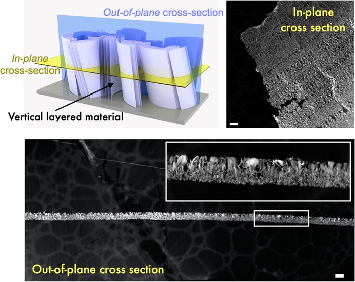
Layered materials (LMs) such as graphene or MoS2 have attracted a great deal of interest recently. These materials offer unique functionalities due to their structural anisotropy characterized by weak van der Waals bonds along the out-of-plane axis and covalent bonds in the in-plane direction. A central requirement to access the structural information on complex nanostructures built upon LMs is to control the relative orientation of each sample prior to their inspection, e.g., with transmission electron microscopy (TEM). However, developing sample preparation methods that result in large inspection areas and ensure full control over the sample orientation while avoiding damage during the transfer to the TEM grid is challenging. Here, we demonstrate the feasibility of deploying ultramicrotomy for the preparation of LM samples in TEM analyses. We show how ultramicrotomy leads to the reproducible large-scale production of both in-plane and out-of-plane cross sections, with bulk vertically oriented MoS2 and WS2 nanosheets as a proof of concept. The robustness of the prepared samples is subsequently verified by their characterization by means of both high-resolution TEM and Raman spectroscopy measurements. Our approach is fully general and should find applications for a wide range of materials as well as of techniques beyond TEM, thus paving the way to the systematic large-area mass-production of cross-sectional specimens for structural and compositional studies.
Keywords: electron microscopy, sample preparation, in- and out-of-plane cross sections, ultramicrotomy, layered materials, transmission electron microscopy characterization, Raman spectroscopy
Introduction
Recent developments in electron microscopy are one of the main drivers of the tremendous recent progress that the field of material science is experiencing. Thanks to this progress, it is now possible to provide extensive information on structural1 and chemical2 properties of materials down to the single-atom scale. A family of materials that have attracted a great deal of interest are layered materials3 (LMs) such as graphene or MoS2. In the context of the fabrication of nanostructures built upon LMs, one of the main requirements to achieve tailored geometries is being able to control the orientation of the prepared sample for their characterization, e.g., being able to image them using transmission electron microscopy (TEM) measurements and complementary techniques.
However, the preparation of samples of LMs in a manner that is suitable for their flexible inspection by means of TEM is challenging, since one needs to achieve full control over the transfer and relative orientation of these nanostructures from the substrate onto the TEM grid. For in-plane inspection, one of the most popular approaches is the direct exfoliation of LM nanosheets from their bulk form via either mechanical or liquid methods,4−8 which allows verifying their crystalline structure and chemical composition.9−11 However, exfoliation limits the available inspection area since in general the totality of material cannot be transferred. In the case of out-of-plane cross sections, these are usually prepared using focus ion beam (FIB),12−18 which again often results in small inspection areas.
Here, we adopt a popular preparation method used for biological samples,19,20 ultramicrotomy, and demonstrate its feasibility for the preparation of LM samples for their subsequent TEM characterization. Ultramicrotomy is being increasingly adopted as an attractive and complementary option for producing the high-quality TEM specimens,21,22 and it can also be used to tailor the dimensions of the fabricated cross sections.23−26
In this work we demonstrate the significant potential that ultramicrotomy has for the sample preparation and TEM inspection of layered materials. Our strategy achieves the reproducible large-scale production of both in-plane and out-of-plane cross-section samples of LMs, with MoS2 and WS2 as a proof of concept. We demonstrate how this strategy makes possible the high-resolution TEM imaging in both in the in- and out-of-plane direction. Our method is also suitable to prepare LM samples for their inspection with other techniques, as we demonstrate here by carrying out Raman spectroscopy characterization of the same cross sections.
Results and Discussion
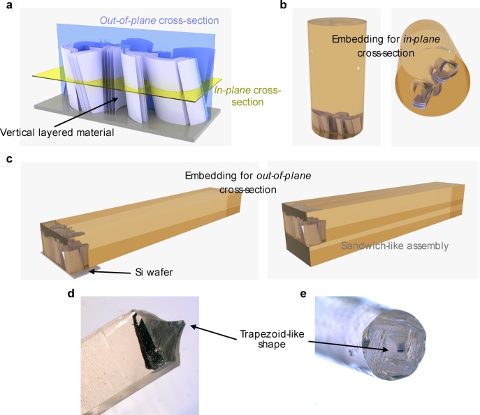
Bulk vertical MoS2 and WS2 nanosheets grown on top of a SiO2/Si substrate have been used for fabricating in-plane (with MoS2) and out-of-plane (with WS2) cross sections, as indicated in Figure 1a. Figure 1b,c summarizes the procedures followed to create these in-plane and out-of-plane cross sections, respectively. The two approaches differ in the orientation of the specimens within the epoxy block, which is the main factor that needs to be considered before sectioning. In the case of the in-plane cross sections, the specimen is kept in one side of the cured epoxy block, as shown in Figure 1b. If our goal instead is to access the out-of-plane direction, the specimen is embedded into epoxy creating a sandwich-like assembly with the specimen in the middle of it (see Figure 1c). In this way, the out-of-plane direction can be aligned parallel to the knife edge used for the sectioning. In order to facilitate the access along both directions, two different embedding containers have been used, as indicated in Figures S1 and S2 from the Supporting Information (SI).
Figure 1.
(a) Schematic representation of vertically oriented layered materials grown on top of a substrate, where we indicate the directions corresponding to the in- and out-of-plane cross sections. (b, c) Illustrations representing the specimen embedded in the cured epoxy block for in- and out-of-plane configurations, respectively. (d, e) Optical microscope images of the trimmed top of the epoxy block for out-of-plane and in-plane configurations, respectively.
Embedding of MoS2 for In-Plane Cross Sections
The embedding and curing procedures for the in-plane cross-section sample preparation are straightforward since the whole process takes place at once. The wafer was mounted on top of a cylindrical Teflon mold (see Figure S1a). After filling the hole with the prepared epoxy, the epoxy/wafer system was cured for 9 h.
Embedding of WS2 for Out-of-Plane Cross Sections
In this particular case, a flat silicone rubber mold was used (Figure S2a). We began by filling half of the silicone rubber mold with the prepared epoxy. The wafer containing the specimen was placed on top of the epoxy, with the specimen side facing the epoxy, as illustrated in the left panel of Figure 1c. The whole epoxy/wafer system was then placed inside a furnace and cured at a temperature of 70 °C for 4 h. This is the minimum time required in order to make sure that the specimen can be fully detached from the silicon wafer, resulting in an epoxy/specimen system. This system was then again placed inside the silicon rubber mold, covered with epoxy, and cured for 12 h. Figure 1c (right) shows a schematic representation of the final sandwich-like assembly. Notice that for these out-of-plane samples one needs to establish an appropriate curing time for the two parts of the sandwich. This is important in order to ensure uniform thicknesses during sectioning. In addition, long curing times can efficiently prevent charging effects and contamination during the TEM inspection.
Preparing the Epoxy/Specimen Blocks for Sectioning
Before sectioning, it is necessary to trim down the epoxy/specimen system such that its dimensions become much smaller than the length of the knife. To achieve this, we manually trimmed the side of the epoxy block containing the specimen, using both a razor blade and a scalpel. The trimmed area was reduced down to a small trapezoid-like shape with a length of around 0.5 mm, as shown in Figure 1d,e. At the end of this procedure, the epoxy–specimen system is ready for being sectioned. For further details of the embedding, trimming, and sectioning procedures, see the SI.
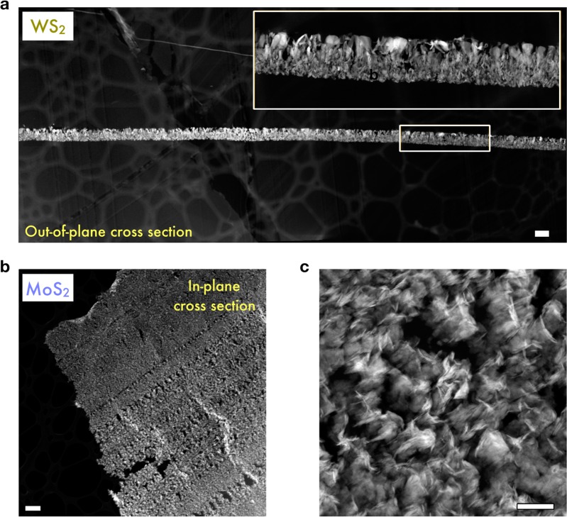
To assess the stability of the cross sections fabricated using the ultramicrotomy method, TEM measurements were carried out. Figure 2 displays the low-magnification high-angle annular dark field (HAADF) scanning transmission electron microscopy (STEM) images from representative areas of the out-of-plane cross sections of WS2 (Figure 2a) and in-plane cross sections of MoS2 (Figure 2b,c). From these low-magnification images, one can clearly appreciate the large cross-section areas that have been produced with our procedure for both the in-plane and the out-of-plane orientations. Remarkably, the achievable lengths of the fabricated out-of-plane cross sections turn out to be up to several tens of microns (for a maximum length of around 35 μm). Moreover, the real advantage of the ultramicrotomy method is that these 35 μm cross sections are contained within a single slice, and in one TEM grid it is possible to fit up to ten of these slices. This implies that the effective cross-section length available for TEM inspection is much larger, up to 350 μm, representing an improvement by more than a factor of 20 as compared to the FIB results. Similar considerations apply to the in-plane MoS2 cross sections (which cannot be produced using FIB), where we achieve large effective areas suitable for TEM inspection of up to 250 μm2 or even larger, depending on the density of the specimen on top of the wafer.
Figure 2.
(a, b) Low-magnification HAADF-STEM images of the out-of-plane WS2 and in-plane MoS2 cross sections, respectively. The inset in part a displays the magnification of the rectangular area marked by a white box. (c) Magnified area from part b. The scale bars in parts a and b correspond to 1 μm, and that in part c corresponds to 200 nm.
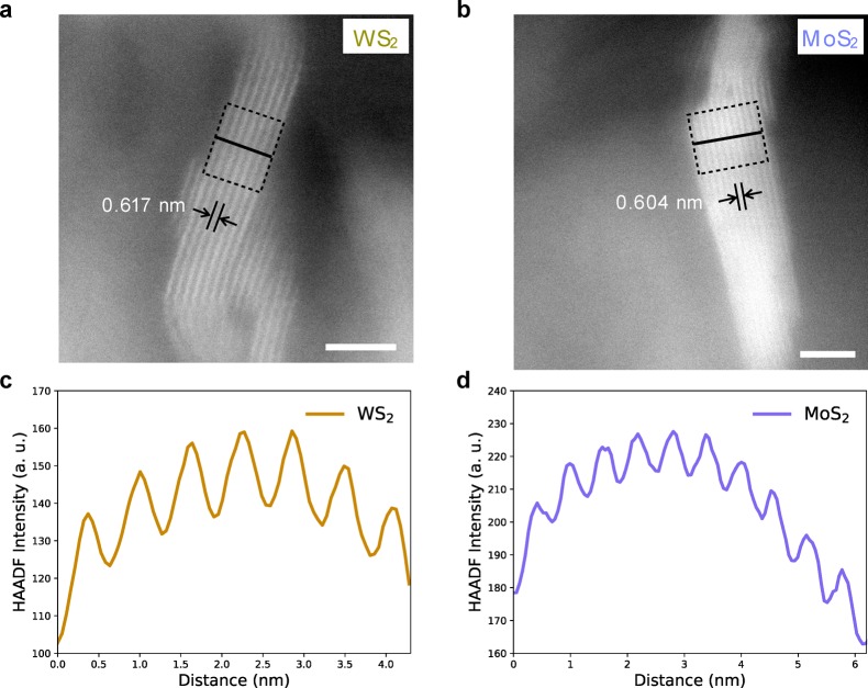
Figure 3a,b displays HAADF-STEM images of representative regions of the same out-of-plane WS2 and in-plane MoS2 cross-sectional specimens studied in Figure 2. In both cases we can resolve vertical lattice fringes. From the spacing between maxima determined from the intensity profiles integrated over a rectangular area (see Figure 3c,d), we are able to measure the distance between these fringes. Our results indicate that the spacings between lattice fringes are 0.604 ± 0.025 nm for MoS2 and 0.617 ± 0.025 nm for WS2. These results are consistent with the (002) d-spacing within 2H-MoS2 and 2H-WS2 crystals.27,28
Figure 3.
(a, b) HAADF-STEM images of vertically aligned WS2 layers and MoS2 layers, respectively, where the scale bars are 5 nm. (c, d) The associated lattice parameters are determined from the spacing between maxima of the intensity profiles in parts a and b averaged over the indicated rectangular areas.
A crucial advantage of our approach is that it is also suitable to prepare cross-section samples of layered materials for their inspection with other techniques complementary to TEM. We have exploited this feature by carrying out room-temperature Raman spectroscopy measurements of the same WS2 and MoS2 cross-section samples discussed above. For these measurements we used an excitation laser with a wavelength of 514 nm, keeping the laser power under 0.5 mW at all times.
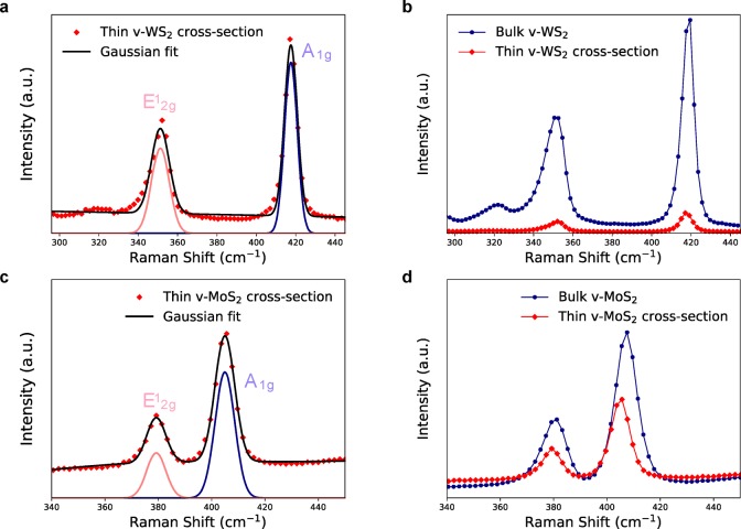
Figure 4a displays the Raman spectrum corresponding to the out-of-plane WS2 cross-section. As one can observe, this Raman spectrum is dominated by the first-order modes, indicated by the in-plane E12g peak at 349.7 cm–1 and the out-of-plane A1g peak at 417.5 cm–1. This analysis highlights how the intensity of the out-of-plane peak (A1g) is markedly higher than that of its in-plane counterpart (E12g). Our findings are consistent with previous reports in the literature and further confirm the vertical orientation of the WS2 nanosheets.29−32
Figure 4.
(a, c) Raman spectra obtained from the out-of-plane WS2 and in the in-plane MoS2 cross sections, respectively. A Gaussian fit of the E12g and A1g peaks is also displayed. (b, d) Comparison between the Raman spectra of the out-of-plane WS2 and the in-plane MoS2 cross sections with the ones obtained from the corresponding bulk vertical WS2 specimen.
Furthermore, by comparing the Raman spectra of the out-of-plane WS2 cross-section with the one obtained from the corresponding bulk specimen (Figure 4b) one finds that the positions of the in-plane (out-of-plane) peak shift toward smaller (larger) frequencies by 0.7 cm–1 (0.9 cm–1). It is worth noting that the Raman spectrum of the bulk vertical WS2 specimen was collected using the same excitation laser wavelength but with a higher laser power instead, 5 mW. For this reason, the intensity of the bulk spectrum increases significantly as compared to the cross-section case.
It has been reported that the peak shifts of both the out-of-plane A1g and in-plane E12g modes are related to the specimen thickness variations. For instance, when comparing regular exfoliated WS2 with its bulk counterpart, one of the most relevant effects is the blue-shift of the A1g mode and red-shift of the E12g one when increasing the number of layers.33 This behavior appears to be at odds with the expectations from a classical model for coupled harmonic oscillators, where both modes are predicted to blue-shift.34 However, the same behavior that we observed in WS2 has also been reported in other members of the TMD family.35,36 Several mechanisms have been ascribed to explain this anomalous shift of the E12g peak, including the presence of additional interlayer interactions,37−39 stacking induced structural changes,40 and long-range Coulombic interlayer interactions.37 While further studies are needed, additional interlayer interactions are likely to play a role in our case due to the structural disorder of the vertical WS2 (arising from the growth dynamics itself) illustrated in Figure 2a.
Moving to the Raman spectrum obtained from the in-plane MoS2 cross-section sample, we find that it exhibits two main peaks located at 379.2 and 405.0 cm–1, respectively (see Figure 4c). These two peaks arise from the Raman modes associated with the in-plane vibration of molybdenum and sulfur atoms (E12g) and the out-of-plane vibration of sulfur atoms (A1g). The ratio of the intensity between the two peaks, A1g/ E12g, turns out to be around 3, providing further confirmation of the vertical configuration of the MoS2 nanosheets.
With a similar motivation, we compare the Raman spectra corresponding to the in-plane MoS2 cross-section sample with its bulk counterpart (see Figure 4d). From this comparison, we find that the peaks associated with the out-of-plane A1g and the in-plane E12g modes shift toward larger frequencies by 2.2 and 0.9 cm–1, respectively. Therefore, the frequency shift of the A1g peak is more pronounced than that of the E12g one. This feature has also been reported in MoS2,40 where it is ascribed to the structural diversity induced by the synthesis of the specimens.
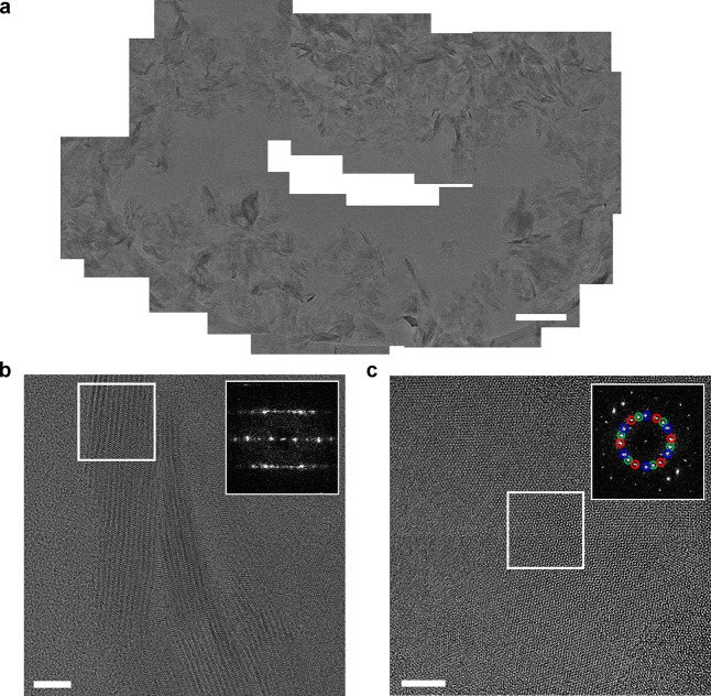
These local structure variations inferred from Raman spectroscopy can be further confirmed by TEM measurements. Figure 5 displays a reconstruction composed by low-magnification bright-field TEM images taken from the in-plane MoS2 cross-section sample. We can observe that the relative orientation of the MoS2 nanosheets is not homogeneous: some of them are vertically oriented as expected, but others turn out to be perpendicular to the former. This property is verified by the corresponding high-resolution TEM (HRTEM) images. As illustrated in Figure 5b, we can find vertically aligned nanosheets, which exhibit a hexagonal crystal system structure corresponding to the 2H-MoS2 polytype. Moreover, we can also find Moiré regions arising from the superposition of different 2H-MoS2 nanosheets oriented along the [001] direction and rotated with respect to each other. In Figure 5c we display the HRTEM image of a Moiré region in MoS2, where the FFT in the inset illustrates the overlap of three MoS2 nanosheets along the [001] direction with different relative angles.
Figure 5.
(a) Low-magnification TEM image of a MoS2 patch aligned in the in-plane direction. (b) HRTEM image of vertically aligned MoS2 nanosheets along the [112̅0] direction with its corresponding FFT calculated in the area marked by a white square as the inset. (c) HRTEM image of a Moiré region in MoS2, where the FFT in the inset and displays the overlap of three MoS2 nanosheets along the [001] direction. The scale bar in part a corresponds to 200 nm; those in parts b and d correspond to 5 nm.
Conclusions
In this work, we have presented and validated a strategy based on ultramicrotomy for the efficient and reproducible fabrication of large-area in-plane and out-of-plane cross sections of layered materials, with MoS2 and WS2 as a proof of concept. This approach, which bypasses some of the limitations that affect other cross-section sample preparation techniques, allows one to reliably manipulate and control the relative orientation of the prepared samples for their characterization without affecting or damaging the specimen in any way.
We have verified the structural robustness of the resulting cross-section specimens by means of detailed characterization studies using both transmission electron microscopy and Raman spectroscopy measurements. Remarkably, the structural insights provided from the TEM and the Raman data confirm each other’s findings and demonstrate that our ultramicrotomy-based approach can be reliably adopted for the systematic structural characterization of in-plane and out-of-plane LM specimens.
While in this work we have demonstrated the viability of the ultramicrotomy-based cross-section sample preparation approach for the case of MoS2 and WS2, the method is fully general and should find applications enabling novel structural studies for several other layered materials, including, for example, topological insulator materials. As such, we believe that the method proposed here should represent an important contribution to the ongoing efforts of the nanotechnology community, paving the way for the systematic large-area mass-fabrication of cross-sectional specimens for advancing the structural and compositional inspection in a wide range of materials.
Experimental Section
Layered Material Synthesis
As a proof of concept of our proposed microtomy-based strategy for sample preparation, we have carried out the sectioning of two different LMs, namely, bulk MoS2 and WS2 vertical nanosheets. These were synthesized using a two-step process, where a 700 nm thick Mo (186 nm thick W) layer was first sputtered onto a SiO2/Si substrate and subsequently sulfurized at 700 °C (750 °C) into MoS2 (WS2). The sulfurization process was carried out in a gradient tube furnace from Carbolite Gero. The sample was placed in the middle zone and gradually heated to 700 °C (750 °C) at a rate of 10 °C/min. Once the sample reached the desired temperature, 400 mg of sulfur was heated to 220 °C. The sulfur was placed upstream from the sample. Note that argon gas was used as a carrier gas.
In the following, we present the details of the three main steps required for the sectioning procedure: embedding into epoxy, trimming, and finally sectioning using ultramicrotomy.
Embedding into Epoxy
All the specimens were embedded in Agar low-viscosity resin, from Agar Scientific. The ratio between the hardeners (VH1 and VH2) and the curing temperature was optimized to achieve the desired hardness, while the two other components of the recipe, the low viscosity resin and the accelerator, were kept fixed at values of 48 g and 2.5 g. For further details, see Table S1 of the Supporting Information (SI).
Ultramicrotomy
The trimming and sectioning have been carried out using an RMC Ultramicrotome PowerTome PC from Boeckeler Instruments. For the trimming of the cured epoxy block containing the specimen, a razor blade and a sculpt were applied. For the sectioning procedure, we employed a DiATOME diamond knife with a cutting angle of 35° and a clearance angle at 6°. The cutting speed and the sectioning thickness were generally set to 1 mm/s and a programmed thickness of 20 or 30 nm, respectively. The ribbons of the slices were directly collected from the deionizer bath and deposited onto a 300-mesh lacey carbon film copper TEM grid. The ribbons have been dried using a filter paper when deposited onto the TEM grid.
Characterization Techniques
Transmission electron microscopy (TEM) measurements were carried out in a Titan Cube microscope using an acceleration voltage of 300 kV. Its spatial resolution at Scherzer defocus conditions is 0.08 nm in the high-resolution transmission electron microscopy (HRTEM) mode, while the resolution is around 0.19 nm in the HAADF-STEM (high-angle annular dark field–scanning transmission electron microscopy) mode.
Raman Spectroscopy
The Raman spectroscopy measurements were carried out using a Renishaw Invia Reflex microscope. A 514 nm incident laser beam was used in a backscattering configuration. The signal was analyzed with a 1800 l/mm grating, resulting in a spectral resolution of around 1 cm–1.
Acknowledgments
M.O.C. acknowledges support from The Netherlands Organizational for Scientific Research (NWO) through the Nanofront program. M.B., S.E.v.H., and S.C.-B. acknowledge financial support from ERC through the Starting Grant “TESLA” Grant Agreement 805021.
Supporting Information Available
The Supporting Information is available free of charge at https://pubs.acs.org/doi/10.1021/acsami.9b22586.
Further details about the embedding, trimming, and sectioning procedures, as well as on the HRTEM analysis and interpretation (PDF)
Author Contributions
M.B. and S.E.v.H. synthesized the vertical MoS2 and WS2 samples, respectively. M.O.C. performed the Ultramicrotomy and the TEM measurements. M.O.C. analyzed the TEM data. M.B. and S.E.v.H. performed and analyzed the Raman measurements. M.O.C., M.B., S.E.v.H., and S.C.-B. prepared the figures and the discussion of the results. S.C.-B. designed and supervised the experiments. All the authors contributed to the writing of the manuscript.
The authors declare no competing financial interest.
Supplementary Material
References
- Enyashin A. N.; Bar-Sadan M.; Houben L.; Seifert G. Line Defects in Molybdenum Disulfide Layers. J. Phys. Chem. C 2013, 117, 10842–10848. 10.1021/jp403976d. [DOI] [Google Scholar]
- Zamani R. R.; Hage F. S.; Lehmann S.; Ramasse Q. M.; Dick K. A. Atomic Resolution Spectrum Imaging of Semiconductor Nanowires. Nano Lett. 2018, 18, 1557–1563. 10.1021/acs.nanolett.7b03929. [DOI] [PubMed] [Google Scholar]
- Novoselov K. S.; Jiang D.; Schedin F.; Booth T. J.; Khotkevich V. V.; Morozov S. V.; Geim A. K. Two-Dimensional Atomic Crystals. Proc. Natl. Acad. Sci. U. S. A. 2005, 102, 10451–10453. 10.1073/pnas.0502848102. [DOI] [PMC free article] [PubMed] [Google Scholar]
- Ottaviano L.; Palleschi S.; Perrozzi F.; D’Olimpio G.; Priante F.; Donarelli M.; Benassi P.; Nardone M.; Gonchigsuren M.; Gombosuren M.; Lucia A.; Moccia G.; Cacioppo O. A. Mechanical Exfoliation and Layer Number Identification of MoS2 Revisited. 2D Mater. 2017, 4, 045013. 10.1088/2053-1583/aa8764. [DOI] [Google Scholar]
- Ma H.; Shen Z.; Ben S. Understanding the Exfoliation and Dispersion of MoS2 Nanosheets in Pure Water. J. Colloid Interface Sci. 2018, 517, 204–212. 10.1016/j.jcis.2017.11.013. [DOI] [PubMed] [Google Scholar]
- Splendiani A.; Sun L.; Zhang Y.; Li T.; Kim J.; Chim C.-Y.; Galli G.; Wang F. Emerging Photoluminescence in Monolayer MoS2. Nano Lett. 2010, 10, 1271–1275. 10.1021/nl903868w. [DOI] [PubMed] [Google Scholar]
- Brorson M.; Carlsson A.; Topsøe H. The Morphology of MoS2, WS2, Co-Mo-S, Ni-Mo-S and Ni-W-S Nanoclusters in Hydrodesulfurization Catalysts Revealed by HAADF-STEM. Catal. Today 2007, 123, 31–36. 10.1016/j.cattod.2007.01.073. [DOI] [Google Scholar]
- Deokar G.; Vancsó P.; Arenal R.; Ravaux F.; Casanova-Cháfer J.; Llobet E.; Makarova A.; Vyalikh D.; Struzzi C.; Lambin P.; Jouiad M.; Colomer J.-F. MoS2-Carbon Nanotube Hybrid Material Growth and Gas Sensing. Adv. Mater. Interfaces 2017, 4, 1700801. 10.1002/admi.201700801. [DOI] [Google Scholar]
- Eda G.; Yamaguchi H.; Voiry D.; Fujita T.; Chen M.; Chowalla M. Correction to Photoluminescence from Chemically Exfoliated MoS2. Nano Lett. 2012, 12, 526–526. 10.1021/nl2044887. [DOI] [PubMed] [Google Scholar]
- Tinoco M.; Maduro L.; Masaki M.; Okunishi E.; Conesa-Boj S. Strain-Dependent Edge Structures in MoS2 Layers. Nano Lett. 2017, 17, 7021–7026. 10.1021/acs.nanolett.7b03627. [DOI] [PMC free article] [PubMed] [Google Scholar]
- Fang S.; Wen Y.; Allen C. S.; Ophus C.; Han G. G. D.; Kirkland A. I.; Kaxiras E.; Warner J. H. Atomic Electrostatic Maps of 1D Channels in 2D Semiconductors using 4D Scanning Transmission Electron Microscopy. Nat. Commun. 2019, 10, 1–9. 10.1038/s41467-019-08904-9. [DOI] [PMC free article] [PubMed] [Google Scholar]
- Wang D.; Wang Y.; Chen X.; Zhu Y.; Zhan K.; Cheng H.; Wang X. Layer-by-Layer Thinning of Two-Dimensional MoS2 Films by Using a Focused Ion Beam. Nanoscale 2016, 8, 4107–4112. 10.1039/C5NR05768J. [DOI] [PubMed] [Google Scholar]
- Tinoco M.; Maduro L.; Conesa-Boj S. Metallic Edge States in Zig-Zag Vertically-Oriented MoS2 Nanowalls. Sci. Rep. 2019, 9, 1–7. 10.1038/s41598-019-52119-3. [DOI] [PMC free article] [PubMed] [Google Scholar]
- Deokar G.; Rajput N. S.; Vancsó P.; Ravaux F.; Jouiad M.; Vignaud D.; Cecchet F.; Colomer J.-F. Large Area Growth of Vertically Aligned Luminescent MoS2 Nanosheets. Nanoscale 2017, 9 (1), 277–287. 10.1039/C6NR07965B. [DOI] [PubMed] [Google Scholar]
- Bolhuis M.; Hernandez-Rueda J.; van Heijst S. E.; Rivas M. T.; Kuipers L.; Conesa-Boj S.. Vertically-Oriented MoS2 Nanosheets for Nonlinear Optical Devices. 2020, arXiv:2001.10513. arXiv.org e-Print archive. https://arxiv.org/abs/2001.10513. [DOI] [PubMed]
- Cho S.-Y.; Kim S. J.; Lee Y.; Kim J.-S.; Jung W.-B.; Yoo H.-W.; Kim J.; Jung H.-T. Highly Enhanced Gas Adsorption Properties in Vertically Aligned MoS2 Layers. ACS Nano 2015, 9, 9314–9321. 10.1021/acsnano.5b04504. [DOI] [PubMed] [Google Scholar]
- Kong D.; Wang H.; Cha J. J.; Pasta M.; Koski K. J.; Yao J.; Cui Y. Synthesis of MoS2 and MoSe2 Films with Vertically Aligned Layers. Nano Lett. 2013, 13, 1341–1347. 10.1021/nl400258t. [DOI] [PubMed] [Google Scholar]
- Li H.; Wu H.; Yuan S.; Qian H. Synthesis and Characterization of Vertically Standing MoS2 Nanosheets. Sci. Rep. 2016, 6, 1–9. 10.1038/srep21171. [DOI] [PMC free article] [PubMed] [Google Scholar]
- Dubochet J.; Adrian M.; Chang J.-J.; Homo J.-C.; Lepault J.; McDowall A. W.; Schultz P. Cryo-Electron Microscopy of Vitrified Specimens. Q. Rev. Biophys. 1988, 21, 129–228. 10.1017/S0033583500004297. [DOI] [PubMed] [Google Scholar]
- Murphy A. P.; McNeil G. Precision Ultramicrotome of Simplified Design. Rev. Sci. Instrum. 1964, 35, 132–134. 10.1063/1.1718695. [DOI] [Google Scholar]
- Wei L.-Y.; Li T. Ultramicrotomy of Powder Material for TEM/STEM Study. Microsc. Res. Tech. 1997, 36, 380–381. . [DOI] [PubMed] [Google Scholar]
- Bae J.; Cichocka M. O.; Zhang Y.; Bacsik Z.; Bals S.; Zou X.; Willhammar T.; Hong S. B. Phase Transformation Behavior of a Two-Dimensional Zeolite. Angew. Chem., Int. Ed. 2019, 58, 10230–10235. 10.1002/anie.201904825. [DOI] [PubMed] [Google Scholar]
- Xu Q.; Rioux R. M.; Whitesides G. M. Fabrication of Complex Metallic Nanostructures by Nanoskiving. ACS Nano 2007, 1, 215–227. 10.1021/nn700172c. [DOI] [PubMed] [Google Scholar]
- Lipomi D. J.; Kats M. A.; Kim P.; Kang S. H.; Aizenberg J.; Capasso F.; Whitesides G. M. Fabrication and Replication of Arrays of Single- or Multicomponent Nanostructures by Replica Molding and Mechanical Sectioning. ACS Nano 2010, 4, 4017–4026. 10.1021/nn100993t. [DOI] [PubMed] [Google Scholar]
- Lipomi D. J.; Martinez R. V.; Kats M. A.; Kang S. H.; Kim P.; Aizenberg J.; Capasso F.; Whitesides G. M. Patterning the Tips of Optical Fibers with Metallic Nanostructures Using Nanoskiving. Nano Lett. 2011, 11, 632–636. 10.1021/nl103730g. [DOI] [PubMed] [Google Scholar]
- Lipomi D. J.; Martinez R. V.; Whitesides G. M. Use of Thin Sectioning (Nanoskiving) to Fabricate Nanostructures for Electronic and Optical Applications. Angew. Chem., Int. Ed. 2011, 50, 8566–8583. 10.1002/anie.201101024. [DOI] [PubMed] [Google Scholar]
- Sojkova M.; Vegso K.; Mrkyvkova N.; Hagara J.; Hutar P.; Rosova A.; Caplovicova M.; Ludacka U.; Skakalova V.; Majkova E.; Siffalovic P.; Hulman M. Tuning the Orientation of Few-Layers MoS2 Films Using One-Zone Sulfurization. RSC Adv. 2019, 9, 29645. 10.1039/C9RA06770A. [DOI] [PMC free article] [PubMed] [Google Scholar]
- Liu Z.; Murphy A. W. A.; Kuppe C.; Hooper D. C.; Valev V. K.; Ilie A. WS2 Nanotubes, 2D Nanomeshes, and 2D In-Plane Films Thorugh One Single Chemical Vapor Deposition Route. ACS Nano 2019, 13, 3896. 10.1021/acsnano.8b06515. [DOI] [PMC free article] [PubMed] [Google Scholar]
- Sharma S.; Bhagat S.; Singh J.; Singh R. C.; Sharma S. Excitation-Dependent Photoluminescence from WS2 Nanostructures Synthesized Via Top-Down Approach. J. Mater. Sci. 2017, 52, 11326–11336. 10.1007/s10853-017-1303-3. [DOI] [Google Scholar]
- Eftekhari A. Tungsten Dichalcogenides (WS2, WSe2, and WTe2) Materials Chemistry and Applications. J. Mater. Chem. A 2017, 5, 18299. 10.1039/C7TA04268J. [DOI] [Google Scholar]
- Wang X. H.; Zheng C. C.; Ning J. Q. Influence of Curvature Strain and Van der Waals Force on the Inter-layer Vibration Mode of WS2 Nanotubes: A Confocal Micro-Raman Spectroscopy Study. Sci. Rep. 2016, 6, 33091. 10.1038/srep33091. [DOI] [PMC free article] [PubMed] [Google Scholar]
- Kim H.-S.; Patel M.; Kim J.; Jeong M. S. Growth of Wafer-Scale Standing Layers of WS2 for Self-Biased High-Speed UV-Visible-NIR Optoelectronic Devices. ACS Appl. Mater. Interfaces 2018, 10, 3964–3974. 10.1021/acsami.7b16397. [DOI] [PubMed] [Google Scholar]
- Zhao W.; Ghorannevis Z.; Amara K. K.; Pang J. R.; Toh M.; Zhang X.; Kloc C.; Tane P. H.; Eda G. Lattice Dynamics in Mono- and Few-Layer Sheets of WS2 and WSe2. Nanoscale 2013, 5, 9677. 10.1039/c3nr03052k. [DOI] [PubMed] [Google Scholar]
- Li T.; Galli G. Electronic Properties of MoS2 Nanoparticles. J. Phys. Chem. C 2007, 111, 16192–16196. 10.1021/jp075424v. [DOI] [Google Scholar]
- Ataca C.; Topsakal M.; Akturk E.; Ciraci S. A Comparative Study of Lattice Dynamics of Three- and Two- Dimensional MoS2. J. Phys. Chem. C 2011, 115, 16354. 10.1021/jp205116x. [DOI] [Google Scholar]
- Lee C.; Yan H.; Brus L. E.; Heinz T. F.; Hone J.; Ryu S. Anomalous Lattice Vibrations of Single and Few-Layer MoS2. ACS Nano 2010, 4, 2695–2700. 10.1021/nn1003937. [DOI] [PubMed] [Google Scholar]
- Wieting T. J.; Verble J. L. Interlayer Bonding and the Lattice Vibrations of -GaSe. Phys. Rev. B 1972, 5, 1473–1479. 10.1103/PhysRevB.5.1473. [DOI] [Google Scholar]
- Ghosh P. N.; Maiti C. R. Interlayer Force and Davydov Splitting in 2H-MoS2. Phys. Rev. B: Condens. Matter Mater. Phys. 1983, 28, 2237–2239. 10.1103/PhysRevB.28.2237. [DOI] [Google Scholar]
- Ghosh P. N. Davydov Splitting and Multipole Interactions. Solid State Commun. 1976, 19, 639–642. 10.1016/0038-1098(76)91093-0. [DOI] [Google Scholar]
- Yan J.; Xia J.; Wang X.; Liu L.; Kuo J.-L.; Tay B. K.; Chen S.; Zhou W.; Liu Z.; Shen Z. X. Stacking-Dependent Interlayer Coupling in Trilayer MoS2 with Broken Inversion Symmetry. Nano Lett. 2015, 15, 8155–8161. 10.1021/acs.nanolett.5b03597. [DOI] [PubMed] [Google Scholar]
Associated Data
This section collects any data citations, data availability statements, or supplementary materials included in this article.


