Abstract
In this paper, we demonstrate a tunable periodic hourglass-shaped graphene arrays absorber in the infrared (IR) and terahertz (THz) frequency bands. The effects of graphene geometric parameters, chemical potentials, periods, and incident angles on the pure absorption characteristics are studied by using the Finite Difference Time Domain (FDTD) method. In addition, this paper also analyzes the pure absorption characteristics of bilayer graphene arrays. The simulation results show that the maximum absorption reaches 38.2% for the monolayer graphene structure. Furthermore, comparing the bilayer graphene structure with the monolayer structure under the same conditions shows that the bilayer structure has a tunable dual-band selective absorption effect and has a higher maximum absorption of 41.7%. Moreover, it was found that there are dual-band tunable absorption peaks at and with the maximum absorption of 41.7% and 11%. The proposed structure is a convenient method which could be used in the design of graphene-based optoelectronic devices, biosensors, and environmental monitors.
Keywords: graphene, metamaterial absorber, surface plasmon resonance, finite difference time domain
1. Introduction
Graphene is a two-dimensional (2D) carbon nanomaterial with a hexagonal honeycomb structure composed of carbon atoms and sp2 hybrid orbitals [1,2]. Owing to its unique optoelectronic properties, graphene is one of the most promising optoelectronic materials and is widely used in the field of batteries, materials processing, biomolecular sensing, food safety, and communications [3,4,5,6,7,8,9,10,11,12,13,14,15,16,17]. Additionally, graphene also play an essential role in metadevices, such as detectors and modulators [18,19,20]. Taking the modulator as an example, the application of graphene enables the modulation depth of the modulator to reach 100%.
In the infrared (IR) and terahertz (THz) range, when graphene interacts with incident light [21,22,23,24,25,26,27,28], surface plasmon polaritons (SPPs) and localized surface plasmons (LSPs) occur. SPPs are surface waves that are excited at the boundary of the material; the excitation of these charge waves is achieved by properly matching the free space and surface plasmon momenta of the system. On the other hand, LSPs are subwavelength surface waves supported in materials whose characteristic dimensions are comparable to the excitation wavelength [29,30]. It is the latter that contributes to the absorption mechanism, and leads to the enhancement of absorption [31,32,33,34,35]. The migration of graphene electrons is described by the interband and intraband contributions, which are affected by the external electric fields and magnetic fields. The electromagnetic properties of graphene can be easily tuned by applying external electric fields, magnetic fields, or by chemical doping [36,37]. All of these can make the properties of graphene better than metal [38]. The use of graphene localized surface plasmon characteristics can effectively control the absorption and transmission of light, making graphene attractive to researchers.
In the past few years, graphene-based absorbers (GBA) have received much attention. In 2015, Ke et al. reported a cross-shaped graphene array absorber that achieved 20% absorption [39]; Xiao et al. proposed periodic graphene ring arrays and introduced a good angular polarization tolerance that achieved an absorption of 25% [40]; Fang et al. reached 30% absorption by incorporating graphene nanodisk arrays into an active device [41]. Although the maximum absorption of monolayer graphene has been greatly improved compared with its predecessors, the maximum absorption of a pure graphene layer is not more than 30%. Therefore, designing a graphene absorber with a higher absorption is an urgent problem to be solved. We compared our work with [42], which achieves ultrabroadband and nearly 100% perfect absorption by etching a cross-shaped structure on doped silicon. However, the substrate and patterned metamaterial of our proposed structure are different from those of [42], and for this reason, the absorption rate of our proposed structure rarely exceeds 50% [43]. When compared with [40,41], our structure has the following advantages: the structure has more geometric structures that can be optimized, so that we have more options to adjust its absorption characteristics; the structure is easy to integrate and the substrate of this structure is silicon and silica.
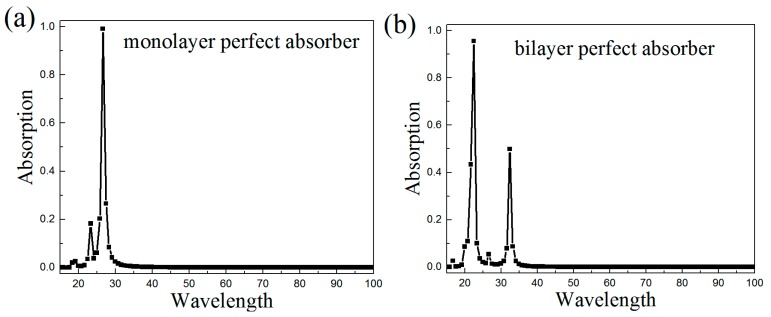
On the basis of these points, this paper proposed a GBA which is composed of periodically patterned “hourglass” graphene metamaterial arrays, and the proposed structure can reach an absorption of 41.7%. For a symmetric dielectric environment, the predicted maximum absorption does not exceed 50% [43], so the maximum absorption of 41.7% in this structure is still a remarkably good result. If a layer of golden mirror is added to the bottom of the structure, our proposed structure can also realize perfect absorption (Perfect Absorption in the Appendix A, shown in Figure A1).
The hourglass-shaped structure consists of two isosceles triangles and two semi-ellipses. These two triangles are symmetrical and intersect with each other. The reason why this structure was chosen are as follows: (1) the two symmetrical and intersecting triangles can realize zero-energy states; (2) the semi-ellipses have two geometric parameters that can be tuned, we can adjust more geometric parameters to adjust its absorption characteristics; (3) the two triangles and two semi-ellipses consist of a continuous graphene structure. In the second section, the hourglass-shaped structure is presented, we also introduce the calculation methods of the absorption spectra. In the third section, we study the influence of different parameters on the absorption characteristics. Then, we analyze the effects of bilayer graphene on absorption. Finally, we summarize the whole project.
2. Geometric Structures and Methods
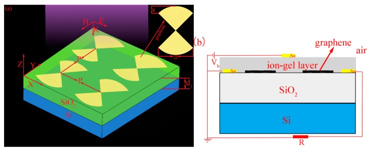
The schematic of the tunable hourglass-shaped GBA is shown in Figure 1a. The period of the cell structure along the X and Y directions is P. There are two semi-ellipses and the semimajor and semiminor axis of the semi-ellipse are L and R. The middle part of the graphene structure is composed of two symmetrical isosceles triangles that intersect at the vertices. The graphene arrays are attached to a silicon (Si) substrate separated by a thin silica (SiO2) spacer layer with a thickness of . In this paper, the absorption spectra and the localized electric field distribution of the structure are studied using the Finite Difference Time Domain (FDTD) method [44]. The antisymmetric, symmetric, and perfectly matched layer (PML) boundary conditions are used in the X, Y, and Z directions, respectively. The isosceles triangle of this structure has two sides of length . The semimajor (L) and semiminor (R) axis of the ellipse are both (that is the special case of an ellipse: circle). The thickness of SiO2 () and Si are and infinity. The period (P) of the structure is . The thickness of monolayer graphene is . The uniform mesh accuracy along the X and Y directions are adopted as 20 nm, and the Z direction is 1 nm. The relative permittivity of Si and SiO2 are adopted as 1.96 and 3.9 [45,46]. The entire system is illuminated by a plane wave propagating along the negative Z direction with total electric field E polarizing along the X direction. The position of the electric field monitor is placed at the same position of the graphene layer and is larger than the graphene layer boundary.
Figure 1.
(a) The schematic of “hourglass” graphene arrays structure with period (P), semimajor axis (L), semiminor axis (R). The two layers of substrate structure are Si and SiO2. The thickness of SiO2 is . (b) The side view of the structure which manipulates the chemical potential () of graphene by applying a voltage ().
The chemical potential () can be dynamically tuned by changing the value of total carrier density () that can be expressed as follows [47,48,49,50,51]:
| (1) |
where and are the reduced Planck’s constant and the Fermi velocity [52]. The total carrier density () can be changed by applying a voltage (), so can be expressed as
| (2) |
where and are the permittivity of free space and the dielectric layer, and e are the thickness of the SiO2 layer and charge of an electron, respectively. Therefore Equation (1) can be expressed as follows:
| (3) |
It can be seen from Equation (3) that with other parameters are fixed, and is related to . When a is employed between the top and back gates (as shown in Figure 1b; the ion-gel layer is the conductive layer), and can be dynamically tuned. We can change by applying a specific , then the change of leads to the change of , and we can obtain a specific value of .
The conductivity of monolayer graphene can be calculated with the random phase approximation (RPA) in the local limit, consisting of intraband and interband contributions [53,54,55], which can be expressed as follows:
| (4) |
| (5) |
| (6) |
where is the Boltzmann constant, is the angular frequency of the electromagnetic wave, T is temperature and is fixed at 300 K, is the Drude relaxation time with the carrier mobility and Fermi velocity . In the THz region and below, where the photon energy , the interband part (Equation (6)) can be neglected compared to the intraband. Therefore, can be described by the Drude-like model [56], then Equation (5) can be written as
| (7) |
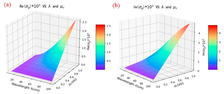
When , the real and imaginary parts of as functions of the chemical potential () and the wavelength () are displayed in Figure 2a,b. As can be seen from Figure 2, both Re () and Im () can be dynamically tuned by changing and , because the amplitude modulation and the spectral shift of the resonance are determined by the real and imaginary parts of , respectively.
Figure 2.
The real (a) and imaginary part (b) of as functions of and .
For continuous monolayer graphene, the transmission and reflection are expressed as follows [39,57]:
| (8) |
| (9) |
where is the wave impedance of air; the absorption can be expressed as
| (10) |
In the range of visible light, is almost a constant, resulting in only 2.3% absorption. varies with the change of in the range of terahertz and far infrared. At , , the absorption is 3.9%, while when , the absorption is 0.8%, which is significantly lower than that of patterned graphene. For a symmetric dielectric environment, the predicted maximum absorption would not exceed 50% [43]. The absorption may approach the maximum predicted value when graphene is formed into a specific pattern and/or by adjusting its geometric parameters or the dielectric environment.
3. Simulation Results and Discussions
3.1. The Influence of Different Chemical Potentials on Absorption
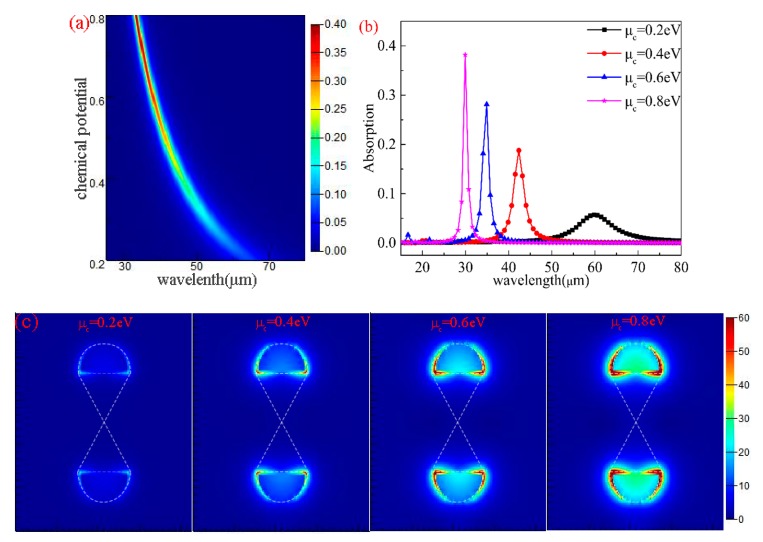
Different from other materials, graphene can be dynamically tunable when its geometry is fixed. This dynamic tenability is achieved by changing . From Equation (7), can mainly determine , and can be tuned and controlled by using an electrostatic field or chemical doping. According to Equation (3), can reach specific values by applying specific . By fixing the structure parameters at (L = 0.4 μm, R = 0.4 μm, p = 0.3 μm), the absorption characteristics of different values are simulated under vertical plane wave illumination. As shown in Figure 3a, when we change from 0.2 to 0.8 eV, the maximum absorption increases simultaneously, and experiences blue shift. Then, we picked 0.2, 0.4, 0.6, 0.8 eV, and analyzed the absorption spectra. As shown in Figure 3b, the maximum absorption increases and reached 38.2% with absorption spectrum blue shift. Meanwhile, the working bandwidth narrowed gradually with the increase in . Compared with the monolayer unpatterned graphene with an absorption of only 2.3% [58], the maximum absorption improved greatly. We demonstrate the physical mechanism as follows: (1) according to Equation (1), the higher leads to a higher value of , the higher value of contributed to the increase in plasmonic oscillation, and the increase in plasmonic oscillation leads to the enhancement of the maximum absorption; (2) the working bandwidth mainly depends on how fast and change with frequency , where and n are both constants. For the gradually changing conductivity of continuous graphene film, the fastest changes are related to . It can be seen from Figure 3a that with the increase in , the resonance wavelength () of the corresponding absorption peak gradually decreases. Because and are inversely proportional, gradually increases with the decrease in ; and since the cotangent function is a monotonously decreasing function, the working bandwidth gradually narrows as increases.
Figure 3.
(a) The graph of the graphene absorption. (b) The absorption spectra corresponding to the chemical potential from 0.2 to 0.8 eV. (c) The corresponding electric field intensity distribution under different values.
Figure 3c shows the local electric field distribution at maximum absorption resonance wavelengths for different values. As increases, the intensity of electric field distribution also increases continuously, as well as only being distributed at the edge of the two semi-ellipses; the triangle has no distribution. This is because the two triangles are symmetrical and intersect with each other, thus realizing zero-energy states, and the triangular connection does not play any role in the excitation of plasmons [59]. In addition, the LSPs are enhanced with the increase in ; this kind of enhancement leads to a stronger electric field and a higher absorption.
3.2. The Influence of Different Semiminor Axes on Absorption
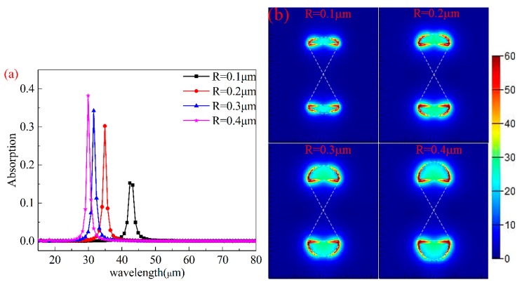
In this paper, the relationships between the elliptical semiminor axis (R) and absorption spectra of the structure were also studied. Keeping other parameters unchanged (), R was changed from to with an interval of . The results are shown in Figure 4a. With an increase in R, the resonance wavelength moves from to with a significant blue shift. Simultaneously, the maximum absorption increases from 15.2% to 38.2%, a strong enhancement on graphene absorption.
Figure 4.
(a) The graph of the graphene absorption corresponding to the semiminor axis from to . (b) The corresponding electric field intensity distribution under different R values.
Figure 4b shows the local electric field distribution at maximum absorption resonance wavelengths for different R values. The electric field is distributed on both sides of the semi-elliptical arc, and the intensity of electric field is basically unchanged with the increase in R. However, with the increase in R, the effective area of graphene increases; the increase in the effective area can make graphene gather more energy, leading to the enhancement in the maximum absorption. The localized surface plasmon resonance (LSPR) on both sides of the semi-elliptical arc is the main contribution to the wavelength position of the spectra; so with the increase in R, the resonance wavelength experiences blue shift. Then, we can conclude that with the increase in R, the maximum absorption increases and is accompanied by blue shift.
3.3. The Influence of Different Semimajor Axes of the Ellipse on Absorption
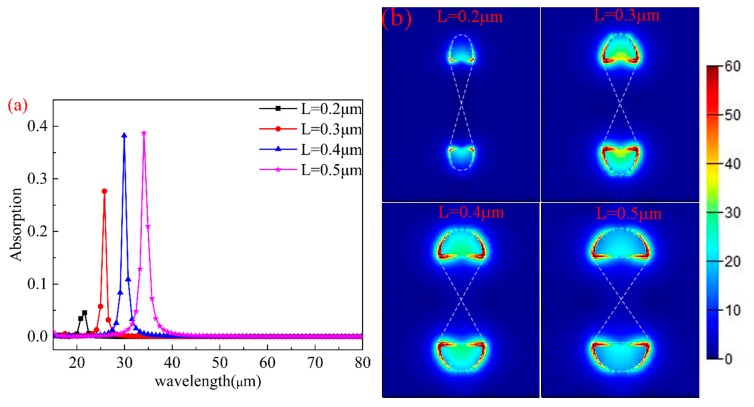
This paper analyzes the influence of different semimajor axes (L) of the ellipse on absorption characteristics. While keeping other parameters unchanged (), L of the ellipse was changed. Figure 5a plots the absorption spectra of different L values from to with an interval of . As described in the figure, the resonance wavelengths have strong red shifts and the maximum absorption gradually increases. The resonance wavelength shifts from to , while the maximum absorption increases from 4.5% to 38.7% and increased nearly 9 times. The increase in the absorption is a result of the graphene surface plasmon resonance (SPR) gradually increasing with the increase in L.
Figure 5.
(a) The absorption spectra of the structure with different L values. (b) The electric field distributions at the maximum absorption for .
The distribution of the electric field intensity at maximum absorptions for different L values are shown in Figure 5b. The electric field intensity is only distributed at the edge of the two semi-ellipses. This phenomenon is mainly caused by the accumulation of electric charge. When L increases, the distance between adjacent graphene arrays decreases, which leads to the enhancement of coupling between neighboring graphene arrays, and the increase in coupling results in the red shifts and the increase in absorption. Figure 5b also shows that local enhancement of the electromagnetic field can be realized, which is caused by the strong electric dipole resonance excited by the charge at both ends of L. This strong resonance can effectively capture the energy of light and have enough time to eliminate the loss of graphene.
3.4. The Influence of Different Periods on Absorption
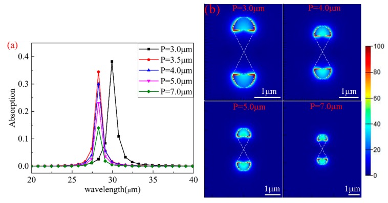
The absorption spectra for different periods (P) are plotted in Figure 6a. As can been seen from the figure, P has a significant impact on the maximum absorption but less on the wavelength, when other parameters remain unchanged ( ). As P increases, the resonance wavelength first decreases and then is maintained at ; simultaneously, the maximum absorption gradually decreases. The physical mechanisms are explained as follows: (1) with the increases in P, the resonance wavelengths are almost unchanged because the resonance condition remains unchanged [39]; (2) the resonance wavelength first decreases at low P due to the coupling of neighboring graphene; (3) the filling factor of graphene decreases, leading to the decrease in absorption (the filling factor is defined as the ratio of the graphene resonator to the entire resonant unit cell).
Figure 6.
(a) The absorption spectra of the structure with different P values. (b) The electric field distributions at the absorption peak for .
The distribution of the electric field intensity at maximum absorptions with different P values are shown in Figure 6b. The electric field is mainly distributed on both sides and the bottom of the semi-ellipse. As can be seen from Figure 6b, as P increases, the electric field intensity concentrated on the ellipse becomes stronger. However, because the filling factor of graphene gradually decreases, and the effect of electric field intensity on the absorption is smaller than that of graphene filling factor on the absorption, the absorption gradually decreases with the increase in P.
3.5. The Influence of Different Incident Angles on Absorption
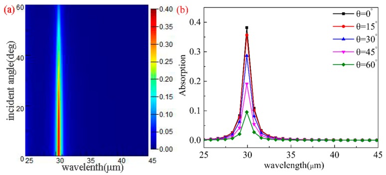
We also studied the influence of different incident angles () on the absorption characteristics of the structure with the other parameters unchanged (). Figure 7a,b demonstrate the resonance wavelength under different values. As can be seen from the figure, the maximum absorption peaks are sensitive to different values and the value decreases with the increase in . However, the resonance wavelengths are insensitive to different values. The maximum absorption is obtained under the condition of so-called critical coupling or rate equipartition [60]. In the case of oblique incident, the condition of critical coupling cannot be achieved. Furthermore, because P is much smaller than the incident wavelength, the resonance frequency is almost independent of the incident angle , so the phase difference of the light field at the adjacent graphene structures are basically independent of [43]. Figure 7c reveals the corresponding electric field intensity distribution at the resonance wavelength with different incident angles. It can be seen from the figure that as increases, the electric field strength decreases continuously and is mainly distributed on both sides of the ellipse.
Figure 7.
(a,b) The absorption spectra of the structure with different θ values. (c) The electric field distributions at the absorption peak for .
4. Bilayer Graphene Arrays
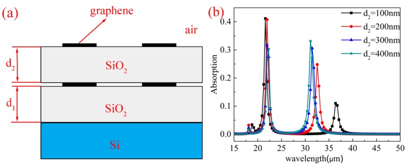
We also analyzed the influence of bilayer graphene arrays on absorption characteristics. The results show that the maximum absorption can be further improved using the bilayer graphene arrays. As depicted in Figure 8a, the structure consisting of two-layer graphene arrays are separated by a thin SiO2 layer with a thickness of . Whilst keeping other parameters unchanged (), the absorption spectra of various values from 100 to 400 nm with 100 nm intervals are illustrates in Figure 8b. When is fixed at , it can be seen form the spectra that there are dual-band absorption peaks at and with an absorption efficiency 41.7% and 11%, respectively. Moreover, when , the maximum absorption at the short-band can reach 41.7%, which exceeds that of the monolayer graphene arrays with the same parameters (38.2%). The shifts of the resonance wavelength are different for the two bands. For the long-band and short-band, the resonance wavelength undergoes blue shift and slight red shift, respectively. As for the maximum absorption, the maximum absorption at the short-band decreases with the increase in , but for the long-band, the maximum absorption increases with the increase in . According to our simulation results, the upper layer of the graphene structure mainly contributes to the short-band, and the lower layer mainly contributes to the long-band. Therefore, the bilayer graphene structure allows us to adjust the two absorption peaks and their bandwidths separately to achieve different absorption characteristics.
Figure 8.
(a) The side view of the structure consisting of bilayer graphene arrays covered with two thin SiO2 layers with thickness and . (b) The absorption spectra of the structure with different values.
5. Conclusions
In this paper, we analyze the tunable absorption enhancement of periodic hourglass-shaped GBA. By increasing R and L of the ellipse, the absorption can be further enhanced. With the increase in R and L, the absorption experiences red shifts and blue shifts, respectively. The variation of P and are sensitive to maximum absorption intensity, but insensitive to the resonance wavelength. This paper also presents the absorption characteristics of bilayer graphene, which can bring about higher absorption (41.7%) and even can make dual-band absorption occur. We hope that our work can provide a potential application in graphene-based optoelectronic devices, biosensors, and environmental monitoring.
Appendix A
Figure A1.
(a) The monolayer perfect absorption of this structure, (b) The bilayer perfect absorption of this structure.
Author Contributions
Conceptualization, Y.Q. and Y.Z.; methodology, Y.Z.; software, Y.Z.; validation, D.Y.; formal analysis, T.Z.; investigation, B.Z.; resources, L.W.; data curation, Y.Z. and C.L.; writing—original draft preparation, Y.Z.; writing—review and editing, Y.Z.; visualization, C.L.; supervision, Y.Q. and X.D.; project administration, Y.Q.; funding acquisition, Y.Q. and X.W.; English editing and grammar checking, Y.Y.; All authors have read and agreed to the published version of the manuscript.
Funding
This study is supported by the National Natural Science Foundation of China, grant numbers 61367005 and 61865008, the Natural Science Foundation of Gansu Province, China, grant numbers 17JR5RA078, and Northwest Normal University Young Teachers’ Scientific Research Capability Upgrading Program, grant numbers NWNU-LKQN-17-6.
Conflicts of Interest
The authors declare no conflict of interest.
References
- 1.Novoselov K.S., Geim A.K., Morozov S.V., Jiang D., Zhang Y., Dubonos S.V., Firsov A.A. Electric field effect in atomically thin carbon films. Science. 2004;306:666–669. doi: 10.1126/science.1102896. [DOI] [PubMed] [Google Scholar]
- 2.Novoselov K.S., Geim A.K., Morozov S., Jiang D., Katsnelson M.I., Grigorieva I., Firsov A.A. Two-dimensional gas of massless Dirac fermions in graphene. Nature. 2005;438:197. doi: 10.1038/nature04233. [DOI] [PubMed] [Google Scholar]
- 3.Yoo E., Kim J., Hosono E., Zhou H.S., Kudo T., Honma I. Large reversible Li storage of graphene nanosheet families for use in rechargeable lithium ion batteries. Nano Lett. 2008;8:2277–2282. doi: 10.1021/nl800957b. [DOI] [PubMed] [Google Scholar]
- 4.Rodrigo D., Limaj O., Janner D., Etezadi D., De Abajo F.J.G., Pruneri V., Altug H. Mid-infrared plasmonic biosensing with graphene. Science. 2015;349:165–168. doi: 10.1126/science.aab2051. [DOI] [PubMed] [Google Scholar]
- 5.Mueller T., Xia F., Avouris P. Graphene photodetectors for high-speed optical communications. Nat. Potonics. 2010;4:297. doi: 10.1038/nphoton.2010.40. [DOI] [Google Scholar]
- 6.Wang G., Liu J., Tang S., Li H., Cao D. Cobalt oxide–graphene nanocomposite as anode materials for lithium-ion batteries. J. Solid State Electr. 2011;15:2587–2592. doi: 10.1007/s10008-010-1254-y. [DOI] [Google Scholar]
- 7.Liu G., Liu Y., Tang L., Liu X., Fu G., Liu Z. Semiconductor-enhanced Raman scattering sensors via quasi-three-dimensional Au/Si/Au structures. Nanophotonics. 2019;8:1095–1107. doi: 10.1515/nanoph-2019-0078. [DOI] [Google Scholar]
- 8.Fowler J.D., Allen M.J., Tung V.C., Yang Y., Kaner R.B., Weiller B.H. Practical chemical sensors from chemically derived graphene. ACS Nano. 2009;3:301–306. doi: 10.1021/nn800593m. [DOI] [PubMed] [Google Scholar]
- 9.Schall D., Neumaier D., Mohsin M., Chmielak B., Bolten J., Porschatis C., Templ W. 50 GBit/s photodetectors based on wafer-scale graphene for integrated silicon photonic communication systems. ACS Photonics. 2014;1:781–784. doi: 10.1021/ph5001605. [DOI] [Google Scholar]
- 10.He X. Tunable terahertz graphene metamaterials. Carbon. 2015;82:229–237. doi: 10.1016/j.carbon.2014.10.066. [DOI] [Google Scholar]
- 11.Qin F., Chen Z., Chen X., Yi Z., Yao W., Duan T., Wu P., Yang H., Li G., Yi Y. A Tunable Triple-Band Near-Infrared Metamaterial Absorber Based on Au Nano-Cuboids Array. Nanomaterials. 2020;10:207. doi: 10.3390/nano10020207. [DOI] [PMC free article] [PubMed] [Google Scholar]
- 12.Cen C., Chen Z., Xu D., Jiang L., Chen X., Yi Z., Yi Y. High Quality Factor, High Sensitivity Metamaterial Graphene—Perfect Absorber Based on Critical Coupling Theory and Impedance Matching. Nanomaterials. 2020;10:95. doi: 10.3390/nano10010095. [DOI] [PMC free article] [PubMed] [Google Scholar]
- 13.Low T., Avouris P. Graphene plasmonics for terahertz to mid-infrared applications. ACS Nano. 2014;8:1086–1101. doi: 10.1021/nn406627u. [DOI] [PubMed] [Google Scholar]
- 14.Chen J., Fan W., Zhang T., Tang C., Chen X., Wu J., Yu Y. Engineering the magnetic plasmon resonances of metamaterials for high-quality sensing. Opt. Express. 2017;25:3675–3681. doi: 10.1364/OE.25.003675. [DOI] [PubMed] [Google Scholar]
- 15.Ha N.R., Jung I.P., La I.J., Jung H.S., Yoon M.Y. Ultra-sensitive detection of kanamycin for food safety using a reduced graphene oxide-based fluorescent aptasensor. Sci. Rep. 2017;7:40305. doi: 10.1038/srep40305. [DOI] [PMC free article] [PubMed] [Google Scholar]
- 16.Ameri S.K., Kim M., Kuang I.A., Perera W.K., Alshiekh M., Jeong H., Lu N. Imperceptible electrooculography graphene sensor system for human–robot interface. NPJ 2D Mater. Appl. 2018;2:19. doi: 10.1038/s41699-018-0064-4. [DOI] [Google Scholar]
- 17.Piper J.R., Fan S. Total absorption in a graphene monolayer in the optical regime by critical coupling with a photonic crystal guided resonance. Acs Photonics. 2014;1:347–353. doi: 10.1021/ph400090p. [DOI] [Google Scholar]
- 18.Vicarelli L., Vitiello M.S., Coquillat D., Lombardo A., Ferrari A.C., Knap W., Tredicucci A. Graphene field-effect transistors as room-temperature terahertz detectors. Nat. Mater. 2012;11:865–871. doi: 10.1038/nmat3417. [DOI] [PubMed] [Google Scholar]
- 19.Vhmadivand A., Gerislioglu B., Ramezani Z. Gated graphene island-enabled tunable charge transfer plasmon terahertz metamodulator. Nanoscale. 2019;11:8091–8095. doi: 10.1039/C8NR10151E. [DOI] [PubMed] [Google Scholar]
- 20.Liang G., Hu X., Yu X., Shen Y., Li L.H., Davies A.G., Wang Q.J. Integrated terahertz graphene modulator with 100% modulation depth. ACS Photonics. 2015;2:1559–1566. doi: 10.1021/acsphotonics.5b00317. [DOI] [Google Scholar]
- 21.Xiao T.H., Gan L., Zhi Y. Graphene surface plasmon polaritons transport on curved substrates. Photonics Res. 2015;3:300–307. doi: 10.1364/PRJ.3.000300. [DOI] [Google Scholar]
- 22.Lu H., Zeng C., Zhang Q., Liu X., Hossain M.M., Reineck P., Gu M. Graphene-based active slow surface plasmon polaritons. Sci. Rep. 2015;5:8443. doi: 10.1038/srep08443. [DOI] [PMC free article] [PubMed] [Google Scholar]
- 23.Tredicucci A., Vitiello M.S. Device concepts for graphene-based terahertz photonics. IEEE J. Sel. Top. Quant. 2013;20:130–138. doi: 10.1109/JSTQE.2013.2271692. [DOI] [Google Scholar]
- 24.Dubinov A.A., Aleshkin V.Y., Mitin V., Otsuji T., Ryzhii V. Terahertz surface plasmons in optically pumped graphene structures. J. Phys. Condens. Matter. 2011;23:145302. doi: 10.1088/0953-8984/23/14/145302. [DOI] [PubMed] [Google Scholar]
- 25.Bai T., Lv L., Du W., Fang W., Wang Y. Improving the Tribological and Anticorrosion Performance of Waterborne Polyurethane Coating by the Synergistic Effect between Modified Graphene Oxide and Polytetrafluoroethylene. Nanomaterials. 2020;10:137. doi: 10.3390/nano10010137. [DOI] [PMC free article] [PubMed] [Google Scholar]
- 26.de Ceglia D., Vincenti M.A., Grande M., Bianco G.V., Bruno G., D’Orazio A., Scalora M. Tuning infrared guided-mode resonances with graphene. JOSA B. 2016;33:426–433. doi: 10.1364/JOSAB.33.000426. [DOI] [Google Scholar]
- 27.Wang Y., Chen Z., Xu D., Yi Z., Chen X., Chen J., Tang Y., Wu P., Li G., Yi Y. Triple-band perfect metamaterial absorber with good operating angle polarization tolerance based on split ring arrays. Results Phys. 2020;16:102951. doi: 10.1016/j.rinp.2020.102951. [DOI] [Google Scholar]
- 28.Gubin M.Y., Leksin A.Y., Shesterikov A.V., Prokhorov A.V., Volkov V.S. All-Plasmonic Switching Effect in the Graphene Nanostructures Containing Quantum Emitters. Nanomaterials. 2020;10:122. doi: 10.3390/nano10010122. [DOI] [PMC free article] [PubMed] [Google Scholar]
- 29.Nikitin A.Y., Guinea F., García-Vidal F.J., Martín-Moreno L. Edge and waveguide terahertz surface plasmon modes in graphene microribbons. Phys. Rev. B. 2011;84:161407. doi: 10.1103/PhysRevB.84.161407. [DOI] [Google Scholar]
- 30.Yakubovsky D.I., Stebunov Y.V., Kirtaev R.V., Voronin K.V., Voronov A.A., Arsenin A.V., Volkov V.S. Graphene-supported thin metal films for nanophotonics and optoelectronics. Nanomaterials. 2018;8:1058. doi: 10.3390/nano8121058. [DOI] [PMC free article] [PubMed] [Google Scholar]
- 31.Liu Y., Cheng R., Liao L., Zhou H., Bai J., Liu G., Duan X. Plasmon resonance enhanced multicolour photodetection by graphene. Nat. Commun. 2011;2:579. doi: 10.1038/ncomms1589. [DOI] [PMC free article] [PubMed] [Google Scholar]
- 32.Xiong F., Zhang J., Zhu Z., Yuan X., Qin S. Ultrabroadband, more than one order absorption enhancement in graphene with plasmonic light trapping. Sci. Rep. 2015;5:16998. doi: 10.1038/srep16998. [DOI] [PMC free article] [PubMed] [Google Scholar]
- 33.Huang H., Ke S., Wang B., Long H., Wang K., Lu P. Numerical study on plasmonic absorption enhancement by a rippled graphene sheet. J. Lightwave Technol. 2016;35:320–324. doi: 10.1109/JLT.2016.2636846. [DOI] [Google Scholar]
- 34.Sun H., Ling L., Ren Z., Memon S.A., Xing F. Effect of Graphene Oxide/Graphene Hybrid on Mechanical Properties of Cement Mortar and Mechanism Investigation. Nanomaterials. 2020;10:113. doi: 10.3390/nano10010113. [DOI] [PMC free article] [PubMed] [Google Scholar]
- 35.Zhou Q., Liu P., Bian L.A., Liu H., Liu C., Chen G. Controlling enhanced absorption in graphene metamaterial. Opt. Commun. 2018;413:310–316. doi: 10.1016/j.optcom.2017.12.078. [DOI] [Google Scholar]
- 36.Xin L., Hai-Long W., Hui P., Huai-Zhe X. Gap opening and tuning in single-layer graphene with combined electric and magnetic field modulation. Chinese Phys. B. 2011;20:047302. [Google Scholar]
- 37.Grande M., Bianco G.V., Perna F.M., Capriati V., Capezzuto P., Scalora M., D’Orazio A. Reconfigurable and optically transparent microwave absorbers based on deep eutectic solvent-gated graphene. Sci. Rep. 2019;9:1–9. doi: 10.1038/s41598-019-41806-w. [DOI] [PMC free article] [PubMed] [Google Scholar]
- 38.Grigorenko A.N., Polini M., Novoselov K.S. Graphene plasmonics. Nat. Photonics. 2012;6:749. doi: 10.1038/nphoton.2012.262. [DOI] [Google Scholar]
- 39.Ke S., Wang B., Huang H., Long H., Wang K., Lu P. Plasmonic absorption enhancement in periodic cross-shaped graphene arrays. Opt. Express. 2015;23:8888–8900. doi: 10.1364/OE.23.008888. [DOI] [PubMed] [Google Scholar]
- 40.Xiao S., Wang T., Liu Y., Xu C., Han X., Yan X. Tunable light trapping and absorption enhancement with graphene ring arrays. Phys. Chem. Chem. Phys. 2016;18:26661–26669. doi: 10.1039/C6CP03731C. [DOI] [PubMed] [Google Scholar]
- 41.Fang Z., Wang Y., Schlather A.E., Liu Z., Ajayan P.M., García de Abajo F.J., Halas N.J. Active tunable absorption enhancement with graphene nanodisk arrays. Nano Lett. 2013;14:299–304. doi: 10.1021/nl404042h. [DOI] [PubMed] [Google Scholar]
- 42.Cheng Y.Z., Withayachumnankul W., Upadhyay A., Headland D., Nie Y., Gong R.Z., Abbott D. Ultrabroadband plasmonic absorber for terahertz waves. Adv. Opt. Mater. 2015;3:376–380. [Google Scholar]
- 43.Thongrattanasiri S., Koppens F.H., De Abajo F.J.G. Complete optical absorption in periodically patterned graphene. Phys. Rev. Lett. 2012;108:047401. doi: 10.1103/PhysRevLett.108.047401. [DOI] [PubMed] [Google Scholar]
- 44.Chen P.Y., Alu A. Atomically thin surface cloak using graphene monolayers. ACS Nano. 2011;5:5855–5863. doi: 10.1021/nn201622e. [DOI] [PubMed] [Google Scholar]
- 45.Kane Y. Numerical solution of initial boundary value problems involving Maxwell’s equations in isotropic media. IEEE T. Antenn. Propag. 1966;14:302–307. doi: 10.1109/TAP.1966.1138693. [DOI] [Google Scholar]
- 46.Lin G.R., Chang Y.C., Liu E.S., Kuo H.C., Lin H.S. Low refractive index Si nanopillars on Si substrate. Appl. Phys. Lett. 2007;90:181923. doi: 10.1063/1.2736281. [DOI] [Google Scholar]
- 47.Andryieuski A., Lavrinenko A.V. Graphene metamaterials based tunable terahertz absorber: Effective surface conductivity approach. Opt. Express. 2013;21:9144–9155. doi: 10.1364/OE.21.009144. [DOI] [PubMed] [Google Scholar]
- 48.Gusynin V.P., Sharapov S.G., Carbotte J.P. Magneto-optical conductivity in Graphene. J. Phys. Condens. Matter. 2007;19:026222. doi: 10.1088/0953-8984/19/2/026222. [DOI] [Google Scholar]
- 49.Li Z.Q., Henriksen E.A., Jiang Z., Hao Z., Martin M.C., Kim P., Basov D.N. Dirac charge dynamics in graphene by infrared spectroscopy. Nat. Phys. 2008;4:532. doi: 10.1038/nphys989. [DOI] [Google Scholar]
- 50.Vakil A., Engheta N. Transformation optics using graphene. Science. 2011;332:1291–1294. doi: 10.1126/science.1202691. [DOI] [PubMed] [Google Scholar]
- 51.Gao W., Shu J., Qiu C., Xu Q. Excitation of plasmonic waves in graphene by guided-mode resonances. ACS Nano. 2012;6:7806–7813. doi: 10.1021/nn301888e. [DOI] [PubMed] [Google Scholar]
- 52.Lee S.H., Choi M., Kim T.T., Lee S., Liu M., Yin X., Zhang X. Switching terahertz waves with gate-controlled active graphene metamaterials. Nat. Mater. 2012;11:936. doi: 10.1038/nmat3433. [DOI] [PubMed] [Google Scholar]
- 53.Jablan M., Buljan H., Soljačić M. Plasmonics in graphene at infrared frequencies. Phys. Rev. B. 2009;80:245435. doi: 10.1103/PhysRevB.80.245435. [DOI] [Google Scholar]
- 54.Hwang E.H., Sarma S.D. Dielectric function, screening, and plasmons in two-dimensional graphene. Phys. Rev. B. 2007;75:205418. doi: 10.1103/PhysRevB.75.205418. [DOI] [Google Scholar]
- 55.Qi Y., Zhang Y., Liu C., Zhang T., Zhang B., Wang L., Wang X. A tunable terahertz metamaterial absorber composed of elliptical ring graphene arrays with refractive index sensing application. Results Phys. 2020:103012. doi: 10.1016/j.rinp.2020.103012. [DOI] [Google Scholar]
- 56.Fallahi A., Perruisseau-Carrier J. Design of tunable biperiodic graphene metasurfaces. Phys. Rev. B. 2012;86:195408. doi: 10.1103/PhysRevB.86.195408. [DOI] [Google Scholar]
- 57.Grande M., Bianco G.V., Vincenti M.A., de Ceglia D., Capezzuto P., Scalora M., Bruno G. Optically transparent microwave polarizer based on quasi-metallic graphene. Sci. Rep. 2015;5:17083. doi: 10.1038/srep17083. [DOI] [PMC free article] [PubMed] [Google Scholar]
- 58.Mak K.F., Sfeir M.Y., Wu Y., Lui C.H., Misewich J.A., Heinz T.F. Measurement of the optical conductivity of graphene. Phys. Rev. Lett. 2008;101:196405. doi: 10.1103/PhysRevLett.101.196405. [DOI] [PubMed] [Google Scholar]
- 59.Potasz P., Güçlü A.D., Hawrylak P. Zero-energy states in triangular and trapezoidal graphene structures. Phys. Rev. B. 2010;81:033403. doi: 10.1103/PhysRevB.81.033403. [DOI] [Google Scholar]
- 60.Teperik T.V., De Abajo F.G., Borisov A.G., Abdelsalam M., Bartlett P.N., Sugawara Y., Baumberg J.J. Omnidirectional absorption in nanostructured metal surfaces. Nat. Photonics. 2008;2:299. doi: 10.1038/nphoton.2008.76. [DOI] [Google Scholar]


