

Mixed-conducting particulate composite can form functional electronic components by varying particle size and density.
Abstract
Bioelectronic devices should optimally merge a soft, biocompatible tissue interface with capacity for local, advanced signal processing. Here, we introduce an organic mixed-conducting particulate composite material (MCP) that can form functional electronic components by varying particle size and density. We created MCP-based high-performance anisotropic films, independently addressable transistors, resistors, and diodes that are pattern free, scalable, and biocompatible. MCP enabled facile and effective electronic bonding between soft and rigid electronics, permitting recording of neurophysiological data at the resolution of individual neurons from freely moving rodents and from the surface of the human brain through a small opening in the skull. We also noninvasively acquired high–spatiotemporal resolution electrophysiological signals by directly interfacing MCP with human skin. MCP provides a single-material solution to facilitate development of bioelectronic devices that can safely acquire, transmit, and process complex biological signals.
INTRODUCTION
Soft and biocompatible materials constitute an effective solution for interfacing electronic devices with biological tissue (1, 2). A wide variety of organic materials are inherently flexible, chemically inert, nontoxic, and have tunable physical properties, making them optimal for this function (3, 4). In addition, conducting and semiconducting organics can form nonlinear electronic components (such as transistors and diodes) capable of biological signal sensing and transduction (5–7). Bioelectronic devices often require advanced signal processing to implement diagnostic and therapeutic operations, from differential amplification and time division multiplexing to analog to digital conversion and high-speed digital communication (2). Silicon-based electronics can accomplish each of these functions, with a large repository of preexisting designs, fabrication processes, and experiential knowledge (8). These technologies are rigid and incompatible with ion-rich physiologic environments (9, 10). A device with organic material at the abiotic/biotic interface to perform signal preprocessing and advanced silicon-based circuits for subsequent signal communication and analysis would combine the beneficial properties of both approaches. However, two substantial challenges hinder realization of these devices: (i) lack of stable, high-performance, independently addressable organic components for integrated circuits, and (ii) absence of scalable, biocompatible processes to seamlessly integrate soft, organic materials with rigid silicon-based circuits. Because conducting polymers are mixed (ionic and electronic) conductors (11, 12), they offer the possibility of ion-based modulation of electronic charge carriers within a single material, in contrast to inorganics, where multiple different materials need to be precisely combined to accomplish these operations.
Here, we introduce an innovative, soft, biocompatible composite material (MCP) composed of mixed-conducting polymer particles and an electronically insulating, ion-conducting scaffolding polymer matrix. It can be used to create different electronic components based on the size and density of its constituent particles. The physical processes to generate MCP are scalable, solvent free and preserve the electrical properties of the conducting polymer. We determined that MCP can form functional anisotropic films, independently addressable transistors, resistors, and diodes. MCP permits anisotropic, high–spatiotemporal resolution sensing and transmission and enabled recording of high-quality neurophysiological data from the surface of the human brain. We also used MCP to directly interface with human skin and were able to noninvasively sense spatially localized nerve action potentials from a small surface area. Therefore, MCP can form multiple different electronic components, with potential applicability to enhancing safety and efficacy of a wide range of bioelectronic devices.
RESULTS
We hypothesized that, by manipulating the sparsity and size of mixed-conducting particles within a scaffolding polymer matrix that has controllable ionic conductivity, we could create films with various regimes of electronic operation (Fig. 1A). This approach would allow a single material to function as multiple different principle electronic components, eliminating the need for several bonded layers of patterned conducting, semiconducting, and insulating materials. The key properties of the mixed-conducting particles are their mean diameter (α) and density (ρ) in solution, which interact to determine the longest electrically conducting length that the particles can form (mean free path, λ). The relationship of these parameters with the distance between electrical terminals in both the horizontal (d1 and d2) and vertical plane (h) results in five major functional modes of operation:
Fig. 1. Control of size and density of mixed-conducting particles in an ion conducting scaffolding matrix enables various regimes of electronic operation.
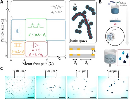
(A) MCP operates as an anisotropic conducting film (orange), transistor (blue), transistor with independent gating (green), diode (red), or resistor (black) depending on the particle size (α) and mean free path (λ) within the material (as represented by the schematic, upper right). These properties are defined with respect to distance between horizontally adjacent (and, for the anisotropic film, corresponding vertical) electrodes (lower right). The gray rectangles represent substrate and the yellow rectangles represent the electrical terminals. (B) Physical process steps to create conducting polymer particles: A solution of conducting polymer PEDOT:PSS with solvent additives is prepared (top). The solution is evaporated to form a highly conducting film. The film is broken into large particles and crushed into microparticles using a ball mill. The size of microparticles is reduced via sonication (bottom). Scale bar, 50 μm. (C) Conducting polymer particles are filtered to bounded sizes using sieves of distinct pore diameters (left to right, lower and upper bounds are 1 and 10 μm, 10 and 20 μm, 20 and 30 μm, and 30 and 40 μm, respectively). Scale bar, 100 μm.
1) Anisotropic conductors: When α and ρ result in a λ that is shorter than the distance between electrical terminals in the horizontal plane (d), the possibility of lateral electric conduction is eliminated because no continuous electrical path can be formed by the particles. If α is also approximately equal to the distance between electrical terminals in the vertical plane (h), then selective vertical conduction will occur.
2) Electrochemical transistor: Increasing α or ρ to create a λ that is longer than d1 in the absence of a terminal in the vertical plane generates an electrochemical transistor architecture. Particles bridging d1 form the transistor channel that can be de/doped by the ionic conducting scaffolding polymer matrix when voltage is applied.
3) Resistor: When λ surpasses d1 by orders of magnitude, resistive electronic properties will dominate the interaction, and the mixed-conducting particles will approach the properties of a conducting polymer.
4) Independently gated electrochemical transistors: In this case, an additional electrical terminal is added in the horizontal plane at d2. Increasing α or ρ to create a λ that is longer than d1 but shorter than d2 allows for independent gating of the electrochemical transistor. Particles bridging d1 form the transistor channel, which has ionic interaction with the gate electrode located at d2 through the scaffolding polymer matrix. In this manner, addressable transistors can be formed without channel patterning.
5) Diode: When α is substantially less than d1, but λ is approximately equal to d1, a diode is created. Particle chains that are in contact with both electrical terminals and span d1 (bridging particle chains) will permit electronic conduction to occur between the terminals. However, the particle chains that are in contact with just one terminal and omnidirectionally distributed within the scaffolding polymer matrix will act as a conducting polymer gate terminal and can de/dope the bridging particle chains through inducing ionic current in the matrix. These interactions result in a nonlinear relationship between applied voltage and conduction.
To test this hypothesis, we developed particulate mixed-conducting composites that permitted investigation of all theorized functional regimes. We first prepared a highly conducting dispersion of the conducting polymer poly(3,4-ethylenedioxythiophene)-poly(styrenesulfonate) (PEDOT:PSS) (13, 14), including additives and cross-linkers to maximize conductivity and stability (see Materials and Methods). This dispersion was evaporated over a large surface area to create dried, highly conductive PEDOT:PSS sheets with <50 μm thickness. The films were cut into small pieces, weighed, and mixed with milling medium in a ball mill machine. The resulting particles were further broken down using sonication and sieved into solutions with well-defined particle sizes (Fig. 1, B and C). Next, we used chitosan (CS)–based polymers to create an ion-conducting scaffolding polymer matrix. CS is optimal for this purpose, because its ion conductivity (water uptake) and adhesiveness can be tuned (15–17). Combining the mixed-conducting particles with the scaffolding polymer matrix generated the particulate mixed-conducting composites (MCPs).
We found that the composite provided reliable, flexible mechanical bonding between conformable substrates due to the bioadhesive properties of CS (Fig. 2A). The distinct color contrast between mixed-conducting particles (dark blue) and the scaffolding polymer matrix (light yellow) enabled direct optical imaging, although the autofluorescence of CS can also be leveraged for visualization (Fig. 2B and fig. S1). To investigate the homogeneity of the particle distribution, we evaluated composites with a low and high density (ρ) of mixed-conducting particles. Optical analysis of same-sized areas blade-coated with each composite revealed that the majority of the pixels in the low-density composite reflected an absence of particles, while the distribution of pixel intensity of the high-density composite was shifted to the left (darker), indicating the presence of numerous particles. These results suggest that increasing the density of particles yields a homogeneous composite that is uniformly darker when visualized, with consistent film thickness across multiple samples (fig. S2). If particles instead tended to coagulate into focal areas, a multipeaked distribution would occur as particle density was increased (Fig. 2C). Using similar optical methods, we found that the sieving process was highly selective, creating particles ranging from 10 to 40 μm with a narrow size distribution (Fig. 2D).
Fig. 2. MCP forms uniform films with controllable particle size and conductivity.
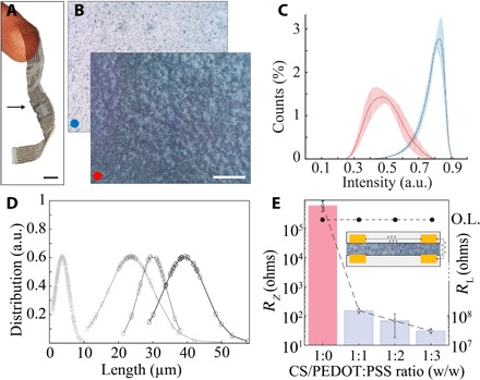
(A) Micrograph of two conformable arrays bonded together by MCP; arrow indicates the bonding area. Scale bar, 500 μm. Photo credit: Patricia Jastrzebska-Perfect, Columbia University. (B) Optical micrographs of blade-coated MCP films. Concentration [% (w/v)] of conducting polymer particles in nonconducting medium of CS, sorbitol, and glycerol is 6.1 (blue dot) or 18 (red dot). Distinct particles are visible in the nonconducting matrix (top right). Scale bar, 100 μm. (C) Pixel intensity distribution (where black = 0) of MCP; concentration [% (w/v)] of PEDOT:PSS particles in blade-coated solution is 6.1 (blue) or 18 (red). Data are represented as mean darkness (n = 6) ± SEM. Note that a higher concentration of particles produces a darker and wider distribution of pixel intensity. a.u., arbitrary units. (D) Optically measured distributions conducting polymer particle size in MCP (from left to right, using 1 and 10 μm, 10 and 20 μm, 20 and 30 μm, and 30 and 40 μm sieves). (E) Vertical (left axis, open circles) resistance of MCP is proportional to conducting polymer particle density in CS (particle size = 40 μm). Inset shows measurement configuration of vertical and horizontal resistances. O.L., overload.
To characterize the conductivity of the MCPs, we prepared composites with various particle densities, including one without particles (control). These composites were sandwiched between two substrates that consisted of multiple horizontally spaced, vertically aligned strips of Au (1 mm wide and 100 μm spacing, 100 nm thick; Fig. 2E, inset). The MCPs exhibited <100-ohm electrical contact resistance between the aligned Au strips. This vertical resistance (RZ) was proportional to particle density, whereas resistance between horizontally spaced Au strips remained high (RL > 108 ohms) (Fig. 2E). These features suggest that the particles remain homogeneously distributed within the MCP when sandwiched between the substrates, without focal coagulation that would cause increased horizontal conduction. Thus, the physical processes used to prepare the MCP offer several key advantages: (i) highly controllable generation of particles with specific size and density; (ii) homogeneous distribution of particles within the composite, even after lamination; (iii) preservation of electrical properties of the conducting polymer; (iv) ability to include additives that enhance electrical performance of the composite; (v) solvent-free synthesis, enhancing compatibility with organic materials; and (vi) scalability for a variety of production volumes (18).
We next tested the ability of MCP to perform the operations described in Fig. 1. First, we examined whether MCP had sufficient anisotropy to form high-density vertical interconnects between electronic components without patterning. We fabricated Au-based electronic pads on rigid (SiO2) and conformable [parylene-C (Pa-C)] substrates with geometrically varying interelectrode spacing. The MCP was deposited onto the bottom substrate using typical solution-processable techniques (spin coating and blade coating) and then covered by the top substrate. Because CS is intrinsically adhesive, MCP established strong mechanical bonds between layers of both rigid and conformable substrates, without requiring elevated temperatures (maximum, 70°C) or application of pressure (figs. S3 and S4). Anisotropy of the interface (A) was determined by calculating the ratio of the horizontal (RL) and vertical (RZ) resistances between the pads (A = RL/RZ; Fig. 3A). Ensuring that the MCP used had a smaller λ than the electrode pitch, we were able to achieve anisotropy values as high as 1010 at 50 μm resolution (Fig. 3B). These anisotropy values were consistent for more than 100 days, highlighting the stability of MCP’s electrical and mechanical bonding (fig. S4).
Fig. 3. MCP creates high-performance anisotropic films, independently addressable transistors, and diodes by varying conducting polymer particle size and density.
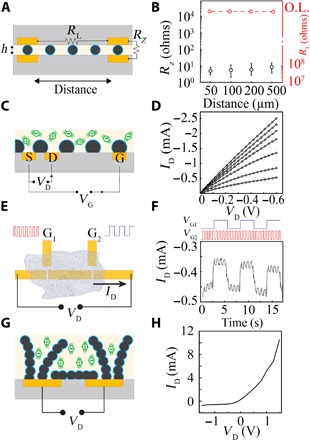
(A) MCP operating as an anisotropic conductive film. λ is smaller than electrode spacing. Scaffolding polymer matrix (light yellow), conducting polymer particles (dark blue), Au contacts (gold), and substrate (gray) are visible. (B) Adjacent MCP-bonded electrodes have consistently low vertical resistance (left axis) and high horizontal resistance (right axis) across a wide range of horizontal electrode pitch. (C) MCP operating as an independently gated transistor. λ is longer than d1 but shorter than d2. Mobile ions (green), and Au contacts forming the source (S), drain (D), and gate (G) are visible. (D) Output characteristics of MCP-based transistor operating in depletion mode (L = 250 μm, W = 5 mm, particle size = 30 μm), with VG varying from 0 to 0.6 V, in increments of 0.1 V (top to bottom). (E) NOR gate generated using un-patterned MCP-based transistors. Input signals are applied at gates 1 and 2 (G1 and G2, respectively). (F) Temporal response of MCP-based NOR gate (L = 100 μm, W = 500 μm, particle size = 30 μm) with gate pulse amplitudes of 0.5 V. (G) MCP operating as a diode. α is substantially less than d1, but λ is approximately equal to d1. (H) Output characteristic of MCP-based diode [same dimensions as (D), particle size = 10 μm].
Next, we made MCP-based independently gated electrochemical transistors by blade-coating MCP onto three Au-based pads (Fig. 3C). This configuration functioned as a depletion-mode, high-transconductance, individually addressable organic electrochemical transistor (OECT). Application of positive gate voltage (VG) to the Au pads directed cations of the ion-conducting scaffolding polymer matrix into the bridging mixed-conducting particles of the channel, resulting in dedoping. The electrical characteristics of the transistor were comparable to those generated by PEDOT:PSS dispersion (Fig. 3D and figs. S5 and S7) (14, 19, 20). We used the independent gating of these devices to create logic circuits with series and parallel connectivity between transistor terminals (such as a NOR gate; Fig. 3E) and found that MCP-based transistors performed the appropriate digital logic (Fig. 3F and fig. S6) over extended time periods in physiological conditions (fig. S5A) (21–24). Therefore, MCP can be used to produce independent transistors that maintain the properties of their constituent conducting polymer without requiring any channel patterning.
Last, we explored the ability of the MCP to operate as a diode. We coated MCP with appropriate α and ρ onto two Au-based pads and applied voltage between the terminals (Fig. 3G). This arrangement created particle chains that contacted both terminals (“bridging particle chains”) and particle chains that contacted one terminal with their free ends omnidirectionally distributed in the ion-conducting scaffolding polymer matrix (“omnidirectional particle chains”). The application of voltage to the terminals resulted in both (i) electronic current through the bridging particle chains and (ii) ionic current in the scaffolding polymer matrix in the region between the omnidirectional particle chains and bridging particle chains. When negative voltage was applied, the omnidirectional chains at the opposite terminal were at positive potentials. The ionic current caused cations of the matrix to dedope the bridging particle chains and lower the charge carrier density. Conversely, when omnidirectional chains were at negative potentials, the bridging particles chains were maximally doped and unaffected by the ionic current within the matrix. Together, these interactions generated the nonlinear voltage-current relationship characteristic of a diode (Fig. 3H). This working mechanism is akin to a diode-connected transistor (25).
We created devices that harnessed the anisotropic properties of MCP to address challenges in physiological signal transmission and biopotential sensing. High–spatiotemporal resolution conformable probes are increasingly being used to acquire signals from biological tissues, and similar resolution rigid electronics exist to process these signals. However, current techniques to enable transmission of signals between the soft probe and hard electronics (thermal bonding or sonic metal-metal bonding, metal/epoxy composite pastes) are neither biocompatible nor scalable and introduce additional rigidity and bulk to the device. We hypothesized that the characteristics of MCP would enable high–spatiotemporal resolution, biocompatible, multichannel electrical contact between soft and hard electronic device components with a facile fabrication process that is adaptable to a wide range of materials. We fabricated conformable (Pa-C) and flexible (polyethylene naphthalate) high-density neural interface devices for integration with flexible [polyethylene terephthalate (PET)] and rigid (flame-retardant glass epoxy, FR4) neural acquisition electronic circuits. MCP was applied to the back end (where the interconnects transform into contact pads) of the probe using a blade coater. MCP formed an adhesive film (through evaporation of excess water) within 120 s at room temperature. We then aligned the mating board (a geometrically matched board containing hard electronics) and established mechanical contact using a manual cotton-based roller with negligible application of pressure (0.15 N). We found that MCP was able to establish a reliable electrical interface between all combinations of conformable, flexible, and rigid neural probes and acquisition electronics (Fig. 4A), permitting higher density connectivity compared to traditional connector or bonding processes (26, 27). To validate the functionality of these MCP-bonded devices, we used them to acquire high–spatiotemporal resolution electrophysiological signals in various experimental conditions. MCP-bonded surface electrocorticography (ECoG) arrays (128 channels; NeuroGrid) (26) and penetrating probes (32 channels) were implanted chronically into freely moving rodents. NeuroGrid recordings demonstrated spatially localized high-gamma oscillations (Fig. 4, B and C) (28, 29), confirming the absence of cross-talk between adjacent channels. Insertion of penetrating probes into the dorsal CA1 of the hippocampus allowed high-fidelity acquisition of characteristic high-frequency hippocampal oscillations (ripples, 100 to 250 Hz; Fig. 4D) (30, 31) and individual neuronal action potentials (Fig. 4D, inset). Together, these results demonstrate that MCP bonding can be used to create scalable, multichannel neural interface devices that are capable of acquiring signals at the spatiotemporal resolution of individual neurons (figs. S5A and S9).
Fig. 4. MCP creates an anisotropic interface for high–spatiotemporal resolution electrophysiologic signal transmission.
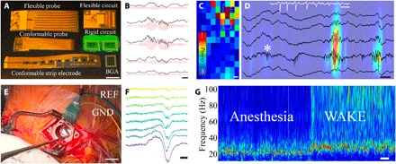
(A) Photograph of conformable, flexible, and rigid neural probes with electronic circuits that can be bonded together using MCP to acquire neurophysiological signals in vivo. Scale bar, 5 mm. BGA, ball grid array. Photo credit: Dion Khodagholy, Columbia University. (B) High gamma oscillations are differentiable across electrodes of an MCP-bonded array placed on cortical surface of a freely moving rat [unfiltered local field potential (LFP) traces (black) and corresponding filtered traces (red, 60 to 100 Hz)]. Scale bar, 40 ms. (C) Trigger-averaged gamma band power is spatially confined across array placed on cortical surface of a freely moving rat. Scale bar, 1 mm. The white dashed rectangle indicates the electrodes that generated the traces in (B). (D) MCP-bonded flexible probe inserted into rat hippocampus permits recording of characteristic ripple oscillations in dorsal CA1 [sample wide-band traces (black, 0.1 to 20 kHz) superimposed on a heat map highlighting the instantaneous power in the ripple band (100 to 150 Hz); scale bar, 50 ms] as well as individual action potential waveforms (burst firing of putative pyramidal cell, white trace, zoomed in from location denoted by white star, 0.1 to 20 kHz; scale bar, 5 ms). Color bar same as (C). (E) Intraoperative photograph showing conformable MCP-bonded neural probe on the surface of human cortex with associated amplifier circuits. Scale bar, 10 mm. Photo credit: Dion Khodagholy, Columbia University. REF, reference; GND, ground. (F) Sample wide-band LFP (0.1 to 1250 Hz) acquired during intraoperative human recording demonstrating spatially diverse activity patterns acquired by MCP-bonded neural probe. Scale bar, 100 ms. (G) Spectrogram of neural data acquired by MCP-bonded neural probe revealing transition from anesthetized to awake state intraoperatively. Scale bar, 10 s. Color bar same as (C).
We also leveraged the biocompatibility of MCP to generate neural interface devices for intraoperative neural recording in human patients undergoing implantation of deep brain stimulation (DBS) electrodes. During a DBS procedure, clinical electrodes are inserted through a burr hole (14-mm diameter) to reach the appropriate subcortical target (32, 33). We recorded from the exposed cortex with our MCP-bonded device during the surgical procedure. To record from the small exposed cortical area, the probe and amplifier components must be miniaturized and flexible, precluding use of conventional surface ECoG arrays. We demonstrated that MCP-bonded NeuroGrids could be placed within the burr hole (Fig. 4E, figs. S10 and S11, and movie S1) and acquired spatially resolved, high–signal-to-noise-ratio (SNR) neurophysiological data in the intraoperative environment. These data revealed characteristic signals associated with transition from anesthesia to waking, as well as localized epochs of gamma oscillations (Fig. 4, F and G). Thus, MCP-bonded neural interface devices can be safely and effectively translated to use in human patients.
Next, we investigated MCP for direct biopotential sensing. Because MCP is biocompatible, with tunable electronic and ionic properties and a versatile fabrication process, we hypothesized that it could effectively interface directly with the human body and enable high–spatiotemporal resolution, mechanically stable sensing (Fig. 5A, left, and figs. S11 to S13). The bonding strength and electrochemical impedance of the MCP interface with tissue was enhanced by d-sorbitol, a biocompatible sugar alcohol, within the composite. The d-sorbitol facilitates uptake and maintenance of water within the matrix (21, 34). Conventional electrodes designed to acquire electrophysiologic signals from the skin typically rely on ionic gels to form an appropriate impedance interface with the skin. These gels are not amenable to patterning, and their spread across the skin surface is difficult to control, limiting the spatial resolution of activity that can be acquired noninvasively. When higher-resolution signals are required, such as with clinical electromyography (EMG), needle electrodes are inserted through the skin. Au-based electrodes coated with a layer of MCP (200 μm diameter) were placed over the biceps muscle and wrist of healthy participants (n = 3) to acquire EMG and electrocardiography (ECG) signals (Fig. 5A, right). The SNR of both EMG and ECG acquired by MCP-based interface were comparable with that of conventional, larger gel-based electrodes (Fig. 5A, bottom, and figs. S11 to S13). To evaluate the possibility of higher–spatial resolution biopotential acquisition, we fabricated a conformable array of electrodes (64 channels, 250 μm electrode diameter, and 4 mm by 7 mm effective surface area), applied a thin layer of MCP to a similar surface area of skin over the wrist of a human participant, and placed the array on top. Voluntary flexion of each finger resulted in differentiable patterns of neural activity across the electrode array (Fig. 5B). In addition, it was possible to localize independent nerve action potentials with well-defined waveforms and firing rates (Fig. 5C). Multiple adjacent electrodes on the array captured the same action potential with waveforms reflecting the source and propagation of the activity (Fig. 5D and fig. S14). Simple application of a biocompatible MCP layer enables high–spatiotemporal resolution, noninvasive acquisition of electrophysiologic potentials from human skin.
Fig. 5. MCP creates an anisotropic interface for high spatiotemporal biopotential sensing.
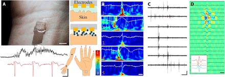
(A) Micrograph of a high-density, conformable EMG array adhered to the wrist of a human participant using MCP (top left; scale bar, 10 mm). Cross-sectional schematic (top right) comparing gel (upper) and MCP interfaces (lower) between skin and electronics. Sample traces of MCP-acquired EMG (black) and ECG (red) signals are shown with their corresponding recording site on biceps and the wrist. Scale bar, 1 s; 4 mV. Photo credit: George Spyropoulos, Columbia University. (B) Spectrograms of EMG signals acquired using MCP-adhered conformable array placed over the wrist (bottom left schematic) reveal distinct patterns during voluntary flexion of each finger. Scale bar, 80 ms. (C) MCP-adhered conformable array permits noninvasive recording of independent nerve action potentials. Scale bar, 100 ms; 4 mV. (D) Current source density heat map of a sample nerve action potential from (C) as visualized across adjacent electrodes reveals the source localization and propagation. Scale bar, 5 ms. Color bar same as (B).
DISCUSSION
In this study, we developed an innovative, soft, biocompatible composite material (MCP) that can serve as various electronic components, depending on the size and density of constituent particles. The key components of MCP are conducting polymer particles and an ion-conducting scaffolding polymer matrix, enabling high conductivity and ionic interactions through de/doping. The physical processes used to prepare the MCP are scalable, solvent free and preserve the electrical properties of the conducting polymer. These processes are likely adaptable to other organic materials and could enable use of materials previously inaccessible to device fabrication because of their inability to readily form films. We demonstrated that the combination of MCP composed of PEDOT:PSS particles and CS with simply patterned electrical terminals can be used to create functional anisotropic films, independently addressable transistors, resistors, and diodes. The composite nature of MCP endows it with multifunctional properties that can simplify device architectures that previously required multiple material interfaces, such as diodes.
MCP addresses key challenges in electrophysiological signal acquisition and processing by permitting anisotropic, high–spatiotemporal resolution sensing and transmission. We bonded soft and rigid electronics with a simply applied layer of MCP, thereby eliminating the need for bulky or nonbiocompatible interfaces between these device components. We verified the fidelity of signal transmission via MCP across the physiologic spectrum (0.1 Hz to 20 kHz). Further experimentation regarding the effect of scaffolding matrix ion conductivity on parasitic capacitance across adjacent contacts is required to extend the signal transmission bandwidth to ranges suitable for digital communication. Forces required to delaminate MCP-bonded substrates (approximately 25 N) also exceed those encountered during in vivo implantation and data acquisition, establishing mechanical stability of these devices. MCP substantially reduced the backend footprint of neural interface devices, permitting recording of high-quality neurophysiological data from the surface of the human brain through a small opening in the skull. These capabilities are critical as advances in neurosurgical tools and equipment allow for minimally invasive procedures, requiring sensing devices to miniaturize to remain compatible (35). Because smaller, softer bioelectronic devices are more versatile in their surgical placement, previously inaccessible data can potentially be made available, improving diagnostics.
We also used MCP to directly interface with human skin, overcoming the trade-off between electrode size and impedance to allow high-fidelity acquisition of ECG and EMG, as well as sensing of spatially localized nerve action potentials noninvasively from a small surface area. Compared to clinical needle EMG, MCP-based EMG has similar amplitude range (0 to 10 mV) and SNR (5 to 30 dB) but can offer multiple recording sites from the same muscle (36) without requiring penetration through the skin. Noninvasive electrodes for biopotential recording use electrolyte gels or soft microstructures to decrease the electrode-skin interface impedance, but spatial resolution is on the order of centimeters (37). The use of MCP as an interface for biopotential sensing could increase the amount and quality of data extracted with noninvasive methods and could potentially eliminate the need for some types of invasive recordings. Furthermore, the ability to create MCP-based integrated circuits could be leveraged to enhance signal quality by providing differential amplification with high common-mode rejection. Mechanical stability of noninvasive biopotential sensors is important for procedures that require long-term data acquisition. MCP films are stable in aqueous environments and exhibit high stress/strain tolerance, suggesting that they could provide a stable mechanical interface with skin, but further experimentation is necessary to determine the optimal parameters for such applications. Overall, MCP has the potential to become a critical component of bioelectronics, from wearable miniaturized sensors to responsive stimulators, enhancing our ability to harness these devices to benefit health and treat disease.
MATERIALS AND METHODS
Materials
PEDOT:PSS (Clevios PH1000) was acquired from Heraeus. Ethylene glycol, CS (50 to 190 kDa, 75 to 85% deacetylated), (3-glycidyloxypropyl)trimethoxysilane (GOPS), 4-dodecyl benzene sulfonic acid (DBSA), d-sorbitol (BioUltra ≥99.5%), glycerol, phosphate-buffered saline (PBS) tablets, poly(styrene sulfonate), polyvinyl alcohol (PVA), and gelatin (from bovine skin) were purchased from Sigma-Aldrich. Cell strainers (PET-mesh, pore diameters of 10, 20, 30, or 40 μm) were purchased from pluriSelect. Tensive conductive adhesive gel was purchased from Parker Laboratories.
Particle preparation
High-conductivity PEDOT:PSS was prepared by mixing 80% PEDOT:PSS, 20% ethylene glycol, and 0.6% DBSA (all v/v). High-conductivity PEDOT:PSS mixed with 1% (v/v) of GOPS was cast into a glass petri dish and dehydrated overnight at 120°C in a well-ventilated environment. The resulting film was scraped from the dish with a stainless steel blade and cut into small fragments. Film fragments were suspended in isopropyl alcohol (IPA) and crushed overnight in a bead mill using stainless steel beads ranging from 3.17 to 6.35 mm in diameter. The particle suspension was serially filtered using PET-mesh cell strainers with pores ranging from 1 to 40 μm in diameter. The size-filtered particles were resuspended in IPA, and the suspensions were sonicated overnight. The suspension was allowed to precipitate, and excess IPA was removed.
Polymer/particle blend preparation
CS was dissolved in 2% (v/v) acetic acid, filtered using 40 μm cell strainers, and then concentrated via dehydration to 2.5% (w/v). A 40% (w/v) d-sorbitol solution was prepared with the CS stock. PEDOT:PSS particles were added dropwise into CS-sorbitol under constant stirring to produce a 2.5:1 (unless otherwise specified) PEDOT:PSS/CS by weight suspension. The suspension was dehydrated to 10% (w/v) of PEDOT:PSS (unless otherwise specified) in final solution. A control solution was prepared following the same method, except without the addition of PEDOT:PSS particles. For biopotential recordings, CS solution based on 1× PBS was used.
Anisotropic bonding characterization
A film (MCP or CS-sorbitol control) was blade-coated onto a glass electrode-patterned substrate. The film was dried for 60 s at 70°C. A PET electrode-patterned substrate was vertically aligned over the glass substrate (whereby each substrate’s electrodes were positioned directly on top of the other substrate’s electrodes) and bonded. The bonded sample was roll-pressed to ensure film uniformity and allowed to fully cool. The horizontal and vertical resistances between electrodes were measured at various points in time for multiple samples.
Transistor/diode
MCP with particle size smaller than Au-based microfabricated terminals was used as channel material. A 4-mm-thick film of 10% gelatin prepared using 1× PBS solution was then laminated on top of the channel to maintain film hydration for an extended period of time.
Stress versus strain test
A CS-PVA solution was prepared by mixing equal volumes of 8% (w/v) PVA (in deionized water) and 2.5% (w/v) CS. An MCP solution was prepared by mixing 7% (w/v) PEDOT:PSS particles into the CS-PVA solution. The MCP solution was poured into a petri dish and dehydrated overnight at 70°C to form a 0.08-mm-thick film. Each end of a 7-mm-wide, 2-cm-long strip of the film was enclosed between two glass slides, leaving a 7 mm by 5 mm exposed region in the center of the strip. Each enclosed end was secured with a clip. One clip was attached to a Nextech Digital Force Gauge. The other clip was grasped to stretch the film.
Electrical characterization
Current-voltage characteristics were obtained using two channels of a Keysight B2902A Precision Source/Measurement Unit. The first channel (VD) applied a linear sweep from 0 to −0.6 V or 1.2 to −1.2 V. The second channel (VG) (if required) applied a constant voltage from 0 to 0.6 V, incrementing in steps of 0.1 V, with 500-ms duration measurement per point. Electrical characteristics were measured using platinum or Ag/AgCl gate electrodes. Temporal responses of OECTs and OECT-based logic gates to pulse trains produced simultaneously by a Keysight B2902A and Keysight 33500B Series waveform generator, under constant applied VD from a Keysight B2902A, were recorded using the Keysight B2902A.
Neural probe fabrication
The fabrication and patterning of Pa-C and PEDOT:PSS-based conformable surface arrays have been discussed in previous publications (21, 26, 27, 38, 39). A proximity contact lithography system (Suss MA-6) was used to pattern Pa-C, Au, Pt, Ti, and PEDOT:PSS films. First, Pa-C was deposited using a chemical vapor deposition (SCS Labcoter 2) to a thickness of 2 μm. We used 3-(trimethoxysilyl) propyl methacrylate as an adhesion promoter and a dilute solution of industrial cleaner (Micro-90) as an anti-adhesion agent. Next, the film was patterned with a 4.6-μm-thick layer of AZ9260 photoresist and dry-etched with a reactive ion-etching process [180 W, 50–standard cubic centimeters per minute (sccm) O2, 3-sccm SF6, and 2-sccm CF4 for 18 min; Oxford 80 Plus]. A liftoff process was used to pattern metal pads and interconnects. AZ nLOF 2020 (chemically amplified negative resist) was spin-coated on the Pa-C film [5500 revolutions per minute (rpm)], baked at 115°C for 60 s, exposed using Suss MA-6, and lastly developed (AZ Developer). With the use of an e-beam metal evaporator (angstrom at 2.10−6 bars), metallic layers of Ti (10 nm) and Au (150 nm) were deposited. Liftoff was performed using 1165 stripper (2 hours). To enhance the conductivity of PEDOT:PSS, a mixture of PEDOT:PSS aqueous dispersion (PH-1000 from H. C. Stark) and ethylene glycol (ratio of 20:5 ml) was prepared and mixed with dodecylbenzenesulfonic acid (100 ml per 50 ml) and GOPS [1% (w/v)] to adjust surface energy and cross-link, respectively. The resulting dispersion was spin-coated in two steps with a soft bake in between (120°C, 60 s) at 650 rpm. The films were subsequently baked at 140°C for 1 hour and then immersed in deionized water to remove any excess low–molecular weight compounds. The electrodes were characterized in vitro using PBS solution. A substantially larger Au plate compared to electrode geometry served as the reference electrode for impedance spectroscopy and measurements.
Pixel distribution of MCP films
MCP [6.1 or 18% (w/v) particles and 0.83% (w/v) CS in solution containing 33% (v/v) glycerol] was prepared and blade-coated onto a clean glass substrate. The film was imaged using an upright bright-field microscope at ×50 magnification. To determine distribution of pixels within the films, each sample image (n = 6) was first converted to gray scale. The pixels of the gray scale image were binned into 256 bins (1 bin per RGB value of range 0 to 255). The mean and SE of counts per bin, normalized by total pixels, were computed. All images were processed using the MATLAB Image Processing Toolbox.
Particle size
Size-filtered particles were drop-casted onto a clean glass slide and imaged using an upright, bright-field microscope at ×50 magnification. Each sample image (n = 5) was converted to gray scale. Image contrast was increased by saturating the top and bottom 1% of pixel values. The image was converted to a binary form by discarding all pixels greater than a threshold set at the point that produced the minimum number of connected regions. The area and smallest diameter of each connected region within the binary image was determined. Areas with substantially less than the minimum surface area possible for each filtering range (e.g., for 10 to 20 μm filter range, 1 μm by 1 μm pixel area) were considered to be noise and excluded from the dataset. The mean and SD of each range were computed and used to plot the range’s normal (Gaussian) distribution. All images were processed using the MATLAB Image Processing Toolbox.
ECG and EMG recordings
ECG and EMG recordings were performed on healthy participants (n = 3). Before each recording, the skin at the recording site was cleaned using soap and 50% (v/v) IPA. A 1 cm by 1 cm region of skin at each recording site was coated with a thin layer of MCP using a brush, and the layer was allowed to dry at room temperature for 30 s before a Pa-C substrate probe was placed on the coated skin. Signals were acquired by sampling at 20 kHz, using a custom board incorporating an RHD2164 die (Intan Technologies). Signals were visualized in real time with the RHD2000 Interface Software. Data were stored for analysis in a 16-bit format and analyzed with MATLAB (MathWorks).
Rodent electrophysiological recordings
All the animal experiments were approved by the Institutional Animal Care and Use Committee of Columbia University. Depth and surface arrays were used in cortical implantations in male Long Evans rats (250 to 350 g; 8 to 11 weeks of age, n = 3). Rats were housed in a regular 12-hour/12-hour light/dark cycle throughout the course of experimentation. Rats were housed in pairs before surgical procedure but separated after intracranial implantation was performed. Rats used in these experiments had no previous history of experimentation of any kind. The animals were initially anesthetized with 2% isoflurane and maintained under anesthesia with 0.75 to 1% isoflurane during the surgery. A 5 mm by 9 mm craniotomy was performed on the right hemisphere; the NeuroGrid was placed on the exposed cortical surface. The craniotomy was covered by Gelfoam and sealed using a medical grade silicone. Implantable flexible probes were inserted to depth of 2 mm (AP, 3.50 mm; ML, 3.00 mm) using a 50 μm diameter tungsten wire as a guide.
Intraoperative human patient recordings
Intraoperative human patient recordings were approved by the Institutional Review Board (IRB) at Baylor College of Medicine (BCM), and the surgical procedures were performed at Baylor St. Luke’s Medical Center (BSLMC). Patients requiring burr hole creation for placement of DBS electrodes were eligible for the study (n = 4). Informed written consent was obtained from all patients for all aspects of the protocol, including publication of photos. NeuroGrids laminated to amplifiers using MCP, and associated cables were sterilized using a conventional ethylene oxide gas sterilization protocol performed by the central sterilization facility of BSLMC. To prevent mechanical damage to the NeuroGrids during the sterilization procedure, devices were sutured to custom sterilization boxes (FR4) and released for use only in the operating room. Recordings lasted for a maximum of 30 min and were performed either under anesthesia or awake as determined by the clinical protocol, attending neurosurgeon, and anesthesiologist. Placement of the array was guided by location of the burr hole required for clinical diagnostic and therapeutic procedures and by advice of the attending neurosurgeons.
Supplementary Material
Acknowledgments
We thank E. Stavrinidou (University of Linköping), G. Malliaras (Cambridge University), M. Gonzalez, J. Yu, J. Vichiconti, N. Porecki-Shamay, and N. Ariel-Sternberg (CNI) and all Khodagholy and Gelinas laboratory members for their support. We thank J. Montier (Baylor College) for managing the IRB protocol and administrative affairs of intraoperative recordings at BCM. Funding: This work was supported by Columbia University, School of Engineering and Applied Science, as well as Columbia University Medical Center, Department of Neurology and Institute for Genomic Medicine. The device fabrication was performed at (i) Columbia Nano Initiative and (ii) Cornell NanoScale Facility (CNF), a member of the National Nanotechnology Coordinated Infrastructure (NNCI), which is supported by the National Science Foundation (grant ECCS-1542081). G.D.S. is supported through the Human Frontiers Postdoctoral Fellowship Program. This work was supported by the NIH (1U01NS108923-01, 1U01NS099705), NSF CAREER (1944415), CURE Taking Flight Award, and Columbia School of Engineering. Author contributions: D.K., J.N.G., and P.J.-P. conceived the project. P.J.-P., D.K., and G.D.S. designed, developed, fabricated, and characterized the devices and materials. C.C., G.D.S., D.K., and P.J.-P. fabricated neural probes for rodent and human recordings. P.J.-P. performed human ECG and EMG recordings. D.K., J.N.G., Z.Z., A.V., and S.A.S. did the electrophysiology in vivo human and rodent experiments and analysis. O.J.R. performed rodent intracranial surgery and in vivo electrophysiologic recordings. A.V. and S.A.S. were the attending neurosurgeons and conducted the intraoperative recordings. D.K., J.N.G., and P.J.-P. wrote the paper with input from all authors. Competing interests: The authors declare that they have no competing interests. Data and materials availability: All data needed to evaluate the conclusions in the paper are present in the paper and/or the Supplementary Materials. Additional data related to this paper may be requested from the authors.
SUPPLEMENTARY MATERIALS
Supplementary material for this article is available at http://advances.sciencemag.org/cgi/content/full/6/17/eaaz6767/DC1
REFERENCES AND NOTES
- 1.Jeong J.-W. W., Shin G., Park S. I., Yu K. J. J., Xu L., Rogers J. A. A., Soft materials in neuroengineering for hard problems in neuroscience. Neuron 86, 175–186 (2015). [DOI] [PubMed] [Google Scholar]
- 2.Chen R., Canales A., Anikeeva P., Neural recording and modulation technologies. Nat. Rev. Mater. 2, 16093 (2017). [DOI] [PMC free article] [PubMed] [Google Scholar]
- 3.Someya T., Bao Z., Malliaras G. G., The rise of plastic bioelectronics. Nature 540, 379–385 (2016). [DOI] [PubMed] [Google Scholar]
- 4.Berggren M., Richter-Dahlfors A., Organic Bioelectronics. Adv. Mater. 19, 3201–3213 (2007). [Google Scholar]
- 5.Crone B., Dodabalapur A., Lin Y.-Y., Filas R. W., Bao Z., LaDuca A., Sarpeshkar R., Katz H. E., Li W., Large-scale complementary integrated circuits based on organic transistors. Nature 403, 521–523 (2000). [DOI] [PubMed] [Google Scholar]
- 6.Kaltenbrunner M., Sekitani T., Reeder J., Yokota T., Kuribara K., Tokuhara T., Drack M., Schwödiauer R., Graz I., Bauer-Gogonea S., Bauer S., Someya T., An ultra-lightweight design for imperceptible plastic electronics. Nature 499, 458–463 (2013). [DOI] [PubMed] [Google Scholar]
- 7.Kim S. H., Hong K., Xie W., Lee K. H., Zhang S., Lodge T. P., Frisbie C. D., Electrolyte-gated transistors for organic and printed electronics. Adv. Mater. 25, 1822–1846 (2013). [DOI] [PubMed] [Google Scholar]
- 8.Krook-Magnuson E., Gelinas J. N., Soltesz I., Buzsáki G., Neuroelectronics and biooptics: Closed-loop technologies in neurological disorders. JAMA Neurol. 72, 823–829 (2015). [DOI] [PMC free article] [PubMed] [Google Scholar]
- 9.Fang H., Zhao J., Yu K. J., Song E., Farimani A. B., Chiang C.-H., Jin X., Xue Y., Xu D., Du W., Seo K. J., Zhong Y., Yang Z., Won S. M., Fang G., Choi S. W., Chaudhuri S., Huang Y., Alam M. A., Viventi J., Aluru N. R., Rogers J. A., Ultrathin, transferred layers of thermally grown silicon dioxide as biofluid barriers for biointegrated flexible electronic systems. Proc. Natl. Acad. Sci. U.S.A. 113, 11682–11687 (2016). [DOI] [PMC free article] [PubMed] [Google Scholar]
- 10.Fang H., Yu K. J., Gloschat C., Yang Z., Song E., Chiang C.-H., Zhao J., Won S. M., Xu S., Trumpis M., Zhong Y., Han S. W., Xue Y., Xu D., Choi S. W., Cauwenberghs G., Kay M., Huang Y., Viventi J., Efimov I. R., Rogers J. A., Capacitively coupled arrays of multiplexed flexible silicon transistors for long-term cardiac electrophysiology. Nat. Biomed. Eng. 1, 0038 (2017). [DOI] [PMC free article] [PubMed] [Google Scholar]
- 11.Paulsen B. D., Tybrandt K., Stavrinidou E., Rivnay J., Organic mixed ionic–electronic conductors. Nat. Mater. 19, 13–26 (2020). [DOI] [PubMed] [Google Scholar]
- 12.Zozoulenko I., Singh A., Singh S. K., Gueskine V., Crispin X., Berggren M., Polarons, bipolarons, and absorption spectroscopy of PEDOT. ACS Appl. Polym. Mater. 1, 83–94 (2019). [Google Scholar]
- 13.Crispin X., Jakobsson F. L. E., Crispin A., Grim P. C. M., Andersson P., Volodin A., van Haesendonck C., Van der Auweraer M., Salaneck W. R., Berggren M., The origin of the high conductivity of poly(3,4-ethylenedioxythiophene)−poly(styrenesulfonate) (PEDOT−PSS) plastic electrodes. Chem. Mater. 18, 4354–4360 (2006). [Google Scholar]
- 14.Khodagholy D., Rivnay J., Sessolo M., Gurfinkel M., Leleux P., Jimison L. H., Stavrinidou E., Herve T., Sanaur S., Owens R. M., Malliaras G. G., High transconductance organic electrochemical transistors. Nat. Commun. 4, 2133 (2013). [DOI] [PMC free article] [PubMed] [Google Scholar]
- 15.Wang S., Sun C., Guan S., Li W., Xu J., Ge D., Zhuang M., Liu T., Ma X., Chitosan/gelatin porous scaffolds assembled with conductive poly(3,4-ethylenedioxythiophene) nanoparticles for neural tissue engineering. J. Mater. Chem. B 5, 4774–4788 (2017). [DOI] [PubMed] [Google Scholar]
- 16.Meng X., Wang Z., Wang L., Pei M., Guo W., Tang X., Electrosynthesis of pure poly(3,4- ethylenedioxythiophene) (PEDOT) in chitosan-based liquid crystal phase. Electron. Mater. Lett. 9, 605–608 (2013). [Google Scholar]
- 17.Ravi Kumar M. N. V., A review of chitin and chitosan applications. React. Funct. Polym. 46, 1–27 (2000). [Google Scholar]
- 18.Sani N., Robertsson M., Cooper P., Wang X., Svensson M., Ersman P. A., Norberg P., Nilsson M., Nilsson D., Liu X., Hesselbom H., Akesso L., Fahlman M., Crispin X., Engquist I., Berggren M., Gustafsson G., All-printed diode operating at 1.6 GHz. Proc. Natl. Acad. Sci. U.S.A. 111, 11943–11948 (2014). [DOI] [PMC free article] [PubMed] [Google Scholar]
- 19.Rivnay J., Inal S., Salleo A., Owens R. M., Berggren M., Malliaras G. G., Organic electrochemical transistors. Nat. Rev. Mater. 3, 17086 (2018). [Google Scholar]
- 20.Bernards D. A., Malliaras G. G. G., Steady-state and transient behavior of organic electrochemical transistors. Adv. Funct. Mater. 17, 3538–3544 (2007). [Google Scholar]
- 21.Spyropoulos G. D., Gelinas J. N., Khodagholy D., Internal ion-gated organic electrochemical transistor: A building block for integrated bioelectronics. Sci. Adv. 5, eaau7378 (2019). [DOI] [PMC free article] [PubMed] [Google Scholar]
- 22.Arias A. C., MacKenzie J. D., McCulloch I., Rivnay J., Salleo A., Materials and applications for large area electronics: Solution-based approaches. Chem. Rev. 110, 3–24 (2010). [DOI] [PubMed] [Google Scholar]
- 23.Braga D., Erickson N. C., Renn M. J., Holmes R. J., Frisbie C. D., High-transconductance organic thin-film electrochemical transistors for driving low-voltage red-green-blue active matrix organic light-emitting devices. Adv. Funct. Mater. 22, 1623–1631 (2012). [Google Scholar]
- 24.Lee J., Panzer M. J., He Y., Lodge T. P., Frisbie C. D., Ion gel gated polymer thin-film transistors. J. Am. Chem. Soc. 129, 4532–4533 (2007). [DOI] [PubMed] [Google Scholar]
- 25.A. S. Sedra, D. E. A. S. Sedra, K. C. Smith, K. C. Smith, Microelectronic Circuits (Oxford Univ. Press, 1998). [Google Scholar]
- 26.Khodagholy D., Gelinas J. N., Thesen T., Doyle W., Devinsky O., Malliaras G. G., Buzsáki G., NeuroGrid: Recording action potentials from the surface of the brain. Nat. Neurosci. 18, 310–315 (2015). [DOI] [PMC free article] [PubMed] [Google Scholar]
- 27.Khodagholy D., Gelinas J. N., Zhao Z., Yeh M., Long M., Greenlee J. D., Doyle W., Devinsky O., Buzsáki G., Organic electronics for high-resolution electrocorticography of the human brain. Sci. Adv. 2, e1601027 (2016). [DOI] [PMC free article] [PubMed] [Google Scholar]
- 28.Sirota A., Montgomery S., Fujisawa S., Isomura Y., Zugaro M., Buzsaki G., Buzsáki G., Entrainment of neocortical neurons and gamma oscillations by the hippocampal theta rhythm. Neuron 60, 683–697 (2008). [DOI] [PMC free article] [PubMed] [Google Scholar]
- 29.Khodagholy D., Gelinas J. N., Buzsáki G., Learning-enhanced coupling between ripple oscillations in association cortices and hippocampus. Science 358, 369–372 (2017). [DOI] [PMC free article] [PubMed] [Google Scholar]
- 30.Buzsáki G., Hippocampal sharp wave-ripple: A cognitive biomarker for episodic memory and planning. Hippocampus 25, 1073–1188 (2015). [DOI] [PMC free article] [PubMed] [Google Scholar]
- 31.Buzsaki G., Horvath Z., Urioste R., Hetke J., Wise K., High-frequency network oscillation in the hippocampus. Science 256, 1025–1027 (1992). [DOI] [PubMed] [Google Scholar]
- 32.Mian M. K., Campos M., Sheth S. A., Eskandar E. N., Deep brain stimulation for obsessive-compulsive disorder: Past, present, and future. Neurosurg. Focus 29, E10 (2010). [DOI] [PubMed] [Google Scholar]
- 33.Benninger D., Schüpbach M., Deep brain stimulation. Ther. Umschau 75, 425–431 (2018). [DOI] [PubMed] [Google Scholar]
- 34.Spyropoulos G. D., Ramirez Quiroz C. O., Salvador M., Hou Y., Gasparini N., Schweizer P., Adams J., Kubis P., Li N., Spiecker E., Ameri T., Egelhaaf H.-J., Brabec C. J., Organic and perovskite solar modules innovated by adhesive top electrode and depth-resolved laser patterning. Energ. Environ. Sci. 9, 2302–2313 (2016). [Google Scholar]
- 35.Grunert P., From the idea to its realization: The evolution of minimally invasive techniques in neurosurgery. Minim. Invasive Surg. 2013, 171369 (2013). [DOI] [PMC free article] [PubMed] [Google Scholar]
- 36.Reaz M. B. I., Hussain M. S., Mohd-Yasin F., Techniques of EMG signal analysis: Detection, processing, classification and applications. Biol. Proced. Online 8, 11–35 (2006). [DOI] [PMC free article] [PubMed] [Google Scholar]
- 37.Merletti R., Farina D., Analysis of Intramuscular electromyogram signals. Philos. Trans. R. Soc. A Math. Phys. Eng. Sci. 367, 357–368 (2008). [DOI] [PubMed] [Google Scholar]
- 38.Khodagholy D., Doublet T., Gurfinkel M., Quilichini P., Ismailova E., Leleux P., Herve T., Sanaur S., Bernard C., Malliaras G. G., Highly conformable conducting polymer electrodes for in vivo recordings. Adv. Mater. 23, H268–H272 (2011). [DOI] [PubMed] [Google Scholar]
- 39.Sessolo M., Khodagholy D., Rivnay J., Maddalena F., Gleyzes M., Steidl E., Buisson B., Malliaras G. G., Easy-to-fabricate conducting polymer microelectrode arrays. Adv. Mater. 25, 2135–2139 (2013). [DOI] [PubMed] [Google Scholar]
Associated Data
This section collects any data citations, data availability statements, or supplementary materials included in this article.
Supplementary Materials
Supplementary material for this article is available at http://advances.sciencemag.org/cgi/content/full/6/17/eaaz6767/DC1