Abstract
Single‐layer and multi‐layer 2D polyimine films have been achieved through interfacial synthesis methods. However, it remains a great challenge to achieve the maximum degree of crystallinity in the 2D polyimines, which largely limits the long‐range transport properties. Here we employ a surfactant‐monolayer‐assisted interfacial synthesis (SMAIS) method for the successful preparation of porphyrin and triazine containing polyimine‐based 2D polymer (PI‐2DP) films with square and hexagonal lattices, respectively. The synthetic PI‐2DP films are featured with polycrystalline multilayers with tunable thickness from 6 to 200 nm and large crystalline domains (100–150 nm in size). Intrigued by high crystallinity and the presence of electroactive porphyrin moieties, the optoelectronic properties of PI‐2DP are investigated by time‐resolved terahertz spectroscopy. Typically, the porphyrin‐based PI‐2DP 1 film exhibits a p‐type semiconductor behavior with a band gap of 1.38 eV and hole mobility as high as 0.01 cm2 V−1 s−1, superior to the previously reported polyimine based materials.
Keywords: 2D polymers, imine-based COFs, interfacial synthesis, photoconductivity, semiconductors
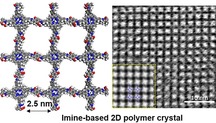
Three crystalline imine‐based 2D polymer films are prepared by surfactant‐monolayer‐assisted interfacial synthesis (SMAIS). The synthetic PI‐2DP films feature polycrystalline multilayers with tunable thickness from 6 to 200 nm and large crystalline domains (100–150 nm in size) and exhibit p‐type semiconductor behavior with a band gap of 1.38 eV.
Introduction
Imine linkage formed by the condensation of an aldehyde and amine has been widely employed for the synthesis of two‐dimensional (2D) and 3D covalent organic frameworks (COFs).1 Due to their high chemical/thermal stability,2 porosity3 and crystallinity,4 imine COFs have attracted considerable attention over the past decade with promising applications in gas storage,5 ion separation,6 semiconductors,7 proton conduction,8 luminescence,9 catalysis and energy conversion.10 However, most of the reported imine‐based COFs have been successfully synthesized in the form of polycrystalline powders. Therefore, incorporation of these insoluble COF powders into thin film electronic devices represents a formidable challenge. To address these issues, considerable progress has been made in developing methods for the synthesis of 2D COF films/nanosheets or single‐/few‐layer 2D polymers including top‐down exfoliation, bottom‐up on‐surface synthesis and interfacial synthesis methods.11 In particular, air–water and liquid–liquid interfaces assisted synthesis offers a reliable pathway to prepare large‐area, single‐/few‐layer 2D polymers which can be easily transferred directly from the interface to various substrates for further characterization and device fabrication.12, 13, 14 For instance, large‐area, imine‐based 2D COF films (polyTB) with varied thickness from ≈2 to 200 nm were prepared at the DMF/air interface, which could function as a semiconductor layer in a field‐effect transistor (FET) device and exhibited a charge carrier mobility of 3.0×10⁻⁶ cm−2 V−1 s−1.15 We have previously explored the synthesis of polyimine‐based 2DPs (PI‐2DPs) at the air–water and liquid–liquid interfaces, which resulted in free‐standing, single‐ and multi‐layer films,14 respectively. Then PI‐2DP was integrated as an active semiconducting layer in a thin film transistor which displayed a mobility of 1.3×10⁻⁶ cm−2 V−1 s−1. Besides the intrinsic low in‐plane conjugation of polyimine, the low mobility can be majorly attributed to the defect densities and small crystalline domain sizes (≈10–20 nm) of the resultant 2D polyimine films. It remains challenging to further improve the crystallinity of PI‐2DPs via such interfacial synthesis due to the lack of control over the ordered arrangement of the precursor monomers at the interface. Moreover, many factors govern the performance of electroactive layers, among which the growth of long‐range ordered crystalline 2D COF/2D polymer films plays a key role in influencing the charge‐carrier transport properties.16 Therefore, considerable improvements in the synthetic methods are required to prepare highly crystalline 2D polymer films to realize their full potential in electronic/optoelectronic devices.
Very recently, our group reported a surfactant‐monolayer‐assisted interfacial synthesis (SMAIS) of few‐layer 2D polyimide and 2D polyamide films on water surface.17 Nevertheless, the achieved 2D polyimide film showed abundant amorphous areas (≈40 % ratio) interconnected within crystalline domains.
In this work, we demonstrated the efficient synthesis of large‐area, highly crystalline PI‐2DP films promoted by the SMAIS method. Sodium oleyl sulfate (SOS) monolayer was utilized to direct the pre‐organization of monomers and facilitate the polymerization in the 2D‐confined space between surfactant monolayer and water surface.18 Three crystalline PI‐2DPs, including porphyrin containing square network of PI‐2DP 1, PI‐2DP 3 and triazine incorporated hexagonal PI‐2DP 2 (Figure 1) have been successfully synthesized. Particularly, under the presence of Lewis acid catalyst (Yb(OTf)3), the resultant PI‐2DP 1 film was fully crystalline with domain sizes of ≈100 to 150 nm, which are one order of magnitude larger than the previously reported 2D polyimine films.14 The crystal formation was probed by the ex‐situ time‐dependent TEM imaging. The extended conjugation of the porphyrin moieties within a 2D layer together with the high crystallinity of PI‐2DP 1 make this as an attractive material for the fundamental investigation of charge carrier transport properties. In this context, ultraviolet photoelectron spectroscopy (UPS) and Terahertz (THz) spectroscopy were employed to probe the intrinsic electronic properties of PI‐2DP 1. The resultant crystalline PI‐2DP 1 exhibited a p‐type semiconductor behavior with a band gap of 1.38 eV and a mobility up to 0.01 cm2 V−1 s−1, which is superior to the reported 2D polyimine films. This work highlights the controlled synthesis of crystalline, large‐area 2D polyimine films and provides the rational approach to ascertain structure–property relationships which will shed light on further developing semiconducting 2D polymer films with improved charge transport properties.
Figure 1.
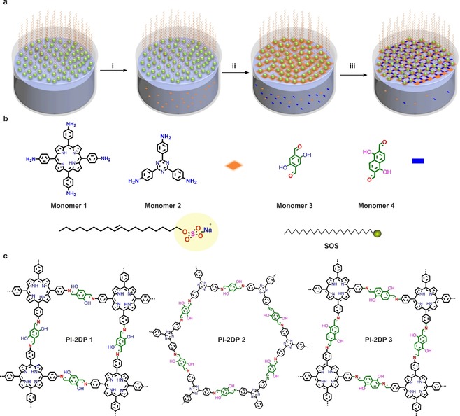
a) Schematic illustration of the synthesis of PI‐2DP at the air–water interface using SMAIS method. (i) Assembly of surfactant monolayer on the water surface. (ii) Pre‐organization of Monomer 1 underneath the surfactant monolayer. (iii) Polymerization at the surfactant–water interface. b) Chemical structures of monomers 1, 2, 3 and 4. c) Chemical structures of all synthetic PI‐2DPs.
Results and Discussion
Synthesis of PI‐2DP Film: Figure 1 a illustrates the interfacial synthesis procedures of PI‐2DP film. A chloroform solution of SOS was first spread at the air–water interface. With the evaporation of chloroform, the SOS molecules self‐assembled into a monolayer with SO4 − polar head groups toward the water phase (I). Then an aqueous solution of monomer 1 or 2 (5, 10, 15, 20‐tetrakis (4‐aminophenyl) porphyrin or tris (4‐aminophenyl) triazine, 0.7 μmole) protonated by hydrogen chloride was injected into the water phase (Figure 1 a, II) at 50 °C. Due to hydrogen bonding and electrostatic interactions, the protonated monomers could be readily adsorbed underneath the SOS monolayer. In the next step, monomer 3 or 4 (2, 5‐dihydroxyterephthalaldehyde or 1,5‐dihydroxynaphthalene‐2,6‐dicarbaldehyde, 2.8 μmole) was added to the water phase and diffused to the interface where polymerization was triggered with the formation of imine bonds between amine and aldehyde groups (Figure 1 a, III). The interfacial reaction was kept at 50 °C for 5 days to provide a highly crystalline PI‐2DP film. The synthetic PI‐2DP films exhibited a large area with lateral size up to several cm2 on the water surface. After horizontal transfer, the films could even cover 4‐inch SiO2/Si wafer without any noticeable defects and wrinkles (Figure 2 a). The atomic force microscopy (AFM) measurements revealed the thickness of obtained PI‐2DP films as ≈70 nm (PI‐2DP 1), ≈65 nm (PI‐2DP 2) and ≈40 nm (PI‐2DP 3), respectively (Figure 2 a and Figure S1). Moreover, the SMAIS strategy provided the possibility to control the thickness of PI‐2DP films just by varying the monomer concentration. For instance, the thickness of PI‐2DP 1 film could be tuned from 6 to 200 nm by varying the concentration of monomer 1 from 0.2 μm to 2.7 μm and monomer 2 from 1.19 μm to 11.7 μm (Figure 2 c). Furthermore, Raman spectroscopy was performed to gain insight into the chemical composition of PI‐2DP films (Figure 2 e). The Raman spectra show the disappearance of characteristic aldehyde C=O stretch peak at 1675 cm−1 for monomer 3 in PI‐2DP films and the emergence of a new peak for (‐C=N‐) (1650 cm−1; PI‐2DP 1, PI‐2DP 2 and PI‐2DP 3), demonstrating that aldehyde monomers were efficiently transformed into imine polymers in PI‐2DP films.19
Figure 2.
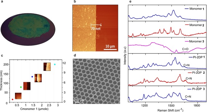
a) Photographic image of PI‐2DP 1 on 4‐inch 300 nm SiO2/Si wafer. b) AFM image of PI‐2DP 1 on 300 nm SiO2/Si wafer. c) The thickness of PI‐2DP 1 with respect to concentration of precursor monomer 1 and 3. (Inset: AFM images of PI‐2DP 1 on 300 nm SiO2/Si wafer). d) SEM image of free‐standing PI‐2DP 1 synthesized at 50 °C and suspended over hexagonal copper mesh grid. e) Raman spectra of precursor monomers and PI‐2DP films.
Structural Characterization of PI‐2DP Film: To investigate the crystallinity and molecular structures of the three PI‐2DPs, we conducted high‐resolution transition electron microscopy (HRTEM) and selected area electron diffraction (SAED) measurements. Towards this end, PI‐2DP films were horizontally transferred onto a hexagonal copper mesh with a hole size of 20 μm, on which they remained free‐standing with only a few cracks visible which are likely induced by drying/transfer process (Figure 2 d and Figure S1). Subsequent HRTEM imaging illustrates clearly the square lattice of PI‐2DP 1 and 3, as well as the hexagonal lattice of PI‐2DP 2 (Figure 3 a–c). As shown in the SAED pattern (insets in Figure 3 a–c), the nearest reflections at 0.40 nm−1 (PI‐2DP 1), 0.31 nm−1 (PI‐2DP 2), and 0.35 nm−1 (PI‐2DP 3) correspond to interplanar spacing of 2.50 nm, 3.22 nm, and 2.85 nm, respectively (Figure S2). The lattice symmetry and parameters determined from the HRTEM images and SAED patterns agree well with the atomic models derived by density functional theory (DFT) calculations (Table S1). Remarkably, the developed PI‐2DP films are highly crystalline without any amorphous fragments (Figure S3), demonstrating the versatility and generality of the SMAIS method for the dynamic imine chemistry, which are even superior to our recently reported 2D polyimide and 2D polyamide films where about 40 % amorphous areas were identified. Note that the control experiment without using surfactant failed to yield densely‐packed crystalline PI‐2DP films. The resultant PI‐2DP films were dominated by largely occupied amorphous regions (Figure S4).
Figure 3.
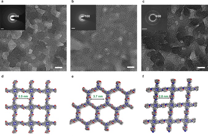
a) TEM images and SAED patterns (inset) of PI‐2DP films synthesized at 50 °C: a) PI‐2DP 1, b) PI‐2DP 2 c) PI‐2DP 3. Scale bar: 20 nm. The inset images are the relevant SAED patterns. Scale bar: 0.5 nm−1. d–f) Calculated DFT structures of PI‐2DP 1, PI‐2DP 2 and PI‐2DP 3, respectively. Grey: carbon; blue: nitrogen; red: oxygen; white: hydrogen.
To further characterize the role of the surfactant monolayer, we investigated the self‐assembly of porphyrin monomer 1 under the surfactant monolayer. The interfacial reaction was carried out by the identical conditions but without the addition of monomer 2. Due to hydrogen bonding and electrostatic interactions between protonated monomer 1 and SO4 − head groups of SOS, monomer 1 could be readily adsorbed underneath the SOS monolayer, leading to a local pre‐organization of monomer 1 with a face‐on configuration. As shown in Figure S5, the co‐assembled film of monomer 1 and SOS presented an ordered network structure comprising repeated square units with a size of 15.0 Å. Notably, the lattice spacing is in perfect agreement with that of the porphyrin self‐assembly in 2D plane. These results suggest that a face‐on adsorption of monomer 1 beneath the surfactant monolayer confines the subsequent polymerization reaction within the interfacial plane (i.e., 2D confinement).
Analysis of Nucleation and 2D Polymer Crystal Formation Process: To gain insight into the formation mechanism of the highly polycrystalline PI‐2DP film, we probed the crystal growth process using time‐dependent TEM imaging. The classical nucleation process of organic crystal follows a two‐step process which involves densification of monomers in the amorphous state followed by the nucleation of crystallites.20 In other case, monomers polymerize into oligomers where they nucleate either through stacking or through monomer addition onto the template structure.21 Our strategy follows the later one, where the crystallite nucleates through the addition of monomer onto the surfactant monolayer at the air–water interface.
We took highly crystalline PI‐2DP 1 as an example to study the detailed elucidation of nucleation and crystal formation process. Figure 4 shows the snapshots of the PI‐2DP 1 formation after 1, 3 and 5 days at 50 °C. After 1 day, small crystallites started to emerge at the air–water interface. Interestingly, despite the 2D confinement, the in‐plane rotation of the crystallites was not prohibited, leading to the formation of domains with random in‐plane orientations. At this stage, some amorphous fragments coexisted with the crystallites, which can be attributed to the stochastically adsorbed monomers beneath the SOS monolayer. As the reaction proceeded to 3 days, the crystallites expanded laterally and neighboring crystalline domains began to coalesce. As shown in Figure 4 c, we noticed an inhomogeneity in image contrast; the larger grains exhibit darker contrast. Assuming that the growth rate does not vary significantly from domain to domain, then the larger domains should have been formed earlier than the smaller ones. This result also suggests a temporal overlap between nucleation and growth. The lateral expansion of the crystalline domains continued until the surface coverage approached saturation, giving rise to a highly polycrystalline film without any amorphous residuals (Figure 4 d, 5 days). Strikingly, we did not observe any overlap between the crystalline domains. This result suggests a strong lock‐in effect along the stacking direction, which reveals that the stacking of two misoriented layers is energetically unfavorable. In addition, upon coalescence, the grains merely “collided” with each other, whereas no sign of Ostwald‐ripening has been observed despite the high reversibility of imine‐linkage.
Figure 4.
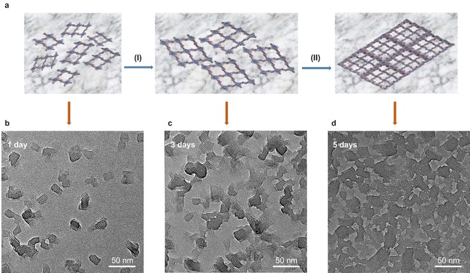
a) Schematic representation of the growth of PI‐2DP 1 at the interfaces with time. Time‐dependent TEM images of PI‐2DP 1 synthesized at 50 °C after 1 day (b), 3 days (c), and 5 days (d).
Next, we unraveled the effect of reaction temperature on the polymerization rate and crystallinity of PI‐2DP film. Figure S6 presents the TEM images of densely packed polycrystalline structures of PI‐2DP 1 films synthesized at 25 °C and 1 °C, respectively. Compared with that at 50 °C, the single‐crystalline domains with square symmetry are randomly oriented and the average domain size in all the cases (25 °C, 1 °C and 50 °C) are up to approx. 50 nm, which suggests the insignificant influence of temperature on domain size. Time‐dependent TEM measurements were performed on PI‐2DP 1 synthesized at 1 °C and 25 °C. These control experiments generated similar results in terms of growth mechanism (Figure S7) with that at 50 °C. Due to the different diffusion rate of monomers at varied temperature,22 longer reaction times (7–12 days) were required to yield densely packed polycrystalline film at lower temperature. Therefore, the control experiments suggest that reaction temperature plays a vital role in the 2D polymer crystal formation rate, whereas its impact on crystalline domain size is insignificant.
Lewis Acid Catalyst Mediated Synthesis of PI‐2DP: Besides the reaction temperature, catalysts play a crucial role in the rate‐limiting step of converting amorphous imine polymer network into crystalline framework.23 Thereby, a small amount of Lewis acid metal triflate catalyst Yb(OTf)3 was added into the water phase. The subsequent interfacial polymerization at 50 °C yielded a PI‐2DP 1 film with a substantial increase in average crystalline domain size up to ≈150 nm (Figure 5 a), which is larger than that with acetic acid as catalyst (Figure S8) and without catalyst (Figure S6). Here, water‐tolerant Yb(OTf)3 can efficiently catalyze imine formation and transamination reaction,24 thus enabling the enhancement of the crystallinity of 2D polyimine.13 SAED performed on a single‐crystalline domain (Figure 5 b) displays a square diffraction pattern with nearest reflections at 0.4 nm−1 (i.e., a=b=2.5 nm, γ=90°). Notably, the employment of Yb(OTf)3 catalyst led to reduced lattice distortion, which was evidenced by the appearance of hk0 reflections (h, k=1, 2, 3…) in the SAED pattern (Figure 5 b) as well as HRTEM imaging (Figure 5 e). Synchrotron grazing‐incidence wide‐angle X‐ray scattering (GIWAXS) measurement was performed to elucidate the molecular packing of PI‐2DP 1 on a macroscopic scale. The reflection peaks of PI‐2DP 1 at Qxy=0.23 Å−1, 0.33 Å−1, 0.48 Å−1 and 0.73 Å−1 were observed (Figure 5 c,d), which correspond to (0,1,0), (1,−1,1), (0,2,0), (1,−3,0) interlayer planes, respectively. The resultant unit cell was assigned with a=27 Å, b=27 Å, γ=88.9°, and the interlayer spacing was 3.9 Å, agreeing well with the SAED results and DFT calculation (Table S1). The large crystalline domains of PI‐2DP 1 with significantly reduced distortion enabled us to visualize the molecular structure by AC‐HRTEM. Figure 5 e presents the HRTEM image of PI‐2DP 1 showing the square lattice with 25.0 Å spacing. As demonstrated by image simulation (inset image in Figure 5 e), the porphyrin units appear bright on a dark background, allowing us to determine the domain boundary structure with molecular precision (Figure S10 and Figure S11).
Figure 5.
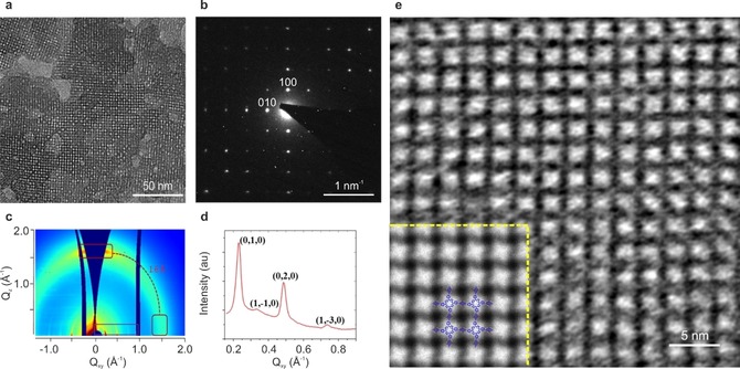
a) TEM image showing the increased average domain size up to ≈150 nm. b) SAED pattern of a single‐crystalline domain along the [001] direction of PI‐2DP 1. c) GIWAXS image of PI‐2DP 1 on 300 nm SiO2/Si. d) In plane projection of GIWAXS data from (c). e) HRTEM image showing the square lattice with significantly reduced distortion (Inset: simulated HRTEM image with the atomic model overlaid, the porphyrin units appear bright, Figures S9 and S10).
Optical and Electronic Properties: The optical and electronic properties of PI‐2DP 1 were investigated by UV‐vis absorption spectroscopy and ultraviolet photoelectron spectroscopy (UPS). Figure 6 a shows the absorption spectra of the samples, revealing the Soret (S) and Q bands of monomer 1 and PI‐2DP 1. The S band of PI‐2DP 1 is red‐shifted by ≈40 nm and broader when compared with that of the monomer 1. This bathochromic shift is a consequence of the conjugated configuration of PI‐2DP 1, enabling the formation of extended π system in PI‐2DP 1. From the data, an optical band gap inferred from the Q band of the absorbance spectra of PI‐2DP 1 was estimated as ≈1.4 eV which agrees with the electronic band gap of 1.38 eV obtained from DFT calculations (Figure S12). UPS measurements were obtained using a HeIα excitation source at 21.22 eV while recording the kinetic energies of the photoelectrons by a hemispherical analyzer (Specs Phoibos 100). Figure 6 b shows the UPS spectrum of a PI‐2DP 1 film on top of a gold substrate. The work function (Wf) can be extracted from the high binding energy cutoff position (E co) and shows a value of Wf=4.22 eV. The inset displays an enhanced section of the occupied density of states close to the Fermi level, from which the onset of the HOMO level valence band vs. the Fermi level can be extracted. The resulting energy level diagram is shown in Figure 6 c as well. The low ionization energy value of 5.38 eV in combination with the previously discussed band gap of 1.4 eV is indicative of a delocalized π‐electron system, achieved through the conjugation in PI‐2DP 1 film. The low IE value of 5.38 eV makes PI‐2DP 1 a promising candidate as hole injection or hole transport material in organic optoelectronic devices.
Figure 6.
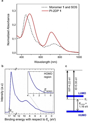
a) UV‐vis spectra of PI‐2DP 1 and monomer 1‐SOS film. b) UPS measurement of PI‐2DP 1 (inset: enhanced HOMO region). c) Energy level diagram of PI‐2DP 1.
Photoconductivity by Terahertz Spectroscopy: Terahertz (THz) spectroscopy has been demonstrated as a powerful non‐contact method for time‐resolving photoconductivity properties of semiconductors.25 The intrinsic charge transport properties of PI‐2DP 1 was evaluated by THz spectroscopy. A thin PI‐2DP 1 film with the thickness of 20 nm and an averaged domain size of ≈150 nm was placed onto a 1 mm‐thick fused silica substrate. THz spectroscopy was performed in transmission mode by employing 400 nm pump, 50 fs pulsewidth and 1 KHz repetition rate (90 uJ cm−2). After an ultrafast laser pulse excites the material optically, electron‐hole pairs are generated. The photoconductivity induced in the sample is then probed over a 0.4–2 THz frequency range. Figure 7 a presents the time‐resolved transient signal of the real component of the conductivity which is characterized by an ultra‐fast rise followed by a decay of approximately 1 ps. This response is consistent with the generation of quasi‐free electron‐hole pairs that subsequently condense into localized states. To obtain the mobility of PI‐2DP 1 film, we determine the frequency‐resolved conductivity over the frequency range of 0.4–2 THz. The real and imaginary conductivity components as a function of frequency (0.3 ps after pump excitation) are plotted in Figure 7 b. The obtained spectrum can be described by the phenomenological Drude–Smith model, which allows to evaluate the transient mobility of 0.01 cm2 V−1 s−1 (the details seen in SI). This mobility represents a lower bound estimate as we assumed that all photons are absorbed and generate quasi‐free charges immediately after pump excitation.
Figure 7.
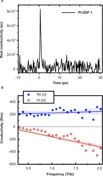
a) THz characterization of PI‐2DP 1. The conductivity of PI‐2DP 1 as a function of the pump–probe delay (excitation wavelength, 400 nm, 90 μJ cm−2). b) Frequency‐resolved complex‐value of PI‐2DP 1 (1 ps after photoexcitation). Blue filled circles and transparent blue circles represent the measured real and imaginary components, respectively, and lines through the data points represent best fit obtained using the Drude–Smith model.
As contrast, amorphous PI‐2DP 1 film (Figure S4) synthesized without surfactant on the water surface failed to generate a photo conductivity during the THz spectroscopy measurements. These results suggest that long range ordered structures are essential to enhance charge transport in 2D polyimine films. It should be emphasized that the mobility value in crystalline PI‐2DP 1 is superior to the previously reported polyimine films and even higher than sulfur‐enriched conjugated polymer nanosheets (2DP‐S)26 and azulene‐bridged coordination polymer films (PiCBA).27
Conclusion
In summary, we have demonstrated a successful synthesis of three crystalline imine‐based 2D polymer films with square and hexagonal patterns via SMAIS method, respectively. The achieved PI‐2DPs are freestanding with lateral dimensions in the range of cm2. With the assistance of Lewis acid metal triflate as catalyst, the average single‐crystalline domain size of the obtained PI‐2DP 1 film can reach ≈150 nm. The crystal formation mechanism was investigated with the support of time‐dependent TEM observation, which reveals a crystallite nucleation‐ coalescence progress. The abundance of large crystalline domains provides a perfect architecture to investigate the intrinsic charge transport properties of PI‐2DP films. The synthetic PI‐2DP 1 exhibits a transient mobility as high as 0.01 cm2 V−1 s−1 as characterized by THz spectroscopy. Our work highlights to utilize dynamic covalent chemistry and SMAIS strategy towards the highly crystalline large‐area 2D polymer films and further establish the structure‐transport property relationship which is a significant step for the development of organic 2D materials as well as their future device integration for electronics, sensor, separation as well as energy conversion and storage. How to control the interfacial polymerization conditions, such as nucleation density, surfactant types, monomer design and reaction catalysts, for growing larger crystalline domains and even single crystals remains a formidable task and thus requires further research.
Conflict of interest
The authors declare no conflict of interest.
Supporting information
As a service to our authors and readers, this journal provides supporting information supplied by the authors. Such materials are peer reviewed and may be re‐organized for online delivery, but are not copy‐edited or typeset. Technical support issues arising from supporting information (other than missing files) should be addressed to the authors.
Supplementary
Acknowledgements
This work was financially supported by ERC Grant on T2DCP, ERC Starting Grant (FC2DMOF, No. 852909), EU Graphene Flagship and COORNET (SPP 1928) as well as the German Science Council, Centre of Advancing Electronics Dresden, EXC1056, (cfaed) and OR 349/1. H.Q. and U.K. thank the financial support by the DFG in the framework of the “SALVE” (Sub‐Angstrom Low‐Voltage Electron Microscopy) project as well the Ministry of Science, Research and the Arts (MWK) of Baden‐Wuerttemberg in the framework of the SALVE project. Z.K. thanks financial support from the National Natural Science Foundation of China (51873236). We thank Dresden Center for Nanoanalysis (DCN) at TUD and Dr. Petr Formanek (Leibniz Institute for Polymer Research, IPF, Dresden) and Christine Damm (IFW) for the use of facilities. GIWAXS was carried out at DESY, a member of the Helmholtz Association (HGF), and at Helmholtz‐Zentrum Berlin. We would like to thank M. Schwartzkopf for assistance (P03‐MINAXS beamline) and Dr. Daniel Többens (KMC‐2 beamline). We thank HGF and HZB for the allocation of neutron/synchrotron radiation beamtime and ZIH Dresden for computer time.
H. Sahabudeen, H. Qi, M. Ballabio, M. Položij, S. Olthof, R. Shivhare, Y. Jing, S. Park, K. Liu, T. Zhang, J. Ma, B. Rellinghaus, S. Mannsfeld, T. Heine, M. Bonn, E. Cánovas, Z. Zheng, U. Kaiser, R. Dong, X. Feng, Angew. Chem. Int. Ed. 2020, 59, 6028.
Contributor Information
Prof. Dr. Zhikun Zheng, Email: zhengzhikun@mail.sysu.edu.cn.
Prof. Dr. Ute Kaiser, Email: ute.kaiser@uni-ulm.de.
Dr. Renhao Dong, Email: renhao.dong@tu-dresden.de.
Prof. Dr. Xinliang Feng, Email: xinliang.feng@tu-dresden.de.
References
- 1.
- 1a. Segura J. L., Mancheño M. J., Zamora F., Chem. Soc. Rev. 2016, 45, 5635–5671; [DOI] [PubMed] [Google Scholar]
- 1b. Huang N., Wang P., Jiang D., Nat. Rev. Mater. 2016, 1, 16068; [Google Scholar]
- 1c. Kandambeth S., Dey K., Banerjee R., J. Am. Chem. Soc. 2019, 141, 1807–1822; [DOI] [PubMed] [Google Scholar]
- 1d. DeBlase C. R., Dichtel W. R., Macromolecules 2016, 49, 5297–5305. [Google Scholar]
- 2. Kandambeth S., Shinde D. B., Panda M. K., Lukose B., Heine T., Banerjee R., Angew. Chem. Int. Ed. 2013, 52, 13052–13056; [DOI] [PubMed] [Google Scholar]; Angew. Chem. 2013, 125, 13290–13294. [Google Scholar]
- 3. Dalapati S., Addicoat M., Jin S., Sakurai T., Gao J., Xu H., Irle S., Seki S., Jiang D., Nat. Commun. 2015, 6, 7786. [DOI] [PMC free article] [PubMed] [Google Scholar]
- 4. Ma T., Kapustin E. A., Yin S. X., Liang L., Zhou Z., Niu J., Li L.-H., Wang Y., Su J., Li J., et al., Science 2018, 361, 48–52. [DOI] [PubMed] [Google Scholar]
- 5. Rabbani M. G., Sekizkardes A. K., Kahveci Z., Reich T. E., Ding R., El-Kaderi H. M., Chem. Eur. J. 2013, 19, 3324–3328. [DOI] [PubMed] [Google Scholar]
- 6. Fan H., Gu J., Meng H., Knebel A., Caro J., Angew. Chem. Int. Ed. 2018, 57, 4083–4087; [DOI] [PubMed] [Google Scholar]; Angew. Chem. 2018, 130, 4147–4151. [Google Scholar]
- 7. Wan S., Gándara F., Asano A., Furukawa H., Saeki A., Dey S. K., Liao L., Ambrogio M. W., Botros Y. Y., Duan X., et al., Chem. Mater. 2011, 23, 4094–4097. [Google Scholar]
- 8. Xu H., Tao S., Jiang D., Nat. Mater. 2016, 15, 722–726. [DOI] [PubMed] [Google Scholar]
- 9. Li Z., Huang N., Lee K. H., Feng Y., Tao S., Jiang Q., Nagao Y., Irle S., Jiang D., J. Am. Chem. Soc. 2018, 140, 12374–12377. [DOI] [PubMed] [Google Scholar]
- 10. Lin C.-Y., Zhang D., Zhao Z., Xia Z., Adv. Mater. 2018, 30, 1703646. [DOI] [PubMed] [Google Scholar]
- 11.
- 11a. Feng X., Schlüter A. D., Angew. Chem. Int. Ed. 2018, 57, 13748–13763; [DOI] [PubMed] [Google Scholar]; Angew. Chem. 2018, 130, 13942–13959; [Google Scholar]
- 11b. Wang L., Sahabudeen H., Zhang T., Dong R., npj. 2D Mater. Appl. 2018, 2, 26; [Google Scholar]
- 11c. Dong R., Zhang T., Feng X., Chem. Rev. 2018, 118, 6189–6235. [DOI] [PubMed] [Google Scholar]
- 12. Dey K., Pal M., Rout K. C., Kunjattu H S., Das A., Mukherjee R., Kharul U. K., Banerjee R., J. Am. Chem. Soc. 2017, 139, 13083–13091. [DOI] [PubMed] [Google Scholar]
- 13. Matsumoto M., Valentino L., Stiehl G. M., Balch H. B., Corcos A. R., Wang F., Ralph D. C., Mariñas B. J., Dichtel W. R., Chem 2018, 4, 308–317. [Google Scholar]
- 14.
- 14a. Sahabudeen H., Qi H., Glatz B. A., Tranca D., Dong R., Hou Y., Zhang T., Kuttner C., Lehnert T., Seifert G., et al., Nat. Commun. 2016, 7, 13461; [DOI] [PMC free article] [PubMed] [Google Scholar]
- 14b. Müller V., Hinaut A., Moradi M., Baljozovic M., Jung T. A., Shahgaldian P., Möhwald H., Hofer G., Kröger M., King B. T., et al., Angew. Chem. Int. Ed. 2018, 57, 10584–10588; [DOI] [PubMed] [Google Scholar]; Angew. Chem. 2018, 130, 10744–10748; [Google Scholar]
- 14c. Wang W., Shao F., Kröger M., Zenobi R., Schlüter A. D., J. Am. Chem. Soc. 2019, 141, 9867–9871. [DOI] [PubMed] [Google Scholar]
- 15. Feldblyum J. I., McCreery C. H., Andrews S. C., Kurosawa T., Santos E. J. G., Duong V., Fang L., Ayzner A. L., Bao Z., Chem. Commun. 2015, 51, 13894–13897. [DOI] [PubMed] [Google Scholar]
- 16.
- 16a. Cai S.-L., Zhang Y.-B., Pun A. B., He B., Yang J., Toma F. M., Sharp I. D., Yaghi O. M., Fan J., Zheng S.-R., et al., Chem. Sci. 2014, 5, 4693–4700; [Google Scholar]
- 16b. Medina D. D., Petrus M. L., Jumabekov A. N., Margraf J. T., Weinberger S., Rotter J. M., Clark T., Bein T., ACS Nano 2017, 11, 2706–2713; [DOI] [PMC free article] [PubMed] [Google Scholar]
- 16c. Medina D. D., Werner V., Auras F., Tautz R., Dogru M., Schuster J., Linke S., Döblinger M., Feldmann J., Knochel P., et al., ACS Nano 2014, 8, 4042–4052; [DOI] [PMC free article] [PubMed] [Google Scholar]
- 16d. Joshi T., Chen C., Li H., Diercks C. S., Wang G., Waller P. J., Li H., Bredas J., Yaghi O. M., Crommie M. F., Adv. Mater. 2019, 31, 1805941. [DOI] [PubMed] [Google Scholar]
- 17. Liu K., Qi H., Dong R., Shivhare R., Addicoat M., Zhang T., Sahabudeen H., Heine T., Mannsfeld S., Kaiser U., et al., Nat. Chem. 2019, 11, 994–1000. [DOI] [PubMed] [Google Scholar]
- 18. Zhang T., Qi H., Liao Z., Horev Y. D., Panes-Ruiz L. A., Petkov P. S., Zhang Z., Shivhare R., Zhang P., Liu K., et al., Nat. Commun 2019, 10, 4225. [DOI] [PMC free article] [PubMed] [Google Scholar]
- 19. Dai W., Shao F., Szczerbiński J., McCaffrey R., Zenobi R., Jin Y., Schlüter A. D., Zhang W., Angew. Chem. Int. Ed. 2016, 55, 213–217; [DOI] [PubMed] [Google Scholar]; Angew. Chem. 2016, 128, 221–225. [Google Scholar]
- 20. Shibata O., Nakahara H., Moroi Y., J. Oleo Sci. 2015, 64, 1–8. [DOI] [PubMed] [Google Scholar]
- 21.
- 21a. Li H., Chavez A. D., Li H., Li H., Dichtel W. R., Bredas J.-L., J. Am. Chem. Soc. 2017, 139, 16310–16318; [DOI] [PubMed] [Google Scholar]
- 21b. Koo B. T., Heden R. F., Clancy P., Phys. Chem. 2017, 19, 9745–9754. [DOI] [PubMed] [Google Scholar]
- 22.
- 22a. Ángeles Fontecha-Cámara M., López-Ramón M. V., Álvarez-Merino M. A., Moreno-Castilla C., Langmuir 2006, 22, 9586–9590; [DOI] [PubMed] [Google Scholar]
- 22b. Schreiber B., Brinkmann T., Schmalz V., Worch E., Water Res. 2005, 39, 3449–3456; [DOI] [PubMed] [Google Scholar]
- 22c. Manchanda P., Chisca S., Upadhyaya L., Musteata V.-E., Carrington M., Nunes S. P., J. Mater. Chem. 2019, 7, 25802–25807. [Google Scholar]
- 23. Matsumoto M., Dasari R. R., Ji W., Feriante C. H., Parker T. C., Marder S. R., Dichtel W. R., J. Am. Chem. Soc. 2017, 139, 4999–5002. [DOI] [PubMed] [Google Scholar]
- 24.
- 24a. Kobayashi S., Sugiura M., Kitagawa H., Lam W. W.-L., Chem. Rev. 2002, 102, 2227–2302; [DOI] [PubMed] [Google Scholar]
- 24b. Giuseppone N., Schmitt J.-L., Lehn J.-M., Angew. Chem. Int. Ed. 2004, 43, 4902–4906; [DOI] [PubMed] [Google Scholar]; Angew. Chem. 2004, 116, 5010–5014; [Google Scholar]
- 24c. Ciaccia M., Stefano S. D., Org. Biomol. Chem. 2015, 13, 646–654. [DOI] [PubMed] [Google Scholar]
- 25. Dong R., Han P., Arora H., Ballabio M., Karakus M., Zhang Z., Shekhar C., Adler P., Petkov P. S., Erbe A., et al., Nat. Mater. 2018, 17, 1027–1032. [DOI] [PubMed] [Google Scholar]
- 26. Su Y., Yao Z., Zhang F., Wang H., Mics Z., Cánovas E., Bonn M., Zhuang X., Feng X., Adv. Funct. Mater. 2016, 26, 5893–5902. [Google Scholar]
- 27. Yang C., Schellhammer K. S., Ortmann F., Sun S., Dong R., Karakus M., Mics Z., Löffler M., Zhang F., Zhuang X., et al., Angew. Chem. Int. Ed. 2017, 56, 3920–3924; [DOI] [PubMed] [Google Scholar]; Angew. Chem. 2017, 129, 3978–3982. [Google Scholar]
Associated Data
This section collects any data citations, data availability statements, or supplementary materials included in this article.
Supplementary Materials
As a service to our authors and readers, this journal provides supporting information supplied by the authors. Such materials are peer reviewed and may be re‐organized for online delivery, but are not copy‐edited or typeset. Technical support issues arising from supporting information (other than missing files) should be addressed to the authors.
Supplementary


