Abstract
A hallmark of quantum control is the ability to manipulate quantum emission at the nanoscale. Through scanning tunneling microscopy-induced luminescence (STML), we are able to generate plasmonic light originating from inelastic tunneling processes that occur in the vacuum between a tip and a few-nanometer-thick molecular film of C60 deposited on Ag(111). Single photon emission, not of molecular excitonic origin, occurs with a 1/e recovery time of a tenth of a nanosecond or less, as shown through Hanbury Brown and Twiss photon intensity interferometry. Tight-binding calculations of the electronic structure for the combined tip and Ag–C60 system results in good agreement with experiment. The tunneling happens through electric-field-induced split-off states below the C60 LUMO band, which leads to a Coulomb blockade effect and single photon emission. The use of split-off states is shown to be a general technique that has special relevance for narrowband materials with a large bandgap.
Keywords: scanning tunneling microscopy-induced luminescence, plasmon, antibunching, Coulomb blockade, split-off states
Discrete electronic states split-off from Bloch bands have been of interest for decades1 and continue to be at the forefront of solid-state research and development because of their intimate connection with point defects in materials, such as dopant atoms and color centers, which exhibit nonclassical effects such as single photon emission. Their optoelectronic properties are well-described by solving the Schrödinger equation for a periodic potential with a local perturbation, with the perturbation depending on the material composition of the defect. Thus, exploring different ways to create and manipulate split-off states are necessary in order to gain tunability beyond this materiality constraint.2−4 Efforts in this direction include quantum dot nanostructures,5,6 but their optoelectronic properties depend on single exciton (electron–hole pair) decay7 that is not easily modifiable.8
Thus, a concrete demonstration that single photon emission can be achieved without relying on internal molecular or quantum dot transitions is in order. To this end, we observe that the very origin of split-off states, the local perturbation, need not be materials based and, in fact, can also be an external perturbation. This motivates using a nanometer tip of a scanning tunneling microscope (STM) as a local perturbation, in a system that can spotlight the principle of single photon emission in a more materials-independent manner.
As a proxy for a generic semiconductor on a metallic substrate, we use a thin C60 slab that couples weakly to a Ag(111) substrate which itself was chosen because it has strong plasmonic resonances in the visible range. C60 has the advantage that its electronic structure is accurately represented by a simple model,9 which enables us to rationalize the agreement we obtained between theory and experiment. The narrowness of the C60 bands enables creating split-off states with the electric field10 induced by applying a sufficient bias voltage across the tip–sample tunnel junction.11 In analogy to having a point defect at the tip position, the split-off states tend to be approximately localized on the C60 molecule directly beneath the tip, leading to a strong Coulomb repulsion. This leads to a Coulomb blockade of tunneling events whereby electrons are forced to tunnel one at a time. Consequently, the photon emission via tip-induced plasmons also occurs one at a time12 whenever it results from tunneling via such states.13
This phenomenon provides an additional handle over single photon emission in a STM setting because it involves electrons tunneling inelastically through a field-induced split-off state. Whether or not split-off states are formed below the Fermi energy of the sample, EFS, is directly controllable by the bias voltage and is manifestly shown in our measurements (see also Supporting Figure 4).
Controlling the inelastic tunneling is easier than controlling the formation of excitons. Thus, the performance of this tip-induced quantum dot and single photon emitter in terms of recovery time, without any optimization, is already competitive with epitaxial quantum dot emitters.14 This work highlights the important role of local electric fields in probe microscopies,15 expands the variety of quantum states that can be made with C6016 and, indeed, demonstrates the general significance of field-induced split-off states.
Results and Discussion
The experiments are performed with an STM with optical access, shown schematically in Figure 1. A voltage bias is applied across the junction formed between the tip and the Ag(111) substrate covered by C60 in the form of a few-monolayer (ML) thick film, with regions that are 4–5 ML thick.17 The tunnel current is kept constant by a feedback loop, and the light originating from tunneling processes is characterized. Its intensity correlation function g(2)(t) is measured with a photon intensity interferometer in a Hanbury Brown and Twiss configuration,18 and its optical spectrum is analyzed in a spectrograph.19
Figure 1.
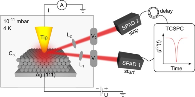
A scanning tunneling microscope combined with a Hanbury Brown and Twiss interferometer. Light radiating from a junction formed between a Au tip and multilayer C60-Ag(111) substrate travels along optical paths (1, 2) containing (L)enses and (V)iewports to a pair of single-photon avalanche detectors (SPADs). The number of photon coincidence events as a function of time delay t between pulses from the SPADs, g(2)(t), is measured with a time-correlated single-photon counter (TCSPC). The voltage bias (U) is applied to the substrate. The tunnel current (I) is measured with a picoammeter (A). A third optical path to an optical spectrometer is not shown.
The electronic structure of the system is studied theoretically using a tight-binding model of the five HOMO (Hu) and three LUMO (T1u) states on each C60 molecule (see Supporting Information). The molecules are arranged in laterally infinite layers as a (111) surface, with each layer stacked in a face centered cubic structure identical to bulk C60, taking into account orientational ordering with four different orientations of the molecules in the unit cell.20 The potential from the tip is described by introducing image charges, satisfying the boundary conditions at the tip and the Ag(111)-C60 and C60-vacuum interfaces. The electronic structure is calculated in a Green’s function formalism, assuming that the tip potential affects only a few hundred molecules (see Supporting Information).
The light emission of molecular C60 thin films induced by scanning tunneling microscopy can be plasmonic (as in this work), excitonic,21 or a mixture22 of both. It is a strong function of tip, sample, and tunneling parameters. In this work, the tip–sample distance is in the neighborhood of 0.4 nm estimated from z-spectroscopy approach curves. Of interest in this study are regions of molecularly thick C60, free of emission centers,23,24 whose emission is purely plasmonic with no evidence for any excitonic contribution known to occur at the different types of defects reported earlier.17,21,22 Consequently, the light spectrum contains only broad plasmonic modes, such as the features seen at 2 and 1.8 eV in Figure 2a, excited by inelastic scattering events in the tunnel junction.22,23 This spectrum typically consists of several plasmon modes whose positions and intensities change substantially with tip shape and tip apex preparation. An energy level cartoon of the light emission process is shown in Figure 2b. Under the conditions allowing for light emission, tunneling occurs between metal sample and metal tip through a single electronic state split-off from the LUMO continuum. Note that this state is not due to a stationary defect in the C60 layer but induced by the electric field of the moveable STM tip.
Figure 2.
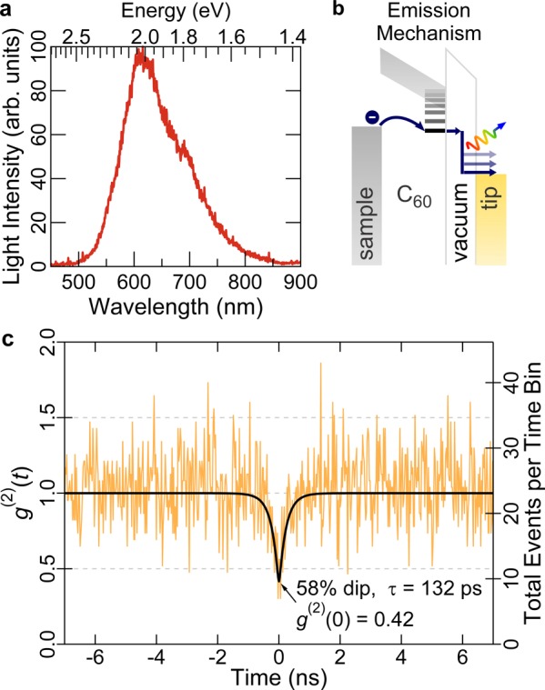
Plasmonic antibunching light emission from 5 ML C60 on Ag(111) measured at 125 pA, −3.5 V. (a) Spectrum measured on a C60 terrace, integration time 1200 s. (b) Cartoon of the tunneling through the lowest LUMO split-off state and light emission process. (c) Photon intensity correlation measured at the same position as in (a) immediately after, 7500 s accumulation time, 24.4 ps bin width. The black curve is a least-squares Poisson-weighted fit to the data, using a constant background, and the detector response convolved with a Laplace distribution, whose decay parameter τ is defined as the antibunching recovery time.
The g(2)(t) has a large correlation dip at t = 0 (Figure 2c) and satisfies g(2)(0) < g(2)(t) for all t > 0, unlike a typical plasmonic emission where g(2)(t) is unity (see Supporting Figure 2). Hence, the photon emission is antibunched. This is a statistical property of the light that cannot be discerned from the optical spectra alone and does not depend on the energetics of the plasmon modes in the spectra. Based on a 2-particle Hilbert space argument, its dip intensity of 58% (i.e., g(2)(0) = 0.42) is consistent with imperfect single photon emission of at most [1 – (1 – 2g(2))1/2]/g(2) = 1.42 photons on average.24 The antibunching recovery time is τ = 0.13 ns and reflects the tunneling of electrons from Ag(111) to the top C60 layer and not the average time interval between tunneling electrons, which is 1.3 ns for the 125 pA used in the measurement of Figure 2c. Note that the time constant of excitonic antibunching of emission centers on C60 under comparable tunneling conditions is 0.58 ns.21 An example of how this antibunching dip can be varied by changing either the tip–sample distance or bias voltage can be found in Supporting Figures 3 and 4. This work is a demonstration of antibunched plasmonic emission attained in an STM by circumventing the limitations set by emitter lifetimes, whether exciton-based25−27 or otherwise.28 The imperfectness of the emitter is later ascribed to two contributing mechanisms, the first involving only LUMO-derived states and the second involving both LUMO- and HOMO- derived states.
The photon statistics can be understood by analyzing the behavior of the electronic states. Figure 3a shows the topography of a C60 island. The cyan contours mark the terrace boundaries, with the labels indicating the terrace height in C60 layers. Figure 3b shows the integrated photon emission efficiency (light emission normalized by current) as a function of tip position. Figure 3c shows the relative tip position and photon emission efficiency along the magenta line in Figure 3a,b. Differential conductance (dI/dV) spectra shown in Figure 3d measured from the first to fifth terrace show a very pronounced peaked feature, present at the fourth and fifth terrace for this −3.5 V bias, 100 pA set point. Additional information for the sixth and seventh terrace can be found in the Supporting Figure 5. In all cases, the feature is particularly sharp, suggestive of a tunneling component through a single electronic state29 that is most clearly observable in experiments when it is near the HOMO band edge. It is not to be confused with a charge hysteresis in the system.30 We assigned it to a LUMO-derived state that has been pulled out of the LUMO continuum and below EFS by the electric field of the tip, based on theoretical calculations to follow. We emphasize that LUMO states typically appear at positive potentials, but can also appear at negative potentials under appropriate experimental conditions.17,31
Figure 3.
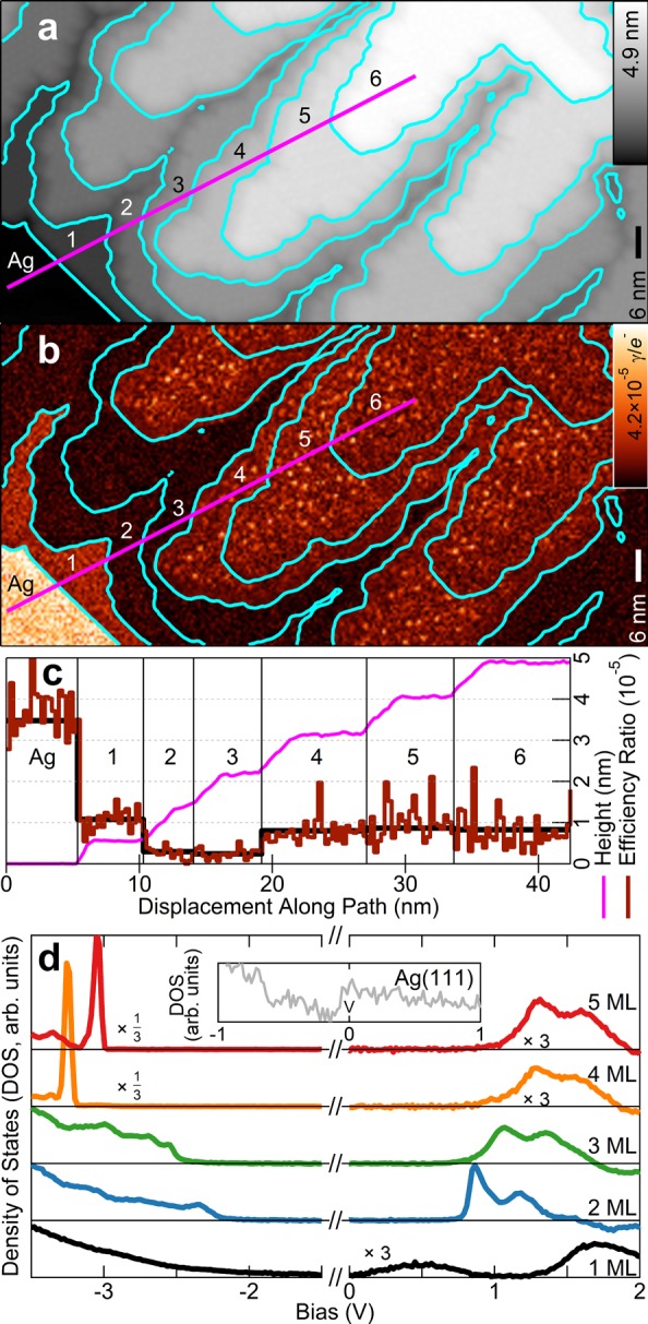
STML surface characterization of C60-Ag(111). (a) Topography of a C60 film on Ag(111); U = −3.5 V, I = 20 pA constant current. (b) Light emission map, where γ/e– denoting photons per electron, is calculated as light intensity × elementary charge unit/current; same set point as (a). (c) Line profiles of topography and emission efficiency along the magenta lines marked in (a) and (b), respectively. The thick black line follows the average efficiency value of each terrace. (d) Differential conductance (dI/dV) spectra of the substrate (inset) and of 1–5 ML C60 atop this substrate, with spectra shifted vertically for clarity; set point U = −3.5 V, I = 100 pA.
The controllability of the onset of light emission in the various C60 layers is of particular interest. Figure 4a shows the topography of one series of terraces from Figure 3. The thickness threshold at which luminescence occurs is lowered from the fourth to the second layer by changing the bias from −2.86 V to −4 V as seen in Figure 4b,c. This effect is examined further by measuring tunneling spectra on the fourth layer as a function of tip–sample distance. Figure 4d shows two peaked features later assigned to split-off states from the LUMO band. As the tip–sample distance is increased, the bias has to be made more negative to observe the peaked features32 (Figure 4e).
Figure 4.
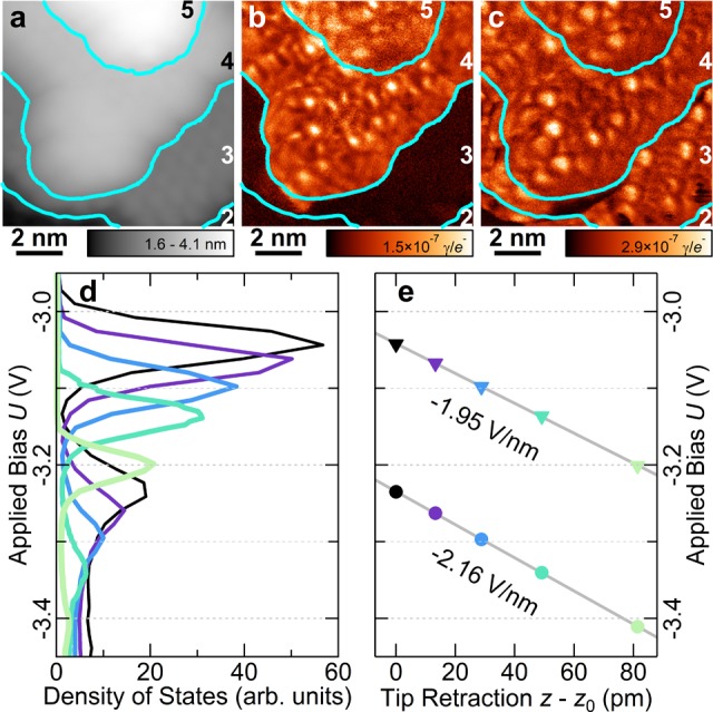
Controllability of resonant tunneling luminescence. Measurements of 2–5 MLs of C60 on Ag(111) at 100 pA constant current, with terrace boundary contours marked in cyan. (a, b) Topography and integrated photon emission efficiency, both at −2.86 V. Efficiency marked γ/e– denoting photons per electron is calculated as light intensity × elementary charge unit/current. (c) Integrated photon emission efficiency at −4.00 V. (d) Differential conductance (dI/dV) spectra on the fourth C60 terrace as a function of relative tip–sample distance. Two LUMO features are visible. (e) The energetic position of the LUMO features as a function of relative tip–sample distance. The lines are a fit to the data points and show that the LUMO features’ positions follow lines of constant electric field.
In this next step, we make comparisons with calculations. Consider four layers of C60 on an ideal metal surface substrate. Figure 5 shows the projected density of states (DOS) of the topmost layer. Now consider the LUMO states. It has band edges at 0.27 and 1.02 eV, with first moment 0.73 eV, and is concentrated between 0.4 and 1.0 eV, with a small tail extending to 0.27 eV. This tail is due to coupling to the innermost layer. Due to the strong image potential in the innermost layer, the DOS in this innermost layer extends down to 0.27 eV. Orbital mixing between the innermost layer and the topmost layer then leads to the DOS of the topmost layer to have a small tail that extends down to 0.27 eV as well. There is band bending due to the laterally periodic image potential in the substrate, but not due to the localized tip-induced potential. For instance, when a small bias of −0.68 V is applied to the tip, as in the black curve b of Figure 5, the band edges stay fixed, while the local DOS on the C60 directly below the tip is depleted at the upper band edge and accumulates at the lower edge. This causes the first moment to move to a lower potential, toward EFS, as seen by comparing the LUMO states of the green curve a and black curve b in Figure 5. This movement is due to the combined effects of the electrostatic and image potentials from the tip. (Details on the HOMO states of the same curves are available in Supporting Information.)
Figure 5.
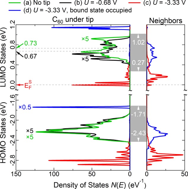
Calculated projected DOS of 4 ML C60-Ag(111) as a function of applied bias. Gray rectangles indicate the energy range and the onset values of the continuum band of C60 states. The band edges stay fixed and do not change with applied bias. Features beyond the band edge correspond to discrete split-off states. Sharp features overlapping with the continuum band are resonances. Arrows along the left vertical axis indicate the first moment of the bands.The corresponding theoretical band energies in the absence of hybridization are both 0.01 eV less. “Neighbors” denotes an average of the DOS of all six nearest-neighbor C60 molecules. All features are broadened with a fwhm Lorenzian of 0.02 eV. The green “no tip” curve is the projected DOS of the topmost layer.
For a critical applied voltage U, discrete split-off states appear below the LUMO band edge. This critical U exists because any state in a band is at most half a bandwidth in energy away from one band edge. Thus, a split-off state appears when the center of gravity of the DOS on the C60 below the tip has moved on the order of half the C60 LUMO bandwidth, depending on the details of the DOS. This effect is similar to split-off states caused by point impurities in semiconductors, and should not be confused with “band bending” in extended two-dimensional molecular layer systems nor thin layered materials that comprise van der Waals heterostructures. In contrast to the latter, the DOS is locally perturbed to the extent that it has little resemblance to the unperturbed DOS.
The split-off states in the red curve c of Figure 5 are localized on the C60 molecule below the tip with some extension to the neighboring molecules. The figure shows how the first of a series of LUMO split-off states is formed just below EFS for U = −3.33 V and four layers and allows tunneling to the tip through these states. The tunneling contribution from the first LUMO split-off state explains the sharp feature seen in Figure 3d for 4 and 5 ML C60. The details of the calculated LUMO DOS show that this LUMO-derived split-off state has most of its weight on the localized molecular orbitals on the C60 molecule below the tip, with some additional weight on neighboring molecules. Figure 4d shows the experimental behavior of the first and second split-off states in detail, which correspond to the calculated split-off states with most of their weight in the three LUMO states on the C60 molecule below the tip. Of the two split-off states, calculations reveal that the first has more weight because it is doubly degenerate. This degeneracy is broken if the tip is placed at a low-symmetry position. Note that HOMO split-off states are also present in the red curve c of Figure 5. These split-off states, and those of the blue curve d in Figure 5, are discussed later.
Now we examine how the LUMO split-off state feature shifts as a function of tunneling parameters and layer thickness. Whenever an increased perturbation occurs across the C60 film, extant split-off states will separate further from their parent continuum band. Figure 6a,b shows the electrostatic potential for the case U = −3.33 V, fixed sample,33 and tip34 work function, with varying C60 film thickness and vacuum gap size. While the high relative permittivity of C60 (εbulk = 4.4)35 causes a large part of the potential drop to occur over vacuum, there is still a substantial drop over the C60 film, whose magnitude increases with layer thickness (orange, green, red) and closer tip placement (blue). These behaviors also hold for positive U. Thus, in going from two to three layers, the set of split-off states below the HOMO band shifts to lower potential, while those above the LUMO band shift to higher potential. Detailed calculations (see Supporting Information) reveal the first two split-off states at energies which are in rather good agreement with the applied biases in experiment (see Figure 3d). However, they also underestimate the energy splitting on the LUMO side possibly due to our neglect of the local crystal field that lowers the symmetry of the C60 orbitals at the surface.
Figure 6.
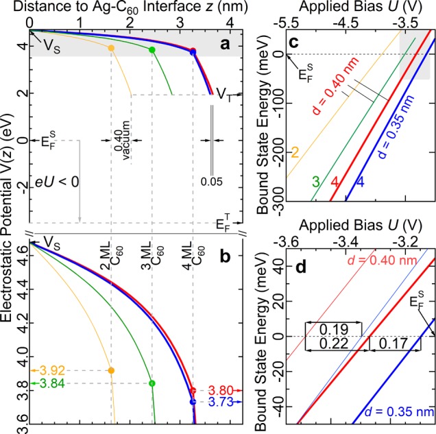
Calculated electrostatic potential and resultant split-off state potential energies. The orange, green, red, and blue curves are for a vacuum gap of d = 0.40, 0.40, 0.40, and 0.35 nm between the tip and C60 surface and a layer thickness of 2, 3, 4, and 4 ML C60, respectively. The sample and tip Fermi levels (EFS and EF), work functions (ΦS,ΦT) and vacuum levels (VS,VT) satisfy VS = EFS + ΦS and VT = EF + ΦT. (a) The potential directly beneath the tip for the bias U = −3.33 V. The Ag(111)-C60 interface is at z = 0. The solid circles denote the C60-vacuum interface. (b) Detail of the shaded region in (a). (c) The lowest LUMO split-off state energy as a function of U. (d) Detail of the shaded region in (c) with additionally, the second lowest singly degenerate LUMO split-off state shown with thin lines. The double-headed arrows indicate the voltage difference between where the curves cross zero energy, corresponding to EFS.
Figure 6c shows how the calculated lowest split-off state shifts with applied bias. The case of 4 ML C60 that is examined in detail in Figure 6d near EFS, in particular, shows how the two lowest split-off states depend on U and d. The lowest state moves below EF for U = −3.32 V which is comparable to U = −3.26 V as in experiments. U has to be lowered by an additional 0.22 V to move the second lowest peak through EFS, which is also comparable to experiment (see Figure 4d). Keeping the peak positions fixed as d is reduced from 0.4 to 0.35 nm requires a shift of 0.17 and 0.19 V, respectively. This gives the derivatives −3.5 (−3.8) V/nm compared with the experimental −1.95 (−2.16) V/nm for the lowest (second lowest) peak and qualitatively reproduces the expected electric field dependence seen in Figure 4d. The approximate factor of 2 discrepancy is considered reasonable given the approximations used in the calculations. Further refinement may require approximations that move beyond a spherical tip geometry and account for the orbital mixing between the Ag(111) substrate and C60. Because the theoretical model of the tip is sharper than a real tip, the calculations are expected to be biased in the direction of having a stronger electric-field dependence.36
We now discuss the Coulomb blockade that occurs when tunneling happens through a LUMO split-off state, and its relationship with the nonzero photon correlation dip shown in Figure 2c. Consider the DOS on the C60 molecule below the tip for U = −3.33 V (Figure 5c, red curve), and the change when a LUMO split-off state is occupied by one electron (Figure 5d, blue curve). Since the DOS are mostly localized on the C60 molecule below the tip, the associated Coulomb integrals are large. Thus, the electron occupancy just mentioned increases the electrostatic potential on the C60 below the tip by 1.02 eV and shifts the main structure in the LUMO DOS by 1.14 eV. The electrostatic potential on the neighbors of the molecule is increased by 0.34 eV, and the DOS is shifted correspondingly to higher energies. These changes prohibit the occupancy of any LUMO state by a second electron (Figure 5d, blue curve).
If tunneling only involved LUMO-derived states, this analysis would imply that a perfect Coulomb blockade should occur. However, the photon correlation dip, g(2)(t = 0), is clearly above 0, which is indicative of a finite probability that two photons can be emitted within picosecond intervals. To account for g(2)(t = 0) > 0, we suggest concomitant tunneling from the HOMO states, that is, in addition to the LUMO tunneling just discussed there is an additional HOMO tunneling component. The change between calculations in Figure 5c (red curve) and Figure 5d (blue curve) shows that the split-off states below the HOMO band edge shift up in energy when a LUMO state is occupied and becomes a resonant feature at −1.74 eV that is close to the top of the HOMO band. This has two consequences. The tunneling rate for a HOMO state is now substantially higher, since the electron has a higher energy when tunneling through the vacuum barrier. Thus, counterintuitively, the Coulomb blockade helps the tunneling of a HOMO electron. In addition, this electron may now have enough energy to emit a detectable photon when it decays to the Fermi level of the tip, EFS, at −3.33 V. If a photon detected at t = 0 were emitted by an electron tunneling from the HOMO resonance, a second electron could instantly tunnel from a LUMO split-off state and would reduce the g2(t) dip at t = 0. The sharp feature in Figure 3d measured on four layers at an applied bias of −3.26 V is then due to both tunneling through the LUMO split-off state and an increased tunneling through the resonance derived from HOMO split-off states. We envisage this latter contribution to be characterized explicitly by performing photon correlation experiments with spectral discrimination filters.
Our calculations predict that the Coulomb blockade can be overcome by the applied bias when it is lowered beyond U = −6.2 V. Only then can the tip potential move a LUMO split-off state, mainly localized in the innermost C60 layer, below EFS, even if an electron occupies a LUMO split-off state on the C60 below the tip. It would be interesting to characterize the behavior of the photon correlation in this situation.
Higher order tunneling mechanisms that occur should also reduce the nominal photon correlation dip. A HOMO electron, from a HOMO split-off state beneath the tip for instance, can tunnel even if the LUMO split-off states are empty. This creates a localized hole whose attractive potential causes the LUMO split-off states beneath the tip and the neighboring molecules to shift below EFS. The hole mitigates the Coulomb repulsion of housing two electrons within the 6 C60 states beneath the tip and the 36 C60 states of the neighboring molecules (counting spin and nominal T1u symmetry of the C60 LUMO) suddenly made energetically favorable for tunneling. The most important of these transient trion-like electronic configurations involves an electron on the same molecule as the hole and an additional electron on the same or neighboring molecule. The latter trion can only be formed by an electron hopping into the neighboring molecule first. The two electrons tunneling once the trion decays would then decrease the correlation dip.
Another possible reason for g(2)(t = 0) > 0 is that one tunneling electron can emit two photons,37 which is found to be important, in particular, for large tip–sample distances. We expect this effect to be small here, both because the tip–sample distance is rather small and because the bias is not much larger than twice the lower limit of the detector sensitivity. If two photons are emitted, then it is rather unlikely that both are detected, since energy conservation then requires that both have approximately the energy |U|/2.
To highlight some design guidelines for developing plasmonic antibunching emitters beyond C60, we have varied the parameters in our model calculations. First, we examine the energetics of making split-off states. We first double the LUMO and HOMO bandwidths, keeping their respective band edges closest to EFS, fixed relative to EF. To align a LUMO split-off state below EFS now requires roughly twice as large a bias as before. This proportional relationship favors the use of narrow bandwidth materials. Next, to favor antibunching, the tunneling contribution from the HOMO states should be lowered, for example, by reducing the large HOMO degeneracy (from 10 in the case of C60). Increasing the band gap of C60 from 2.3 eV38 by lowering the HOMO is also favorable. This change would lower the energy of the split-off state above the top of the HOMO that is present when a LUMO split-off state is occupied. This would then reduce the HOMO tunneling to the tip because the electron would now tunnel through a larger barrier and, thus, favor antibunching.
The effective on-site Coulomb interaction, Ueff, is also important39 and tends to be smaller for large molecules. Using molecules with a reduced Ueff would lower the energy of the HOMO split-off state which again favors antibunching. A material with a larger dielectric function would also reduce Ueff through screening effects. However, this change would require a larger bias voltage to make split-off states since the voltage drop over the molecular layers would be reduced. Electronegative molecules, such as C60, are favorable in this regard because a smaller bias is needed to pull a state below EFS.
Conclusions
We have shown that a local field can induce discrete states to appear in a molecular film on a metallic substrate in an STM setup, in analogy to those that appear in a quantum dot due to a confinement potential. This leads to a Coulomb blockade for tunneling charges evidenced by plasmonic photon antibunching. Here a C60-Ag(111) system was used, but we also discussed how other molecular characteristics could influence the emitter performance. We analyzed some possible reasons for the observed imperfect single photon emission, which revealed strategies to improve its performance. This approach reveals the possibility of using an external bias to regulate whether or not a Coulomb blockade occurs in a larger class of materials than previously thought, although large bandgap, narrowband materials are favored. In conventional quantum dots and single molecules, the maximum possible rate of single photon emission is limited by the exciton lifetime, which is often hard to influence and much longer than 1 ns. This long lifetime limits the rate at which single photon emission can be created from the emitter. Here, the explicit use of tunneling processes means that the rate has a sensitive exponential dependence on the tip–sample distance, and time scales shorter than 1 ns can be achieved if desired. The recovery time should also depend exponentially on the molecular layer thickness, which is given by the tunneling of electrons from the substrate into the split-off state at the surface of the C60 layer. Theoretically, it should increase exponentially with the distance over which the electron tunnels. While it is an effect awaiting experimental verification, it is anticipated that it can be controllably varied with conventional epitaxial techniques. This flexibility could broaden the class of materials that are useful for making single photon emitters. In summary, the significance of bypassing the use of excitons in single photon emission is that the rate of single photon production, or equivalently, the intensity, is no longer tied to the exciton lifetime. We anticipate future work to develop in these directions.
Methods
To make the samples, C60 is vapor deposited onto Ag(111) from a Knudsen cell for 1 h, with the sample temperature set between 213 and 253 K. This temperature range favors rough island growth, which then facilitates measuring the light emission as a function of layer thickness and STM parameters within a small rastered area. The resulting C60-Ag(111) topography and its characterization are shown in Figure 3a–d. The Ag(111) surface was prepared with standard cycles of Ar+ sputtering at 300 K, followed by annealing at 900 K. The STM tip is etched from a length of 99.995% pure Au wire of diameter 0.25 mm.
Acknowledgments
D. G. de Oteyza acknowledges support from the Alexander von Humboldt Foundation for his research stay at the MPI, hosted by K. Kern, as well as from the European Research Council under the European Union’s Horizon 2020 research and innovation programme (grant agreement no. 635919) and from the Spanish Ministry of Economy, Industry and Competitiveness (MINECO, grant no. MAT2016-78293-C6-1-R).
Supporting Information Available
The Supporting Information is available free of charge at https://pubs.acs.org/doi/10.1021/acsnano.9b09299.
The model of the C60 film, how its electronic structure is calculated, and the qualitative behavior of the HOMO and LUMO states at small bias. Supporting Figures include the calculated DOS for two and three layers of C60 on Ag(111). Control experiments showing constant g(2)(t) = 1. Tip–sample distance dependence of g(2)(t). Bias dependence of g(2)(t). Differential conductance (dI/dV) spectra for 4–7 ML C60. (PDF)
Author Present Address
◆ (A.R.) Université de Strasbourg, CNRS, IPCMS, UMR 7504, F-67000 Strasbourg, France.
Author Contributions
C. Leon, D. G. de Oteyza, A. Rosławska, P. Merino, A. Grewal, and K. Kuhnke performed the experimental work. C. Leon analyzed the experimental data. O. Gunnarsson performed the tight-binding calculations for the electronic structure of the Ag–C60-tip system. C. Leon and O. Gunnarsson wrote the manuscript with input from all authors. K. Kuhnke and K. Kern conceived and designed the research program.
The authors declare no competing financial interest.
Supplementary Material
References
- Slater J. C.The Electronic Structure of Solids. In Electrical Conductivity I/Elektrische Leitungsphänomene I. Series: Encyclopedia of Physics/Handbuch der Physik; Flügge S., Ed.; Springer: Berlin, 1956; pp 1–136. [Google Scholar]
- Yuan Z.; Kardynal B. E.; Stevenson R. M.; Shields A. J.; Lobo C. J.; Cooper K.; Beattie N. S.; Ritchie D. A.; Pepper M. Electrically Driven Single-Photon Source. Science 2002, 295, 102–105. 10.1126/science.1066790. [DOI] [PubMed] [Google Scholar]
- He Y.-M.; Clark G.; Schaibley J. R.; He Y.; Chen M.-C.; Wei Y.-J.; Ding X.; Zhang Q.; Yao W.; Xu X.; Lu C.-Y.; Pan J.-W. Single Quantum Emitters in Monolayer Semiconductors. Nat. Nanotechnol. 2015, 10, 497–502. 10.1038/nnano.2015.75. [DOI] [PubMed] [Google Scholar]
- Chakraborty C.; Kinnischtzke L.; Goodfellow K. M.; Beams R.; Vamivakas A. N. Voltage-Controlled Quantum Light from an Atomically Thin Semiconductor. Nat. Nanotechnol. 2015, 10, 507–511. 10.1038/nnano.2015.79. [DOI] [PubMed] [Google Scholar]
- Coe S.; Woo W.-K.; Bawendi M.; Bulović V. Electroluminescence from Single Monolayers of Nanocrystals in Molecular Organic Devices. Nature 2002, 420, 800–803. 10.1038/nature01217. [DOI] [PubMed] [Google Scholar]
- Kroupa D. M.; Vörös M.; Brawand N. P.; McNichols B. W.; Miller E. M.; Gu J.; Nozik A. J.; Sellinger A.; Galli G.; Beard M. C. Tuning Colloidal Quantum Dot Band Edge Positions through Solution-Phase Surface Chemistry Modification. Nat. Commun. 2017, 8, 15257. 10.1038/ncomms15257. [DOI] [PMC free article] [PubMed] [Google Scholar]
- Aharonovich I.; Englund D.; Toth M. Solid-State Single-Photon Emitters. Nat. Photonics 2016, 10, 631–641. 10.1038/nphoton.2016.186. [DOI] [Google Scholar]
- Tonndorf P.; Schmidt R.; Schneider R.; Kern J.; Buscema M.; Steele G. A.; Castellanos-Gomez A.; van der Zant H. S. J.; Michaelis de Vasconcellos S.; Bratschitsch R. Single-Photon Emission from Localized Excitons in an Atomically Thin Semiconductor. Optica 2015, 2, 347–352. 10.1364/OPTICA.2.000347. [DOI] [Google Scholar]
- Gunnarsson O.; Erwin S. C.; Koch E.; Martin R. M. Role of Alkali Atoms in A4C60. Phys. Rev. B: Condens. Matter Mater. Phys. 1998, 57, 2159–2162. 10.1103/PhysRevB.57.2159. [DOI] [Google Scholar]
- Blossey D. F. Wannier Exciton in an Electric Field. I. Optical Absorption by Bound and Continuum States. Phys. Rev. B 1970, 2, 3976–3990. 10.1103/PhysRevB.2.3976. [DOI] [Google Scholar]
- Dombrowski R.; Steinebach C.; Wittneven C.; Morgenstern M.; Wiesendanger R. Tip-Induced Band Bending by Scanning Tunneling Spectroscopy of the States of the Tip-Induced Quantum Dot on InAs(110). Phys. Rev. B: Condens. Matter Mater. Phys. 1999, 59, 8043–8048. 10.1103/PhysRevB.59.8043. [DOI] [Google Scholar]
- Imamoğlu A.; Yamamoto Y. Nonclassical Light Generation by Coulomb Blockade of Resonant Tunneling. Phys. Rev. B: Condens. Matter Mater. Phys. 1992, 46, 15982–15992. 10.1103/PhysRevB.46.15982. [DOI] [PubMed] [Google Scholar]
- Bauer G. E. W. Excitonic Correction to Resonant Tunneling. Surf. Sci. 1994, 305, 358–362. 10.1016/0039-6028(94)90916-4. [DOI] [Google Scholar]
- Senellart P.; Solomon G.; White A. High-Performance Semiconductor Quantum-Dot Single-Photon Sources. Nat. Nanotechnol. 2017, 12, 1026–1039. 10.1038/nnano.2017.218. [DOI] [PubMed] [Google Scholar]
- Wagner C.; Green M. F. B.; Leinen P.; Deilmann T.; Krüger P.; Rohlfing M.; Temirov R.; Tautz F. S. Scanning Quantum Dot Microscopy. Phys. Rev. Lett. 2015, 115, 026101. 10.1103/PhysRevLett.115.026101. [DOI] [PubMed] [Google Scholar]
- Zhu X.-Y.; Dutton G.; Quinn D. P.; Lindstrom C. D.; Schultz N. E.; Truhlar D. G. Molecular Quantum Well at the C60/Au(111) Interface. Phys. Rev. B: Condens. Matter Mater. Phys. 2006, 74, 241401. 10.1103/PhysRevB.74.241401. [DOI] [Google Scholar]
- Große C.; Merino P.; Rosławska A.; Gunnarsson O.; Kuhnke K.; Kern K. Submolecular Electroluminescence Mapping of Organic Semiconductors. ACS Nano 2017, 11, 1230–1237. 10.1021/acsnano.6b08471. [DOI] [PubMed] [Google Scholar]
- Hanbury Brown R.; Twiss R. Q. Interferometry of the Intensity Fluctuations in Light II. An Experimental Test of the Theory for Partially Coherent Light. Proc. R. Soc. London, Ser. A 1958, 243, 291–319. 10.1098/rspa.1958.0001. [DOI] [Google Scholar]
- Kuhnke K.; Kabakchiev A.; Stiepany W.; Zinser F.; Vogelgesang R.; Kern K. Versatile Optical Access to the Tunnel Gap in a Low-Temperature Scanning Tunneling Microscope. Rev. Sci. Instrum. 2010, 81, 113102. 10.1063/1.3480548. [DOI] [PubMed] [Google Scholar]
- David W. I. F.; Ibberson R. M.; Matthewman J. C.; Prassides K.; Dennis T. J. S.; Hare J. P.; Kroto H. W.; Taylor R.; Walton D. R. M. Crystal Structure and Bonding of Ordered C60. Nature 1991, 353, 147–149. 10.1038/353147a0. [DOI] [Google Scholar]
- Merino P.; Große C.; Rosławska A.; Kuhnke K.; Kern K. Exciton Dynamics of C60-Based Single-Photon Emitters Explored by Hanbury Brown-Twiss Scanning Tunnelling Microscopy. Nat. Commun. 2015, 6, 8461. 10.1038/ncomms9461. [DOI] [PMC free article] [PubMed] [Google Scholar]
- Merino P.; Rosławska A.; Große C.; Leon C. C.; Kuhnke K.; Kern K. Bimodal Exciton-Plasmon Light Sources Controlled by Local Charge Carrier Injection. Sci. Adv. 2018, 4, eaap8349 10.1126/sciadv.aap8349. [DOI] [PMC free article] [PubMed] [Google Scholar]
- Böckmann H.; Liu S.; Müller M.; Hammud A.; Wolf M.; Kumagai T. Near-Field Manipulation in a Scanning Tunneling Microscope Junction with Plasmonic Fabry-Pérot Tips. Nano Lett. 2019, 19, 3597–3602. 10.1021/acs.nanolett.9b00558. [DOI] [PMC free article] [PubMed] [Google Scholar]
- Zubizarreta Casalengua E.; López Carreño J. C.; del Valle E.; Laussy F. P. Structure of the Harmonic Oscillator in the Space of N-Particle Glauber Correlators. J. Math. Phys. 2017, 58, 062109. 10.1063/1.4987023. [DOI] [Google Scholar]
- Akimov A. V.; Mukherjee A.; Yu C. L.; Chang D. E.; Zibrov A. S.; Hemmer P. R.; Park H.; Lukin M. D. Generation of Single Optical Plasmons in Metallic Nanowires Coupled to Quantum Dots. Nature 2007, 450, 402–406. 10.1038/nature06230. [DOI] [PubMed] [Google Scholar]
- Zhang L.; Yu Y.-J.; Chen L.-G.; Luo Y.; Yang B.; Kong F.-F.; Chen G.; Zhang Y.; Zhang Q.; Luo Y.; Yang J.-L.; Dong Z.-C.; Hou J. G. Electrically Driven Single-Photon Emission from an Isolated Single Molecule. Nat. Commun. 2017, 8, 580. 10.1038/s41467-017-00681-7. [DOI] [PMC free article] [PubMed] [Google Scholar]
- Luo Y.; Chen G.; Zhang Y.; Zhang L.; Yu Y.; Kong F.; Tian X.; Zhang Y.; Shan C.; Luo Y.; Yang J.; Sandoghdar V.; Dong Z.; Hou J. G. Electrically Driven Single-Photon Superradiance from Molecular Chains in a Plasmonic Nanocavity. Phys. Rev. Lett. 2019, 122, 233901. 10.1103/PhysRevLett.122.233901. [DOI] [PubMed] [Google Scholar]
- Kolesov R.; Grotz B.; Balasubramanian G.; Stöhr R. J.; Nicolet A. A. L.; Hemmer P. R.; Jelezko F.; Wrachtrup J. Wave-Particle Duality of Single Surface Plasmon Polaritons. Nat. Phys. 2009, 5, 470–474. 10.1038/nphys1278. [DOI] [Google Scholar]
- Kalmeyer V.; Laughlin R. B. Differential Conductance in Three-Dimensional Resonant Tunneling. Phys. Rev. B: Condens. Matter Mater. Phys. 1987, 35, 9805–9808. 10.1103/PhysRevB.35.9805. [DOI] [PubMed] [Google Scholar]
- Buot F. A. Emitter Quantization and Double Hysteresis in Resonant-Tunneling Structures: A Nonlinear Model of Charge Oscillation and Current Instability. Phys. Rev. B 2000, 61, 5644–5665. [Google Scholar]
- Nazin G. V.; Wu S. W.; Ho W. Tunneling Rates in Electron Transport through Double-Barrier Molecular Junctions in a Scanning Tunneling Microscope. Proc. Natl. Acad. Sci. U. S. A. 2005, 102, 8832–8837. 10.1073/pnas.0501171102. [DOI] [PMC free article] [PubMed] [Google Scholar]
- Große C.; Kabakchiev A.; Lutz T.; Froidevaux R.; Schramm F.; Ruben M.; Etzkorn M.; Schlickum U.; Kuhnke K.; Kern K. Dynamic Control of Plasmon Generation by an Individual Quantum System. Nano Lett. 2014, 14, 5693–5697. 10.1021/nl502413k. [DOI] [PubMed] [Google Scholar]
- Veenstra S. C.; Heeres A.; Hadziioannou G.; Sawatzky G. A.; Jonkman H. T. On Interface Dipole Layers between C60 and Ag or Au. Appl. Phys. A: Mater. Sci. Process. 2002, 75, 661–666. 10.1007/s003390201311. [DOI] [Google Scholar]
- Hansson G. V.; Flodström S. A. Photoemission Study of the Bulk and Surface Electronic Structure of Single Crystals of Gold. Phys. Rev. B: Condens. Matter Mater. Phys. 1978, 18, 1572–1585. 10.1103/PhysRevB.18.1572. [DOI] [Google Scholar]
- Hebard A. F.; Haddon R. C.; Fleming R. M.; Kortan A. R. Deposition and Characterization of Fullerene Films. Appl. Phys. Lett. 1991, 59, 2109–2111. 10.1063/1.106095. [DOI] [Google Scholar]
- Urbieta M.; Barbry M.; Zhang Y.; Koval P.; Sanchez-Portal D.; Zabala N.; Aizpurua J. Atomistic-Scale Lighting Rod Effect in Plasmonic Picocavities: A Classical View to a Quantum Effect. ACS Nano 2018, 12, 585–595. 10.1021/acsnano.7b07401. [DOI] [PubMed] [Google Scholar]
- Leon C. C.; Rosławska A.; Grewal A.; Gunnarsson O.; Kuhnke K.; Kern K. Photon Superbunching from a Generic Tunnel Junction. Sci. Adv. 2019, 5, eaav4986 10.1126/sciadv.aav4986. [DOI] [PMC free article] [PubMed] [Google Scholar]
- Lof R. W.; van Veenendaal M. A.; Koopmans B.; Jonkman H. T.; Sawatzky G. A. Band Gap, Excitons, and Coulomb Interaction in Solid C60. Phys. Rev. Lett. 1992, 68, 3924–3927. 10.1103/PhysRevLett.68.3924. [DOI] [PubMed] [Google Scholar]
- Antropov V. P.; Gunnarsson O.; Liechtenstein A. I. Phonons, Electron-Phonon, and Electron-Plasmon Coupling in C60 Compounds. Phys. Rev. B: Condens. Matter Mater. Phys. 1993, 48, 7651–7664. 10.1103/PhysRevB.48.7651. [DOI] [PubMed] [Google Scholar]
Associated Data
This section collects any data citations, data availability statements, or supplementary materials included in this article.


