Abstract
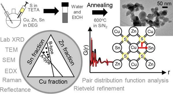
In the last decade, Cu2ZnSnS4 (CZTS) has been a promising earth-abundant, nontoxic candidate material for absorption layers within thin-film solar cells. One major issue preventing this type of solar cells from achieving competitive efficiency is impurity phases and structural defects in the bulk of the absorber; as a four-element compound, the formation of CZTS is highly sensitive to synthesis conditions. The impurity phases and defects differ by the fabrication method, and thus experimental characterization is vital for the successful development of CZTS photovoltaics. In this work, we characterize CZTS nanoparticles obtained by the hot-injection method and a standard N2/S annealing procedure. Phase-pure kesterite CZTS samples in the desired compositional range were characterized by standard means, i.e., Raman spectroscopy, X-ray diffraction, and energy-dispersive X-ray spectroscopy. However, using synchrotron X-ray diffraction with Rietveld refinement, we show that the as-synthesized nanoparticles consist of a mixture of the tetragonal and the fully disordered cubic sphalerite phase and transform into the tetragonal structure after heat treatment. Sn vacancies are seen in the annealed samples. X-ray total scattering with pair distribution function analysis furthermore suggests the presence of a nanostructured CZTS phase along with a bulk material. Finally, this study compares the benefits of applying synchrotron radiation instead of a standard laboratory X-ray diffraction when characterizing highly complex materials.
Introduction
Unlike traditional silicon solar cells, thin-film photovoltaics consists of materials with a high absorption coefficient, which allows for less material to be used in the construction of the cell.1 This could reduce the production costs and provide flexible films that can be integrated into buildings as well as be used in flexible electronics and power generation systems.2 Additionally, tandem architectures are considered as the next step in the continuous development of silicon solar cells and thin-film materials have suitable band gaps for this purpose.3−100 Thin-film Cu(In,Ga)(S,Se)2 (CIGS) and CdTe photovoltaics have already achieved power conversion efficiencies greater than 21% and are commercially available.5 Nevertheless, they contain toxic cadmium (Cd) and rare indium (In) and gallium (Ga), which prevents the large-scale utilization of these compounds. However, In and Ga in CIGS can be substituted with earth-abundant and nontoxic zinc (Zn) and tin (Sn), giving the kesterite Cu2ZnSnS4 (CZTS) structure.6 CZTS is a p-type semiconductor with an absorption coefficient higher than 104 cm–1 and an energy band gap of around 1.5 eV.7 Although the predicted power conversion efficiency according to the Shockley–Queisser limit is 31.6%,8,9 the current record efficiency is only 11%.10 This relatively low efficiency is attributed to a low open-circuit voltage (VOC), and the two major factors limiting the VOC value are the defective CZTS/CdS interface and structural defects in the bulk of the CZTS absorber.1 CZTS solar cells with high efficiencies consist of an off-stoichiometric Cu-poor and Zn-rich composition, and a careful control of synthesis conditions is required to circumvent the occurrence of secondary phases and intrinsic defects.11 Crystallographic defects related to Cu and Zn are the most likely to occur, and it has been assumed that CuZn antisite defects as well as VCu defects are the main acceptor defects in CZTS accounting for its p-type doping.11 The calculated stable chemical potential region for CZTS is narrow, which makes the synthesis of pure-phase CZTS challenging, as well as very sensitive to synthesis conditions. The narrow stable region is mainly restricted by the formation of ZnS and Cu2SnS3,12,13 and they form spontaneously when Zn is either in excess or deficient during the synthesis, respectively.12 Generally, the impact of secondary phases is still a subject of debate within the community.11,14 For example, although ZnS is an insulator that is supposed to be undesirable for charge transport, several groups have demonstrated high-efficiency devices, even including ZnS grains.5,15
CZTS can exist in various forms, and we present some relevant diamond-type crystal structures in Figure 1. The tetragonal kesterite and stannite phases are the most commonly observed structures.16 The structure desired for photovoltaic applications is kesterite. It is the most thermodynamically stable structure and thus most likely to form during synthesis.17 However, the formation energy of a stannite crystal is not much higher (2.8 meV/atom higher compared to kesterite).11 These structures are closely related as only the distribution of the Zn and Cu cations differs. The transition of kesterite CZTS into disordered kesterite is expected to occur around 260 °C,18 but a substantial amount of disorder has been detected at room temperature in all kesterite CZTS samples when characterized by neutron diffraction.14 At elevated temperatures of 866–1002 °C, tetragonal CZTS transforms into sphalerite,16,17,19 a fully disordered cubic structure. In some cases, the sphalerite phase has been found to coexist with the tetragonal phases even at room temperature.20−22 The structural similarity of the three phases and the almost identical X-ray scattering form factors of Cu+ and Zn2+ make the X-ray diffraction (XRD) patterns of the phases appear similar, as illustrated in Figure S1.
Figure 1.
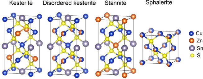
Selected diamond-type crystal structures of CZTS.
In this study, we investigate the as-synthesized and annealed nanoparticles of CZTS obtained by the hot-injection method, previously described by Mirbagheri et al.23 Unlike most nanoparticle approaches, the as-synthesized particles are organic ligand-free, and absorbers without the infamous carbon-rich “fine grain layer” at the back interface have been demonstrated.24 The synthesis approach is fast, upscalable, and ensures low material losses. Contrary to the precursor salt approach, the nanoparticle approach allows for numerous coating techniques as ink properties are easily tuned.25 Therefore, this method has the potential to sustain the terawatt-scale fabrication of thin-film photovoltaics. By a comprehensive study using synchrotron X-ray diffraction with Rietveld refinement, X-ray total scattering with pair distribution function (PDF) analysis, and transmission electron microscopy (TEM), we gain a new insight into the material quality compared to characterization with the more standard techniques such as laboratory XRD analysis and scanning electron microscopy/energy-dispersive X-ray spectroscopy (SEM/EDX) characterization.
Results and Discussion
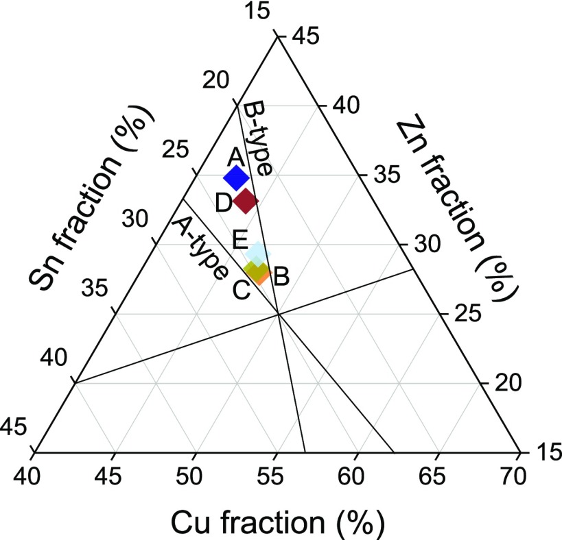
Five different CZTS nanoparticle samples were synthesized via the hot-injection route, previously described in our earlier work.23 We aimed at off-stoichiometric Cu-poor and Zn-rich compositions without any secondary phases or unwanted intrinsic defects, as these are supposed to provide the highest efficiencies.26 Results from EDX measurements of the five different samples are shown in Table 1 and Figure 2. All samples were Cu-poor and Zn-rich, and compositions appear to change after the thermal treatment.
Table 1. Reaction Conditions and Elemental Compositions of the Investigated Samples.
| SnCl4 (mmol) | synthesis temp (°C) | composition before annealing | composition after annealing | |
|---|---|---|---|---|
| A | 0.23 | 228 | Cu1.7Zn1.0SnS3.1 | Cu1.9Zn1.5SnS4.1 |
| B | 0.21 | 228 | Cu1.9Zn1.1SnS3.6 | Cu1.9Zn1.1SnS3.9 |
| C | 0.19 | 231 | Cu2.3Zn1.3SnS4.3 | Cu1.9Zn1.1SnS3.8 |
| D | 0.19 | 221 | Cu2.1Zn1.4SnS4.0 | Cu1.9Zn1.5SnS4.3 |
| E | 0.19 | 231 | Cu2.2Zn1.2SnS4.0 | Cu1.9Zn1.2SnS3.8 |
Figure 2.
Compositional map of samples after annealing. The desired compositional range lies between the A- and B-type lines.
All annealed samples have band gaps of about 1.44 eV, as measured by diffuse reflectance using the Kubelka–Munk model (Figure 3).27 The theoretical band gap for CZTS is about 1.47–1.65 eV for kesterite and 1.27–1.40 eV for stannite.7 The optical band gap of CZTS estimated by diffuse reflectance is reportedly 0.05 eV lower than the value obtained by the transmittance technique.28 Taking this into account, a value of 1.44 eV is consistent with kesterite CZTS according to literature values.
Figure 3.
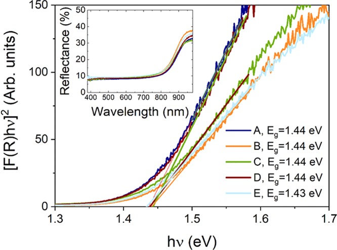
Band gap determination for the annealed CZTS powders using the Kubelka–Munk formalism. The inset shows optical reflectance as a function of wavelength.
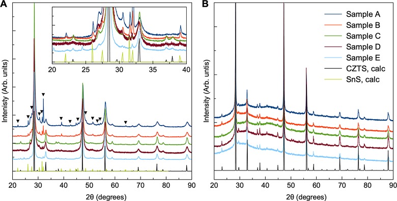
The XRD patterns obtained by a standard laboratory diffractometer of the samples before and after annealing are shown in Figure 4A,B, respectively. Each sample appears to contain the pure kesterite CZTS structure both before and after thermal treatment, as seen when comparing with the calculated CZTS pattern. However, it should be noted that the stannite and kesterite structures are almost indistinguishable from XRD alone, as illustrated in Figure S1. For the as-synthesized samples, the considerable peak broadening indicates that the particles are nanosized. After annealing, the XRD peaks have sharpened, suggesting particle growth during the heat treatment.
Figure 4.
XRD patterns of as-synthesized (A) and annealed (B) powders obtained by a standard diffractometer. The reference kesterite CZTS pattern is shown in black, the SnS reference pattern in green, and the SnS peaks are marked by (▼). SnS is present in each as-synthesized powder except from C, along with unidentified phases as shown in the inset in (A). The thermal treatment appears to purify the CZTS phase.
Before thermal treatment, the XRD patterns reveal the presence of several impurity phases including SnS in samples A, B, D, and E, while after thermal treatment, the laboratory XRD patterns appear to show phase-pure kesterite. However, when considering synchrotron XRD patterns (Figure 5), several secondary phases are detected in the annealed samples. Rietveld refinements of the data will be discussed further below. Samples A, B, and D contain a small amount of SnS, and Cu4SnS4 is furthermore seen in sample A. Peaks from unidentified compounds are marked by “+” (in particular in samples C and D). Moreover, a minor peak for sample D at 2θ = 2.76° suggests yet another phase. Sample E appears phase pure, as the additional scattering intensity around the (112) Bragg peak at 2θ = 3.87° in the XRD pattern of powder E is likely to originate from planar defects (marked by “x”), as previously described by Mainz et al.29 The fact that secondary phases are clearly visible only in the synchrotron scattering data stresses that very high-quality X-ray diffraction data (with high angular resolution and high signal-to-noise ratio) are needed to fully characterize the samples.
Figure 5.
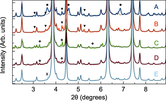
Synchrotron XRD patterns of annealed CZTS powders. The black solid lines correspond to the fitted CZTS patterns. The data reveal several secondary phases, including SnS (▼), Cu4SnS4 (●), planar defects (x), and unidentified compounds (+).
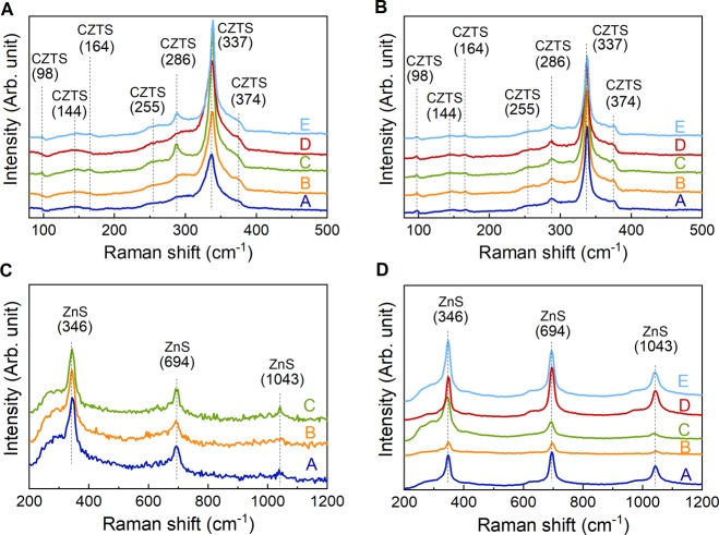
To further reveal or confirm the existence of secondary phases, Raman spectroscopy was carried out, and the Raman spectra of as-synthesized and annealed powders are shown in Figure 6 with both 532 and 325 nm lasers. The Raman peaks become sharper upon annealing, which can be associated with a higher degree of crystallinity as also seen in the XRD data. The data from the green laser (Figure 6A,B) confirm the kesterite phase in all as-synthesized and annealed samples with its main peak located at 337 cm–1 (mode A).30,31 In addition, some samples display Raman peaks at 286 and 374 cm–1 (mode E/B-TO LO) as well as a weak hump at 144 cm–1 (mode E-TO LO), which are characteristic of the kesterite CZTS structure.30,31 The Raman data show no clear signs of any secondary Cu–Sn–S phases (located at 318, 303/356, and 290/352 cm–1 for orthorhombic Cu3SnS4, cubic Cu2SnS3, and monoclinic Cu2SnS3, respectively),32,33 which suggests either that none exist or it may be related to the poor detection sensitivity or the relatively small volume probed by confocal Raman spectroscopy. For certain sites on the samples, a SnS phase was detected in the as-synthesized powders by displaying peaks located at 95, 164, 192, and 218 cm–1, as shown in Figure 7.34 During heat treatment, SnS either evaporated or underwent another type of phase transformation such that no traces remain on the surface according to Raman measurements. The SnS phase could also be detected by EDX (data not shown) as flakelike features in all as-synthesized samples except sample C, as illustrated in the SEM images in Figure 7. The lack of detected secondary phases in the annealed samples from Raman spectroscopy contradicts the XRD findings and emphasizes the high sensitivity of the synchrotron XRD data. The UV Raman spectra (Figure 6C,D) furthermore reveal the presence of ZnS in all samples investigated both before and after thermal treatment. In the discussion above, ZnS was not observed from X-ray diffraction due to the overlap with peaks from the CZTS phase.
Figure 6.
Raman spectra of (A) as-synthesized and (B) annealed powders obtained with λ = 532 nm laser, and of the (C) as-synthesized and (D) annealed powders obtained with λ = 325 nm laser. Both CZTS and ZnS are present in all samples, and thermal treatment enhances the intensity of the Raman spectra.
Figure 7.
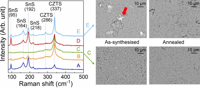
Raman spectra of as-synthesized powders obtained with a 532 nm laser, as well as SEM images of as-synthesized and annealed samples C and E. The Raman spectra reveal the presence of SnS in all as-synthesized samples except sample C. SnS can be recognized in the SEM image as flakes, marked with a red arrow in the as-synthesized sample E.
TEM images were collected for the annealed samples (Figures 8 and S2). The annealed CZTS particles have a broad size distribution, with diameters ranging from three to hundreds of nanometers. Comparing these data with the size distribution of an as-synthesized powder from a similar synthesis recipe (23 ± 11 nm),23 we conclude that the thermal treatment results in particle growth, consistent with the XRD data.
Figure 8.
TEM images of the annealed sample E. The planar defects (green arrows) and organic surface layers at the edges (gray arrows) are present in all annealed samples (Figure S2).
The annealed powders exhibit characteristic striped patterns indicated by the black arrows in Figure 8. This could suggest the presence of twin planar defects, as previously observed by Kattan et al.35 and Ahmad et al.36 According to their findings, the border between twin planes stems from stacking faults where the local packing changes from a cubic to hexagonal structure.35,36 Notably, the CZTS nanoparticles investigated by Kattan et al.35 and Ahmad et al.36 were obtained by the hot-injection method and were found to have shapes and sizes similar to those of the samples considered in this work. In addition, the uneven edges of the CZTS particles suggest an amorphous—perhaps organic—surface layer surrounding the crystals (see the gray arrows in Figure 8).
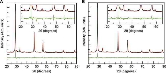
Next, we apply Rietveld refinement to extract more information about the crystal structures from the collected XRD data. The laboratory XRD pattern of the as-synthesized powders can be reasonably well described by the CZTS phase, as shown for sample C (containing the least secondary phases) in Figure 9A. The refinement results and fits for samples A, B, D, and E can be found in the Supporting Information Figures S3–S8. However, while the main Bragg peak positions are described by the model, the kesterite structure fails to fully model their intensities. When attempting to refine the atomic displacement parameters (ADPs), unphysically large values were obtained for the Sn site, while refinement of the ADPs for other cation sites resulted in negative values, indicating structural disorder. On further examining the difference curve (Figure 9A), it is clear that the modeled intensities of peaks originating from cation ordering (in space group I4̅) are too large compared to the data, while the opposite is seen for the main, most intense peaks, which are also present in the diffraction pattern from the sphalerite structure (space group F4̅3m) (Figure S1). This indicates that the as-synthesized samples do not take a fully cation-ordered structure. On fitting the data with a two-phase model, using both the ordered kesterite and disordered sphalerite structures (representing either ZnS and disordered CZTS, respectively), a better description of the peak intensities is obtained, as illustrated in Figure 9B for sample C. This effect is seen for all five samples. Note that the model is kept simple to account for the limited data quality, and all ADP values were kept fixed at Biso = 1.0 Å2. The Rietveld results of the as-synthesized samples furthermore give average, volume-weighted crystallite sizes for each of the samples, calculated using the Scherrer formula taking into account instrumental broadening. These range from 9 to 22 nm (Table 2).
Figure 9.
Rietveld refinement of the as-synthesized sample C. (A) Refinement with the CZTS kesterite phase. (B) Two-phase refinement with the kesterite and sphalerite phases. In all fits, the data are shown in black, the model in red, and the difference between the two in green. The insets show a magnification of the difference curve.
Table 2. Main Results from Rietveld Refinements of the As-Synthesized Samplesa.
| a (Å) | c (Å) | Scherrer crystallite size (nm) | |
|---|---|---|---|
| A | 5.433(3) | 10.79(1) | 9.1 |
| B | 5.434(2) | 10.81(1) | 12.8 |
| C | 5.433(1) | 10.82(1) | 21.0 |
| D | 5.436(1) | 10.79(1) | 11.4 |
| E | 5.433(1) | 10.82(1) | 21.9 |
More details are given in the Supporting Information.
Results from Rietveld refinement of the synchrotron XRD data obtained from the annealed samples are summarized in Table 3 and Figures S9–S13. The fit obtained for sample E is shown in Figure 10. For the annealed samples, the average crystallite size is too large to give significant peak broadening, and average crystallite sizes are therefore not extracted from the data. As illustrated in Figure 5, secondary phases are seen in the annealed samples apart from sample E, where all significant peaks can be indexed to the CZTS structure.
Table 3. Main Results from Rietveld Refinements of the Annealed Samplesa.
| RBragg (%) | a (Å) | c (Å) | Sn 2b occupancy | |
|---|---|---|---|---|
| A | 6.39 | 5.433(1) | 10.838(5) | 0.95(2) |
| B | 3.80 | 5.433(1) | 10.834(3) | 0.94(2) |
| C | 4.63 | 5.433(2) | 10.837(7) | 0.96(1) |
| D | 2.61 | 5.433(1) | 10.840(3) | 0.94(1) |
| E | 2.70 | 5.433(1) | 10.837(3) | 0.92(1) |
More details are given in the Supporting Information.
Figure 10.
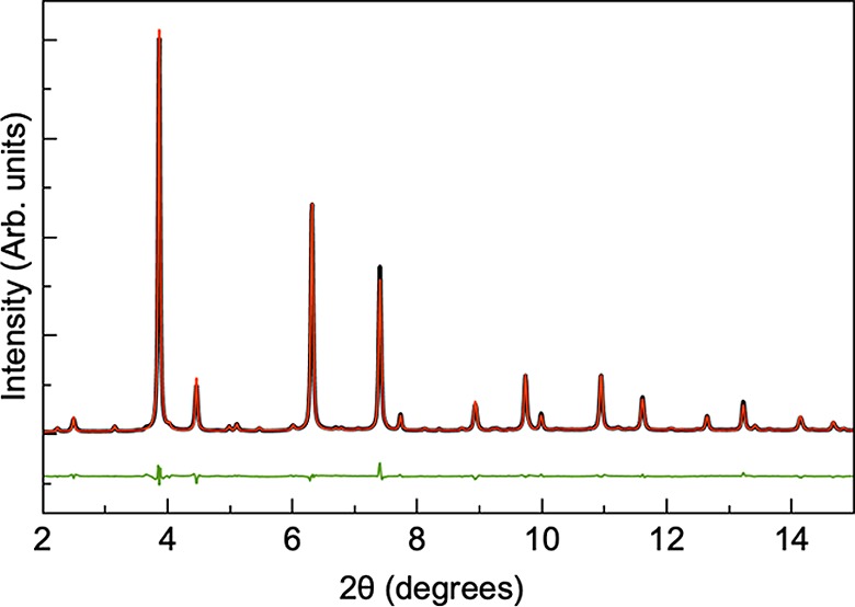
Rietveld refinement of the annealed sample E. The data are shown in black, the calculated model in red, and the difference between the two in green.
Generally, for the annealed samples, the bulk CZTS model gives a very good description of the data, and the difference in fit agreement values (RBragg) between the five samples (Table 3) reflects mainly the presence of secondary phases that are not described by the model. As discussed above, it is not possible to characterize the presence of Cu/Zn disorder in the samples from X-ray diffraction due to the almost identical X-ray scattering powers of Cu+ and Zn2+. However, when refining the site occupancies of the metal sites in the structure, the refinement was improved and consistently showed slightly lower electron densities on the Cu 2c and Sn 2b sites in the structure, as illustrated in Table 3. Vacancies on the Sn sites have previously been reported in the literature, and such vacancies have energy levels deep within the band gap of CZTS.12 While crystallographic defects involving the Sn site have higher formation energies than many other defects, which makes them unlikely to form, specific environmental conditions during synthesis could result in the reduction of its formation energy,1 and even low concentrations of these defects would be detrimental to the device. Ongoing work in the field involves minimizing the presence of these Sn-related defects by incorporating foreign group IV elements such as Ge into the structure37 or by tuning the Sn composition. Larramona et al. showed that by fine-tuning the Sn concentration in Cu2ZnSn(S1–xSex)4 (CZTSSe) absorbers, the formation of a deep defect at around 600 meV could be avoided and the device performance could be improved.38
To further characterize the CZTS structure, we apply PDF analysis. The PDF is obtained as a Fourier transform of, e.g., X-ray total scattering data so that scattering data analysis can be done in r-space: The PDF represents a histogram of interatomic distances in the sample, and each peak can be assigned to atomic pairs in the structure.39 As the total scattering signal (rather than only Bragg peaks, as done in Q-space Rietveld refinement) is included in the analysis, it is possible to analyze, e.g., nanostructures where long-range order is lacking.40
Figure 11 shows the PDF calculated from X-ray total scattering data of the annealed sample E. The bulk kesterite model gives an excellent match when fitted to the long-range order (7–50 Å), as expected from the Q-space Rietveld refinements discussed above. However, when extending the model to the local range, the difference curve shows distinct features at 3.8, 6.7, and 10.3 Å, where the intensities of the PDF peaks are not fully described. These peaks correspond to metal–metal interatomic distances in the kesterite structure, and the misfit indicates the existence of an additional nanoscale phase with only local-range order. When considering the TEM images, some small (few nanometers) nanoparticles were seen along with much larger ones, and thus an extra nanostructured phase in addition to the kesterite structure was introduced in the model, which lowered the RW value over the full range of 7.7–6.0%. As seen in the refinements in Figure S18, the results showed that the nanoparticle phase makes up approximately 19% of the sample. Similar results were obtained for samples A–D, as illustrated in Figures S14–S17, showing that small nanoparticles exist in all samples. Note that we have used the same CZTS model to describe the nanostructured phase and the bulk phase, but future neutron scattering experiments could reveal whether the cation disorder often discussed in CZTS is size-dependent.
Figure 11.
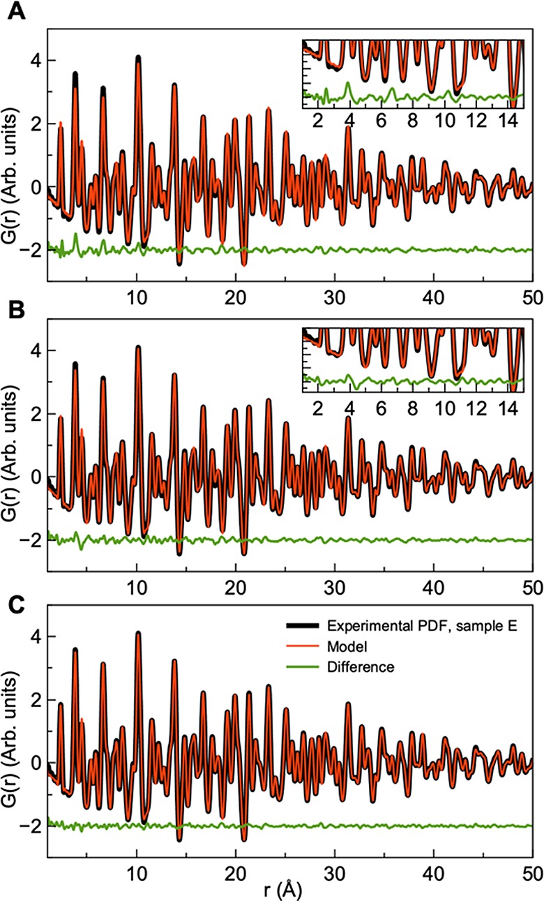
PDF fits of the PDF obtained for annealed sample E. (A) Fit with the CZTS kesterite phase. The model was refined in the r-range 6–50 Å and then extended to the local range. (B) Fit with two CZTS kesterite phases: One describing large particles and the other describing small (3 nm) nanoparticles. (C) Fit with two CZTS phases and S vacancies. Results are given in the Supporting Information.
Considering the fit including the nanostructured phase shown in Figure 11B, it is clear that a misfit still exists in the local region. The intuitive nature of the PDF allows us to investigate this for further structural insight. The peak seen at approximately 3.82 Å corresponds to the first Cu/Zn–Cu/Zn and Cu/Zn–Sn distance in the structure. The peak next to it, at approximately 4.5 Å corresponds to the second metal–S distance. In the model, this metal–sulfur peak has a very high intensity compared to the metal–metal peak at 3.82 Å, which could indicate the presence of S vacancies in the structure. As illustrated in Figure 11C, the fit quality increases (RW = 4.6%) by allowing S vacancies in the model. The refinement results show up to 15% S vacancies, although this number is associated with large uncertainties, which are difficult to estimate in PDF analysis. Surprisingly, we did not identify S vacancies in the Q-space Rietveld refinements, but they clearly manifest themselves in the PDF after the addition of a nanostructured phase to the refinements. However, to fully characterize the defect chemistry in the samples, neutron scattering data are needed.
To conclude whether the detected defects and impurities have an effect on device performance, solar cells should be fabricated. The amount of secondary phases present is lower than the detection limit of a standard laboratory XRD, and the techniques used here give us a window to observe structural effects, e.g., microinhomogeneities which otherwise are not detectable, but may influence the performance of devices. To improve the purity of the annealed compound further, a better control and understanding of the annealing conditions are required as well. Additionally, the inclusion of a foreign group IV element such as Ge into the structure would minimize the presence of Sn-related defects.37
To utilize the synchrotron scattering characterization approach presented here, a relatively large amount of powder is required when applying routine measurement techniques, which limits which thin-film deposition approaches are appropriate for standard technique. However, the characterization methods can provide a new insight into certain solution techniques and other approaches for mass production.
Conclusions
In this work, we have investigated kesterite samples by standard laboratory X-ray diffraction, synchrotron X-ray diffraction, and X-ray total scattering along with Raman scattering, scanning electron microscopy, and transmission electron microscopy. The samples were prepared by the inexpensive and environmentally friendly hot-injection method. We note that the hot-injection synthesis does not result in a product as homogeneous as expected. However, this was only clear after taking advantage of the much better detection sensitivity obtained with synchrotron X-ray diffraction compared to laboratory X-ray diffraction. Second, we found that the as-synthesized nanoparticles consisted of a mixture of the tetragonal and cubic sphalerite phases and all samples transform into the tetragonal structure after heat treatment. The use of PDF analysis showed that small CZTS nanoparticles of size 3–5 nm coexisted with much larger crystals in the annealed samples. Furthermore, we have detected problematically lowered electron densities on the Sn 2b site, which suggests the existence of so-called “killer defects” and underlines the importance of incorporating foreign cations into the material to minimize such defects. The PDF analysis furthermore indicated S vacancies, and other issues involve secondary phases, including ZnS, SnS, and Cu4SnS4, and an amorphous surface layer surrounding the nanoparticles, as well as planar defects within the particles.
Experimental Section
Sample Preparation
The CZTS nanoparticles were synthesized via the hot-injection route described in our earlier work.23 We aimed at off-stoichiometric Cu-poor and Zn-rich compositions without any secondary phases. To achieve the desired composition in the final product, the temperature and the amount of tin(IV) chloride pentahydrate (SnCl4·5H2O, 98%, Sigma-Aldrich) in the reaction medium were varied accordingly (see Table 1). The nanoparticles were either dispersed in ethanol or coated as thin films onto soda lime substrates for further characterization or annealed as a powder on soda lime glass. The annealing was carried out for 30 min at a nominal temperature of 600 °C in a quartz tube vacuum oven at a nitrogen pressure of 100 mbar; the samples were placed inside a graphite box with 100 mg of S powder to prevent the loss of S.
Diffuse Reflectance
Optical band gaps were determined by converting the diffuse reflectance to the equivalent absorption coefficient, F(R), using the Kubelka–Munk model, as described in Davidsdottir et al.27 The optical measurements were carried out with an integrating sphere setup of reflectance geometry 8°/d. The collimated beam from a deuterium tungsten-halogen light source (type DH-2000-BAL from Ocean Optics) was coupled to the integrating sphere through an optical fiber of 600 μm core diameter (F0-2-SR from Ocean Optics). The band gap (Eg) was determined from the equivalent Tauc plots ([F(R) × hν]2 versus photon energy (hν)) as the intersection between the x-axis and the linear extrapolation of the graph.
Raman Spectroscopy
Raman measurements were performed using a Renishaw spectrometer (inVia Raman Microscope) equipped with a charge-coupled device (CCD) detector. A diode-pumped solid-state laser with a wavelength of 532 nm was used for excitation. The measurements were performed in backscattering configuration using a laser power of 0.1 mW and a spot size of 2 × 2 μm2. In addition, a near-ultraviolet He–Cd laser with a wavelength of 325 nm and a laser power of 20 mW was used. Each spectrum represents an integration over 10 s and an average over 15 measurements in five different regions of a sample.
Electron Microscopy
Samples for TEM measurements were prepared on a Cu grid with a lacey carbon support film. We used an FEI Tecnai T20 microscope with a LaB6 filament, running at a 200 kV accelerating voltage. The images were acquired on a Gatan Ultrascan CCD camera.
The chemical composition was estimated by EDX performed with an accelerating voltage of 15 kV with a Bruker Quantax 70 system integrated into a Hitachi TM3000 SEM.
X-ray Diffraction
Standard laboratory XRD measurements were carried out in the 2θ range of 5–90° using a Bruker D8 Advance diffractometer with Cu Kα radiation. For further structural characterization, synchrotron XRD and X-ray total scattering data were obtained on the annealed powders. The synchrotron data were obtained at beamline 11-ID-B at the Advanced Photon Source at Argonne National Laboratory (Chicago). The X-ray wavelength was λ = 0.2118 Å.
Rietveld Refinement
The standard, laboratory XRD data from the as-synthesized samples were analyzed with Rietveld refinement, using the bulk kesterite model in space group I4̅. Refinements were done in FullProf Suite.41 The peak profiles were described using the Thompson–Cox–Hastings pseudo-Voigt model, and instrumental broadening was taken into account through the analysis of a corundum standard sample. The background was refined using a 12-term Chebyshev polynomial. Due to the limited data quality, the number of parameters in the refinement was kept low: Apart from the background parameters, the scale factor was refined along with the unit cell parameters (a and c) and the Y parameter describing peak broadening from the small crystallite size. A zero-point error was also refined. For sample C, an additional refinement including a sphalerite phase (based on ZnS) was performed, where the sphalerite scale factor, unit cell parameter, and size broadening parameter were also included. The isotropic atomic displacement parameters (ADPs) for all atomic sites were kept fixed at Biso = 1.0 Å2. The refined sample peak broadening parameter Y was used to calculate the crystallite size through the Scherrer formula.
The synchrotron XRD data for the annealed samples were also modeled with the kesterite I4̅ structure, using the Thompson–Cox–Hastings pseudo-Voigt model for peak shape and treating the background with Chebyshev polynomials. The scale factor was refined along with the unit cell parameters (a and c); the peak profile parameters Y, U, and V; a zero-point error; the fractional coordinates for S; isotropic ADPs for all sites; and the occupancy for the Cu 2a site and the Sn 2d site.
Pair Distribution Function Analysis
The X-ray total scattering data were Fourier transformed in xPDFsuite using PDFgetX342 and modeled using PDFgui.43 Two different models were used: First, the data were modeled with the kesterite model taking the refined structure from the Q-space Rietveld refinements as a starting point. The scale factor, unit cell parameters, ADPs for all sites, as well as the atomic coordinates for the S site were refined. A parameter describing correlated atomic motion (delta2) was furthermore used, as well as a parameter (Qdamp) describing instrumental damping of the PDF. In the second model, an additional kesterite CZTS phase was introduced in the refinements, describing small nanoparticles. A scale factor and particle size (assuming spherical particles) for the second phase were refined. The structural parameters of the second phase were kept the same as the bulk CZTS phase, except for the unit cell parameters.
Acknowledgments
Work in the Schou group at DTU Fotonik was supported by a grant from the Innovation Fund Denmark (the ALTCELL project). The authors acknowledge the assistance of Jens Kling from DTU CEN for the preparation of TEM images. Work in the Jensen group was supported by the Villum Foundation through a Villum Young Investigator grant. The authors furthermore thank DANSCATT (supported by the Danish Agency for Science and Higher Education) for support. Use of the Advanced Photon Source at Argonne National Laboratory was supported by the U.S. Department of Energy, Office of Science, Office of Basic Energy Sciences, under Contract no. DE-AC02-06CH11357.
Supporting Information Available
The Supporting Information is available free of charge at https://pubs.acs.org/doi/10.1021/acsomega.0c00657.
Calculated diffraction patterns for the stannite, kesterite and sphalerite structures; TEM images of all particles at different magnification; Rietveld refinement of laboratory XRD data obtained for as-synthesized samples; Rietveld refinement of synchrotron XRD data obtained for annealed samples; fit of the PDF obtained for annealed samples, using two CZTS phases of different domain sizes (PDF)
Author Present Address
∥ Department of Physics, University of Cambridge, JJ Thomson Ave, Cambridge CB3 0HE, United Kingdom.
Author Contributions
§ S.E. and J.Sy. contributed equally to this work.
The authors declare no competing financial interest.
Supplementary Material
References
- Wallace S. K.; Mitzi D. B.; Walsh A. The Steady Rise of Kesterite Solar Cells. ACS Energy Lett. 2017, 2, 776–779. 10.1021/acsenergylett.7b00131. [DOI] [Google Scholar]
- Polman A.; Knight M.; Garnett E. C.; Ehrler B.; Sinke W. C. Photovoltaic materials: Present efficiencies and future challenges. Science 2016, 352, aad4424 10.1126/science.aad4424. [DOI] [PubMed] [Google Scholar]
- Green M. A. Commercial progress and challenges for photovoltaics. Nat. Energy 2016, 1, 15015 10.1038/nenergy.2015.15. [DOI] [Google Scholar]
- Green M. A. Photovoltaic technology and visions for the future. Prog. Energy 2019, 1, 013001 10.1088/2516-1083/ab0fa8. [DOI] [Google Scholar]
- Martinho F.; Hajijafarassar A.; Lopez-Marino S.; Espindola-Rodriguez M.; Engberg S.; Gansukh M.; Stulen F.; Grini S.ør.; Canulescu S.; Stamate E.; Crovetto A.; Vines L.; Schou J.; Hansen O. Nitride-Based Interfacial Layers for Monolithic Tandem Integration of New Solar Energy Materials on Si: The Case of CZTS. ACS Appl. Energy Mater. 2020, 10.1021/acsaem.0c00280. [DOI] [Google Scholar]
- Green M. A.; Hishikawa Y.; Dunlop E. D.; Levi D. H.; Hohl-Ebinger J.; Yoshita M.; Ho-Baillie A. W. Y. Solar cell efficiency tables (Version 53). Prog. Photovolt: Res. Appl. 2019, 27, 3–12. 10.1002/pip.3102. [DOI] [Google Scholar]
- Katagiri H.; Sasaguchi N.; Hando S.; Hoshino S.; Ohashi J.; Yokota T. Preparation and evaluation of Cu2ZnSnS4 thin films by sulfurization of E-B evaporated precursors. Sol. Energy Mater. Sol. Cells 1997, 49, 407–414. 10.1016/S0927-0248(97)00119-0. [DOI] [Google Scholar]
- Persson C.; Chen R.; Zhao H.; Kumar M.; Huang D.. Electronic Structure and Optical Properties from First-Principles Modeling. In Copper Zinc Tin Sulfide-Based Thin-Film Solar Cells, 1st ed.; Ito K., Ed.; John Wiley & Sons: West Sussex, U.K., 2015; pp 75–102. [Google Scholar]
- Shockley W.; Queisser H. J. Detailed Balance Limit of Efficiency of p-n Junction Solar Cells. J. Appl. Phys. 1961, 32, 510 10.1063/1.1736034. [DOI] [Google Scholar]
- Rühle S. Tabulated values of the Shockley–Queisser limit for single junction solar cells. Sol. Energy 2016, 130, 139–147. 10.1016/j.solener.2016.02.015. [DOI] [Google Scholar]
- Yan C.; Huang J.; Sun K.; Johnston S.; Zhang Y.; Sun H.; Pu A.; He M.; Liu F.; Eder K.; Yang L.; Cairney J. M.; Ekins-Daukes N. J.; Hameiri Z.; Stride J. A.; Chen S.; Green M. A.; Hao X. Cu2ZnSnS4 solar cells with over 10% power conversion efficiency enabled by heterojunction heat treatment. Nat. Energy 2018, 3, 764–772. 10.1038/s41560-018-0206-0. [DOI] [Google Scholar]
- Schorr S.Crystalloaphic Aspects of Cu2ZnSnS4 (CZTS). In Copper Zinc Tin Sulfide-Based Thin-Film Solar Cells, 1st ed.; Ito K., Ed.; John Wiley & Sons: West Sussex, U.K., 2015; pp 55–74. [Google Scholar]
- Chen S.; Walsh A.; Gong X.-G.; Wei S.-H. Classification of Lattice Defects in the Kesterite Cu2ZnSnS4 and Cu2ZnSnSe4 Earth-Abundant Solar Cell Absorbers. Adv. Mater. 2013, 25, 1522–1539. 10.1002/adma.201203146. [DOI] [PubMed] [Google Scholar]
- Huang D.; Persson C. Band gap change induced by defect complexes in Cu2ZnSnS4. Thin Solid Films 2013, 535, 265–269. 10.1016/j.tsf.2012.10.030. [DOI] [Google Scholar]
- Ritscher A.; Hoelzel M.; Lerch M. The order-disorder transition in Cu2ZnSnS4 – A neutron scattering investigation. J. Solid State Chem. 2016, 238, 68–73. 10.1016/j.jssc.2016.03.013. [DOI] [Google Scholar]
- Larramona G.; Bourdais S.; Jacob A.; Choné C.; Muto T.; Cuccaro Y.; Delatouche B.; Moisan C.; Péré D.; Dennler G. Efficient Cu2ZnSnS4 solar cells spray coated from a hydro-alcoholic colloid synthesized by instantaneous reaction. RSC Adv. 2014, 4, 14655–14662. 10.1039/C4RA01707B. [DOI] [Google Scholar]
- Schorr S. The crystal structure of kesterite type compounds: A neutron and X-ray diffraction study. Sol. Energy Mater. Sol. Cells 2011, 95, 1482–1488. 10.1016/j.solmat.2011.01.002. [DOI] [Google Scholar]
- Bosson C. J.; Birch M. T.; Halliday D. P.; Knight K. S.; Gibbs A. S.; Hatton P. D. Cation disorder and phase transitions in the structurally complex solar cell material Cu2ZnSnS4. J. Mater. Chem. A 2017, 5, 16672–16680. 10.1039/C7TA03603E. [DOI] [Google Scholar]
- Scragg J. J.; Choubrac L.; Lafond A.; Ericson T.; Platzer-Björkman C. A low-temperature order-disorder transition in Cu2ZnSnS4 thin films. Appl. Phys. Lett. 2014, 104, 041911 10.1063/1.4863685. [DOI] [Google Scholar]
- Schorr S.; Gonzalez-Aviles G. In-situ investigation of the structural phase transition in kesterite. Phys. Status Solidi A 2009, 206, 1054–1058. 10.1002/pssa.200881214. [DOI] [Google Scholar]
- Ritchie C.; Chesman A. S. R.; Styles M.; Jasieniak J. J.; Mulvaney P. Aqueous Synthesis of High-Quality Cu2ZnSnS4 Nanocrystals and Their Thermal Annealing Characteristics. Langmuir 2018, 34, 1655–1665. 10.1021/acs.langmuir.7b03885. [DOI] [PubMed] [Google Scholar]
- Brandl M.; Ahmad R.; Distaso M.; Azimi H.; Hou Y.; Peukert W.; Brabec C. J.; Hock R. In-situ X-ray diffraction analysis of the recrystallization process in Cu2ZnSnS4 nanoparticles synthesised by hot-injection. Thin Solid Films 2015, 582, 269–271. 10.1016/j.tsf.2014.10.077. [DOI] [Google Scholar]
- Giaccherini A.; Baldassarre A.; Donini L.; Lepore G. O.; Caneschi A.; De Luca A.; Innocenti M.; Montegrossi G.; Giuseppe C.; Oberhauser W.; Pardi L.; Romanelli M.; Mannini M.; Di Benedetto F. Sustainable synthesis of quaternary sulphides: The problem of the uptake of zinc in CZTS. J. Alloys Compd. 2019, 775, 1221–1229. 10.1016/j.jallcom.2018.10.201. [DOI] [Google Scholar]
- Mirbagheri N.; Engberg S.; Crovetto A.; Simonsen S. B.; Hansen O.; Lam Y. M.; Schou J. Synthesis of ligand-free CZTS nanoparticles via a facile hot injection route. Nanotechnology 2016, 27, 185603 10.1088/0957-4484/27/18/185603. [DOI] [PubMed] [Google Scholar]
- Engberg S.; Canulescu S.; Schou J. Liquid phase assisted grain growth in Cu2ZnSnS4 nanoparticle thin films by alkali element incorporation. RSC Adv. 2018, 8, 7152–7158. 10.1039/C7RA13472J. [DOI] [PMC free article] [PubMed] [Google Scholar]
- Todorov T.; Hillhouse H. W.; Aazou S.; Sekkat Z.; Vigil-Galán O.; Deshmukh S. D.; Agrawal R.; Bourdais S.; Valdés M.; Arnou P.; Mitzi D. B.; Dale P. J. Solution-based synthesis of kesterite thin film semiconductors. J. Phys. Energy 2019, 2, 012003 10.1088/2515-7655/ab3a81. [DOI] [Google Scholar]
- Katagiri H.Sulfurization of Physical Vapor-Deposited Precursor Layers. Copper Zinc Tin Sulfide-Based Thin-Film Solar Cells, 1st ed.; Ito K., Ed.; John Wiley & Sons: West Sussex, U.K., 2015; pp 181–202. [Google Scholar]
- Davidsdottir S.; Canulescu S.; Dirscherl K.; Schou J.; Ambat R. Investigation of photocatalytic activity of titanium dioxide deposited on metallic substrates by DC magnetron sputtering. Surf. Coat. Technol. 2013, 216, 35–45. 10.1016/j.surfcoat.2012.11.015. [DOI] [Google Scholar]
- Gao F.; Yamazoe S.; Maeda T.; Nakanishi K.; Wada T. Structural and Optical Properties of In-Free Cu2ZnSn(S,Se)4 Solar Cell Materials. Jpn. J. Appl. Phys. 2012, 51, 10NC29 10.1143/JJAP.51.10NC29. [DOI] [Google Scholar]
- Mainz R.; Simsek Sanli E.; Stange H.; Azulay D.; Brunken S.; Greiner D.; Hajaj S.; Heinemann M. D.; Kaufmann C. A.; Klaus M.; Ramasse Q. M.; Rodriguez-Alvarez H.; Weber A.; Balberg I.; Millo O.; van Aken P. A.; Abou-Ras D. Annihilation of structural defects in chalcogenide absorber films for high-efficiency solar cells. Energy Environ. Sci. 2016, 9, 1818–1827. 10.1039/C6EE00402D. [DOI] [Google Scholar]
- Khare A.; Himmetoglu B.; Johnson M.; Norris D. J.; Cococcioni M.; Aydil E. S. Calculation of the lattice dynamics and Raman spectra of copper zinc tin chalcogenides and comparison to experiments. J. Appl. Phys. 2012, 111, 083707 10.1063/1.4704191. [DOI] [Google Scholar]
- Dumcenco D.; Huang Y.-S. The vibrational properties study of kesterite Cu2ZnSnS4 single crystals by using polarization dependent Raman spectroscopy. Opt. Mater. 2013, 35, 419–425. 10.1016/j.optmat.2012.09.031. [DOI] [Google Scholar]
- Fernandes P. A.; Salomé P. M. P.; Cunha A. F. d. A study of ternary Cu2SnS3 and Cu3SnS4 thin films prepared by sulfurizing stacked metal precursors. J. Phys. D: Appl. Phys. 2010, 43, 215403 10.1088/0022-3727/43/21/215403. [DOI] [Google Scholar]
- Berg D. M.; Djemour R.; Gütay L.; Siebentritt S.; Dale P. J.; Fontane X.; Izquierdo-Roca V.; Pérez-Rodriguez A. Raman analysis of monoclinic Cu2SnS3 thin films. Appl. Phys. Lett. 2012, 100, 192103 10.1063/1.4712623. [DOI] [Google Scholar]
- Xia J.; Li X.-Z.; Huang X.; Mao N.; Zhu D.-D.; Wang L.; Xu H.; Meng X.-M. Physical vapor deposition synthesis of two-dimensional orthorhombic SnS flakes with strong angle/temperature-dependent Raman responses. Nanoscale 2016, 8, 2063–2070. 10.1039/C5NR07675G. [DOI] [PubMed] [Google Scholar]
- Kattan N. A.; Griffiths I. J.; Cherns D.; Fermín D. J. Observation of antisite domain boundaries in Cu2ZnSnS4 by atomic-resolution transmission electron microscopy. Nanoscale 2016, 8, 14369–14373. 10.1039/C6NR04185J. [DOI] [PubMed] [Google Scholar]
- Ahmad R.; Brandl M.; Distaso M.; Herre P.; Spiecker E.; Hock R.; Peukert W. A comprehensive study on the mechanism behind formation and depletion of Cu2ZnSnS4 (CZTS) phases. CrystEngComm 2015, 17, 6972–6984. 10.1039/C5CE00661A. [DOI] [Google Scholar]
- Neuschitzer M.; Marquez J.; Giraldo S.; Dimitrievska M.; Placidi M.; Forbes I.; Izquierdo-Roca V.; Pérez-Rodriguez A.; Saucedo E. Voc Boosting and Grain Growth Enhancing Ge-Doping Strategy for Cu2ZnSnSe4 Photovoltaic Absorbers. J. Phys. Chem. C 2016, 120, 9661–9670. 10.1021/acs.jpcc.6b02315. [DOI] [Google Scholar]
- Larramona G.; Levcenko S.; Bourdais S.; Jacob A.; Choné C.; Delatouche B.; Moisan C.; Just J.; Unold T.; Dennler G. Fine-Tuning the Sn Content in CZTSSe Thin Films to Achieve 10.8% Solar Cell Efficiency from Spray-Deposited Water–Ethanol-Based Colloidal Inks. Adv. Energy Mater. 2015, 5, 1501404 10.1002/aenm.201501404. [DOI] [Google Scholar]
- Billinge S. J. L.; Kanatzidis M. G. Beyond crystallography: the study of disorder, nanocrystallinity and crystallographically challenged materials with pair distribution functions. Chem. Commun. 2004, 749–760. 10.1039/b309577k. [DOI] [PubMed] [Google Scholar]
- Billinge S. J. L.; Levin I. The problem with determining atomic structure at the nanoscale. Science 2007, 316, 561–565. 10.1126/science.1135080. [DOI] [PubMed] [Google Scholar]
- Rodríguez-Carvajal J. Recent Advances in Magnetic-Structure Determination by Neutron Powder Diffraction. Physica B 1993, 192, 55–69. 10.1016/0921-4526(93)90108-I. [DOI] [Google Scholar]
- Juhás P.; Davis T.; Farrow C. L.; Billinge S. J. L. PDFgetX3: a rapid and highly automatable program for processing powder diffraction data into total scattering pair distribution functions. J. Appl. Crystallogr. 2013, 46, 560–566. 10.1107/S0021889813005190. [DOI] [Google Scholar]
- Farrow C. L.; Juhas P.; Liu J. W.; Bryndin D.; Bozin E. S.; Bloch J.; Proffen T.; Billinge S. J. L. PDFfit2 and PDFgui: computer programs for studying nanostructure in crystals. J. Phys.: Condens. Matter 2007, 19, 335219 10.1088/0953-8984/19/33/335219. [DOI] [PubMed] [Google Scholar]
Associated Data
This section collects any data citations, data availability statements, or supplementary materials included in this article.


