

Abstract

Organic small-molecule semiconductors have higher carrier mobility compared to polymer semiconductors, while the actual performances of these materials are susceptible to morphological defects and misalignment of crystalline grains. Here, a new strategy is explored to control the crystallization and morphologies of a solution-processed organic small-molecule semiconductor 2,7-dioctyl[1]benzothieno[3,2-b][1]benzothiophene (C8-BTBT) using soluble polymer films to control the wettability of substrates. Different from the traditional surface modification method, the polymer layer as a modification layer is soluble in the semiconductor solution during the fabrication of organic thin-film transistors (OTFTs). The dissolved polymer alters the state of the semiconductor solution, which in turn, changes the crystallographic morphologies of the semiconductor films. By controlling the solubility and thickness of the polymer modification layers, it is possible to regulate the grain boundary and domain size of C8-BTBT films, which determine the performances of OTFTs. The bottom-gate transistors modified by a thick PS layer exhibit a mobility of >7 cm2/V·s and an on/off ratio of >107. It is expected that this new modification method will be applicable to high-performance OTFTs based on other small molecular semiconductors and dielectrics.
Introduction
Organic thin-film transistors (OTFTs) have received much attention due to their solution-processable and low-temperature processes.1−6 Among the solution-processable organic semiconductors, small molecules usually possess higher field-effect mobilities compared to polymers.7−9 However, the strong π–π interactions between small molecules and the low viscosity of the solutions often lead to inhomogeneous nucleation and dewetting of films from substrates.10−12 Recently, blending a small molecular semiconductor with an insulating polymer has successfully been realized as an effective way to solve this problem.13−18 The addition of the polymer can increase the uniformity of the films and induce spontaneous vertical phase separation, which results in efficient charge transport.19−21 The microstructures of the blend films are easily affected by various interactions such as solute–substrate, solute–solvent, and solute–solute interactions during the solvent evaporation.11,22−26 To further develop polymer–small molecule blended OTFTs with desired properties, much effort has been devoted to engineering interfaces to control the crystallographic morphologies and phase-separated structures of blend films. Self-assembled monolayers (SAMs),27−29 UV–ozone interface modification,30 and selective-dewetting pattern31,32 were the commonly used methods to improve the qualities of blend films. These methods were committed to change the surface energy of the interface. However, commonly used SAMs, such as OTS and HMDS, have low surface energies, which prevented the wetting of the solution on the substrate.
Another kind of modification method to control the crystallization of small molecules is to engineer the surface with soluble polymer films. In 2010, Kjellander et al. first introduced the concept of soluble polymer films and successfully fabricated a semiconductor film with the large grains by printing TIPS-PEN on a thin soluble layer of PαMS.33 Later, Qiu et al. controlled the morphologies of a printed small molecule semiconductor film by modifying the printed surfaces with polymer brushes. The TIPS-PEN molecules became more aligned and crystallized more rapidly to form a larger crystal.34 However, soluble polymer films are usually used to modulate the crystallization of small molecules in the inkjet-printing method, which requires much more complex instruments and device-to-device variation that limit the practical application. Few studies have considered the impact of soluble polymer films on spin-coated small-molecule semiconductor films. Spin-coated blend semiconductor films with the modification of soluble polymer films have not been reported till now. In this modification method, the blend solution was spin-coated on the soluble polymer film, and then the droplet locally dissolved the polymer layer. The crystallization and morphology of the films were thereby effectively controlled by the addition of a soluble polymer in the solution.
In this work, we introduce a soluble insulating polymer film to control the crystallinities and morphologies of spin-coated blend films. A SiO2 gate dielectric was modified with different polymer films, which can be dissolved in the solvent of a blend solution. The small molecule, 2,7-dioctyl[1]benzothieno[3,2-b][1]benzothiophene (C8-BTBT), which has a high solubility, good environmental stability, and high charge transport mobility,35−38 was mixed with common poly(methyl methacrylate) (PMMA) in chlorobenzene as the blend solution. The morphology, crystallization, and electrical properties of the C8-BTBT/PMMA blend films were investigated when different soluble insulating polymer films were used. Large self-assembled crystals with uniform structures were obtained by exploiting a thick polystyrene (PS) modification layer and the resulting devices demonstrated a high field-effect mobility of >7 cm2/V·s without obvious hysteresis.
Results and Discussion
Figure 1a shows the schematic diagram of our experimental system, which describes the formation process of an organic small molecular semiconductor thin film. C8-BTBT and PMMA with a weight ratio of 5:1 were dissolved in chlorobenzene solvent. Then the mixture solution was spin-coated onto the polymer films. We expect that the polymer layer is dissolved by the organic solvent within a few seconds after the mixture solution is dropped on it (Figure 1a, step A). After starting the spinning, the relatively hydrophobic C8-BTBT molecules tend to deposit toward the top layer of the blend film and a vertical phase-separated structure is formed as the solvent evaporates (Figure 1a, step B). We further provide evidence to confirm the phase-separated structure of the blend film by measuring water contact angles. C8-BTBT in the chlorobenzene solvent and PMMA in the butanone solvent were respectively spin-coated onto the SiO2 substrates. The mixture of C8-BTBT and PMMA in the chlorobenzene solvent was spin-coated onto the substrate with PS modification. The water contact angles of these films are shown in Figure 1b. The water contact angle of the blend film resembles that of the as-spun C8-BTBT film (∼108°). This indicates that the vertical segregation of blend films occurs after spin-coating with the structure of the top-C8-BTBT and the bottom-PMMA.
Figure 1.

(a) Schematic illustration of the formation dynamics of C8-BTBT/PMMA blend films on a soluble insulating polymer layer. (b) Water contact angles of single component films of the C8-BTBT layer, the PMMA layer, and the as-spun blend layer on a soluble polymer film.
The crystallographic morphologies of blend films are found to be strongly influenced by the modification layer of soluble polymer films. PS and PMMA were, respectively, dissolved in butanone to obtain a 5 mg/mL solution. They were spin-coated on Si/SiO2 substrates to modify the interface. AFM images of the modified layer of PS and PMMA are shown in Figure S1. The grain boundary is the junction of grains with different orientations. The junction is sensitive to many factors such as the amount of polymer and the solvent evaporation rate. Figure S2 shows the AFM image of C8-BTBT/PMMA blend films spin-coated on SiO2 substrates at 2000 rpm. The junction is wide and rough, restricting the effective transport of charge carriers. Figure 2a–c shows polarized optical microscopy images of devices obtained by spin-coating a C8-BTBT/PMMA blend solution onto a SiO2 layer and different thin polymer layers at 2000 rpm. As shown in Figure 2a, the C8-BTBT film on the SiO2 substrate shows a wide grain boundary, which limits the efficient transfer of carriers. Interestingly, the crystallization of C8-BTBT molecules is improved on soluble polymer-based films. The film on the PMMA/SiO2 substrate exhibits larger polycrystals and the wide grain boundaries still exist, as shown in Figure 2b. In Figure 2c, the crystallization of the film on PS/SiO2 is totally different and the wide grain boundaries in the film disappear. Actually, the polymer usually possesses a lower surface free energy compared to inorganic SiO2. The surface free energies of SiO2, PMMA, and PS are calculated in Table S1. The lower surface energy of the interface may weaken the aggregation of C8-BTBT. The different crystallographic morphologies in Figure 2a–c are not only attributed to the lower surface energy of the polymer films, which results in the smaller affinity of C8-BTBT molecules to the substrate surface. More importantly, the dissolution of polymer films will cause a change of the blend solution, affecting the crystallization of small molecules during solvent evaporation. The bottom soluble polymer will hinder the aggregation of C8-BTBT and provide a platform for C8-BTBT to crystallize. To prove whether the polymer film is dissolved in the organic solvent during the spin-coating process, the capacitances of polymer films are measured before and after the dissolution of the modification polymer. A change in capacitance means a change in the thickness of the soluble insulating polymers. Figure S3a is the schematic of the used metal–insulator–metal capacitor structure. A 60 mg/mL PMMA solution and 120 mg/mL PS solution in butanone were spin-coated as the dielectric. Then the C8-BTBT/PMMA blend solution was spin-coated on this polymer dielectric as the control group. Figure S3b shows the measured specific capacitances of the PMMA film before and after spin-coating the C8-BTBT/PMMA blend solution. The capacitance of the film shows a slight increase, implying a small amount of PMMA is dissolved. However, the capacitance of the PS film increases by more than ten times after spin-coating the C8-BTBT/PMMA blend, as shown in Figure S3c. This implies that a majority of the PS film is dissolved when the C8-BTBT/PMMA solution is spin-coated on it. Our main focus is not the difference between PS and PMMA, but that the dissolution of the polymer film can affect the microstructure of the small molecule, C8-BTBT, because in a practical film fabrication process, the small molecular film is sensitive to the substrate properties such as the surface energy and roughness. The polymers usually have excellent solution processability, which can make them adapt well to different substrates. So, we can fabricate high-performance OFETs on a paper substrate and many other complex substrates by introducing a soluble polymer film.
Figure 2.

Polarized optical microscopy images of C8-BTBT/PMMA blend films on (a) SiO2, (b) PMMA/SiO2, and (c) PS/SiO2 substrates. All the blend films were spin-coated at 2000 rpm/s. (d) Transfer and (e) output characteristics of OTFTs with the C8-BTBT/PMMA blend on SiO2, PMMA/SiO2, and PS/SiO2 substrates.
Figure 2d,e shows the transfer and output characteristic of C8-BTBT/PMMA blend OTFTs with different soluble insulating polymer modifications. The devices were operated with the gate voltage varying from 0 to −80 V and the source/drain voltage fixed at −80 V. The representative parameters of OTFTs with different polymer modifications, including the capacitance (C), threshold voltage (Vth), on/off ratio, subthreshold swing (SS), upper limit of the trapped charges (Ntrapmax), and saturation mobility are summarized in Table 1. Here, all capacitances of films with polymer modification have been measured for the extraction of the carrier mobility.
Table 1. Electrical Properties of Transistors Based on the C8-BTBT/PMMA Film Deposited by Spin-Coating on Different Polymer Modification Layers at 2000 rpm.
| dielectric | Ci (nF/cm2) | Vth (V) | Ion/Ioff | SS (V/decade) | Ntrapmax (cm–2 eV–1) | average mobility (cm2/V·s) |
|---|---|---|---|---|---|---|
| SiO2 | 11.4 | –47.7 ± 4.5 | 105–106 | 8.2 ± 0.4 | (9.8 ± 0.5) × 1012 | 0.12 ± 0.09 |
| PMMA/SiO2 | 10.2 | –42.3 ± 4.2 | 105–106 | 6.3 ± 0.3 | (7.5 ± 0.3) × 1012 | 0.65 ± 0.25 |
| PS/SiO2 | 11.3 | –33.5 ± 3.9 | >107 | 4.7 ± 0.3 | (5.6 ± 0.3) × 1012 | 1.86 ± 1.02 |
As shown in Table 1, the average mobilities of C8-BTBT/PMMA blend OTFTs increased from 0.1 to 1.8 cm2/V·s, when PS is used to modify the SiO2 substrate. The improved performances of OTFTs are not only due to the better crystallization of small molecular films under PS modification, but also a better interface between C8-BTBT molecules and the dielectric. It is clear that the Vth of the device shits toward 0 V after PS or PMMA modification. Generally, Vth increases with an increase of the trap-state density at the interface of the semiconductor and dielectric. We also calculated the upper limit of the trapped charges at the interface by
where q is the electronic charge, S is the subthreshold slope, Ci is the capacitance of the dielectric, and kB is the Boltzmann constant. The smaller value of Ntrapmax with polymer modification also indicates that a better interface is formed between C8-BTBT and the dielectric. The increased mobility is attributed to the reduced trap density of the interface, which improves the charge transport. Therefore, the C8-BTBT/dielectric interface modified by the soluble insulating polymer films can effectively improve the crystallization state of the small molecule and improve the performances.
The solvent evaporation rate is another important factor for the grain boundary width. The C8-BTBT molecule will have enough time to aggregate when the evaporation rate is low, leading to a wide grain boundary. Figure 3a,d,g shows the optical microscopy images of C8-BTBT/PMMA blend films (a) SiO2, (d) PMMA/SiO2, and (g) PS/SiO2 substrates. All films were prepared by spin-coating the precursor solution at 5000 rpm. It is quite different from the blend film spin-coated at 2000 rpm. The C8-BTBT molecule does not have enough time to aggregate under high speed. It can be seen that the surface of the blend film becomes smoother when PMMA or PS modifies the surface of SiO2. Furthermore, the surfaces of blend films on PS/SiO2 substrates are smoother than those of films on PMMA/SiO2 substrates. To provide additional proof, AFM morphology images of C8-BTBT films on different substrates were characterized and are shown in Figure S4. The C8-BTBT/PMMA blend films on the PS/SiO2 substrate show smaller roughness. The possible reason is that the PS polymer with high solubility is beneficial to the crystallization of C8-BTBT molecules. The corresponding polarized images of blend films are shown in the insets of Figure 3a,d,g. Interestingly, under this high-speed spin-coating condition, all C8-BTBT/PMMA blend films do not exist as wide grain boundaries, which is totally different from the crystallographic morphologies of the blend films under a low-speed spin-coating condition, as shown in Figure 2. This is because the evaporation rate of the solvent at a high spinning speed is faster than that at a low spinning speed, resulting in the change of molecular crystallization. Further, the electrical properties of blend film OTFTs have been investigated. Figure 3b,e,h and c,f,i show the corresponding transfer and output characteristics of OTFTs based on SiO2, PMMA/SiO2, and PS/SiO2 substrates. The electrical parameters of transistors based on C8-BTBT/PMMA blend films on different substrates have been extracted from their transfer curves, as listed in Table 2. It is clear that the OTFTs with blend films fabricated at a high spin-coating speed show superior performances compared to the devices fabricated at a low spin-coating speed.
Figure 3.

Optical microscopy images and polarized optical microscopy images (inset) of C8-BTBT/PMMA blend films on (a) SiO2, (d) PMMA/SiO2, and (g) PS/SiO2 substrates. The corresponding transfer characteristics (b), (e), and (h) and output characteristics (c), (f), and (i) of C8-BTBT/PMMA blend films. All of the blend films were spin-coated on the substrates at 5000 rpm.
Table 2. Electrical Properties of Transistors Based on the C8-BTBT/PMMA Blend Film Spin-Cast on Different Polymer Modification Layers.
| dielectric | Ci (nF/cm2) | Vth (V) | Ion/Ioff | SS (V/decade) | Ntrapmax (cm–2 eV–1) | average mobility (cm2/V·s) |
|---|---|---|---|---|---|---|
| SiO2 | 11.4 | –45.6 ± 4.8 | >107 | 3.9 ± 0.3 | (4.6 ± 0.4) × 1012 | 1.85 ± 0.68 |
| PMMA/SiO2 | 10.0 | –40.5 ± 4.2 | >107 | 3.8 ± 0.2 | (4.5 ± 0.2) × 1012 | 2.24 ± 0.75 |
| PS/SiO2 | 11.3 | –41.2 ± 3.5 | >107 | 3.4 ± 0.2 | (3.7 ± 0.2) × 1012 | 3.16 ± 1.24 |
On the other hand,
it is seen that the C8-BTBT/PMMA blend OTFTs
with soluble PS layer modification show better performances compared
to devices modified with less soluble PMMA. It is consistent with
the results of the optical microscopy image of blend films with different
substrates. Further, the impacts of the thickness of the PS film on
the performances of devices have been explored. PS films of different
thicknesses were obtained by spin-coating different concentrations
of the PS solution (10, 30, 60, 90, 120, 150 mg/mL) on SiO2 substrates. Then, the C8-BTBT/PMMA blend solution was spin-coated
on these PS films at 5000 rpm. To investigate the dissolution of the
PS films of different thicknesses and calculate the mobilities of
the devices, the capacitances of PS/SiO2 were measured
before and after spin-coating the C8-BTBT/PMMA blend solution. Figure 4a shows the measured
specific capacitances of PS/SiO2 as a function of frequency.
It is seen that the capacitances of PS/SiO2 bilayer films
decrease with the increase of PS thickness. However, as shown in Figure 4b, the capacitances
of PS/SiO2 bilayer films do not exhibit a large change
for modification with PS of different thicknesses on the SiO2 substrate after spin-coating semiconductor blends. This is because
the PS film can be easily dissolved by the solvent in the C8-BTBT/PMMA
blend solution. To further explore the dissolution of PS films, the
thickness of PS films has been calculated before and after dissolution
by equation  and equation
 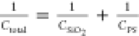 , where Ci is
the capacitance of the dielectric, εs is the static
dielectric constant, k is the Boltzmann constant, d is the thickness of the dielectric, Ctotal is the capacitance of the PS/SiO2 bilayer
film, CSiO2 is the capacitance
of the SiO2 layer, and CPS is
the capacitance. Figure 4c shows the calculated thickness of the modified PS layer deposited
with different concentrations of the PS solution on the SiO2 substrate after spin-coating the C8-BTBT/PMMA blend solution. Interestingly,
due to the dissolution of PS, the resulting thickness of the PS layer
exhibits a small change when the PS concentration is below 120 mg/mL,
which implies that the majority of the PS film has dissolved.
, where Ci is
the capacitance of the dielectric, εs is the static
dielectric constant, k is the Boltzmann constant, d is the thickness of the dielectric, Ctotal is the capacitance of the PS/SiO2 bilayer
film, CSiO2 is the capacitance
of the SiO2 layer, and CPS is
the capacitance. Figure 4c shows the calculated thickness of the modified PS layer deposited
with different concentrations of the PS solution on the SiO2 substrate after spin-coating the C8-BTBT/PMMA blend solution. Interestingly,
due to the dissolution of PS, the resulting thickness of the PS layer
exhibits a small change when the PS concentration is below 120 mg/mL,
which implies that the majority of the PS film has dissolved.
Figure 4.

(a) Measured specific capacitances as a function of frequency for the capacitors using the PS/SiO2 dielectric. (b) Measured specific capacitances as a function of frequency for the capacitors using the PS/SiO2 dielectric after spin-coating the C8-BTBT/PMMA blend solution. The inset is a schematic of the used metal–insulator–metal capacitor structure. (c) Thickness of the PS film deposited with different concentrations of the PS solution on the SiO2 substrate after spin-coating the C8-BTBT/PMMA blend solution.
Figure 5a shows the polarized optical microscopy images of films fabricated by spin-coating the C8-BTBT/PMMA blend solution on the PS layer with different thicknesses. It is found that the domain size becomes larger when the thickness of the PS modification layer increases. When the concentration of the PS solution exceeds 120 mg/mL, the polarized optical contrast of C8-BTBT films becomes weak. Figure 5b,c shows the histograms of mobility and threshold voltage of devices modified with PS films of different thicknesses. The mobilities of the devices increase when the concentration of the PS solution is not higher than 120 mg/mL. However, the mobilities of devices start to decrease when the concentration of the PS solution exceeds 120 mg/mL. When the concentration of the PS solution exceeds 120 mg/mL, an average mobility of >4 cm2/V·s and the highest mobility of >7 cm2/V·s are obtained, which are comparable with those of devices with solution-processed polycrystalline C8-BTBT films and other organic small molecular semiconductors.30,39−43 The deviation in mobility values is slightly large. The possible reason is the defects in C8-BTBT films, different from OTFTs based on polymer semiconductors. The crystallization of the C8-BTBT film is uniform overall, but there are more or less differences in the channel of each device. It can also be seen that the threshold voltages of devices fabricated with PS solutions of different concentrations demonstrate small changes. It is speculated that the thickness of the PS modification layer has little influence on the interface of the semiconductor C8-BTBT and dielectric, but a large influence on the crystallization of C8-BTBT molecules.
Figure 5.

(a) Polarized optical microscopy images of the C8-BTBT/PMMA blend films on SiO2 with different thicknesses of PS films. Histograms of the (b) mobility and (c) threshold voltage of devices modified with different concentrations of the PS solution. All of the blend films are deposited by spin-coating at 5000 rpm.
Figure 6a shows the schematic diagram of the top-contact bottom-gate OFETs with soluble PS layer modification. The threshold voltage is related to materials (semiconductor and dielectric) and traps of the interface of the semiconductor and dielectric. The relatively high threshold may be related to traps resulting from the exposure of the organic semiconductor and/or the organic semiconductor/dielectric interface to the ambient environment in our case. The typical transfer and output characteristics of the device with 120 mg/mL PS modification are shown in Figure 6b,c, respectively. The corresponding dependence of mobility on the gate voltage is shown in Figure S5. The optimized device exhibits a high mobility of 7.01 cm2/V·s and a high on/off ratio of >107. More importantly, devices also demonstrate little hysteresis during the double sweep of the gate voltage. The recently reported characteristics of BG-OFETs based on blends of C8-BTBT and insulating polymers are summarized in Table S2. Although the mobility exceeds 10 cm2/V·s in some OTFTs based on oriented films or single crystals, our devices provide higher competitiveness in C8-BTBT OTFTs based on uniform and isotropous semiconducting films.
Figure 6.

(a) Schematic diagram of the bottom-gate/top-contact OTFTs with 120 mg/mL PS modification. (b) Typical transfer characteristics and (c) output characteristics of C8-BTBT/PMMA blend OTFTs with 120 mg/mL PS modification.
To further understand the influence of soluble insulating polymer modification on the crystallization of C8-BTBT molecules, we also carried out XRD measurements of the C8-BTBT/PMMA blend layer coated on the PS/SiO2 substrate with different thicknesses of PS films. As shown in Figure 7, three characteristic peaks of the (001), (002), and (003) reflections were observed for the films fabricated on the SiO2 substrate with the modification of different thicknesses of PS films. It is clear that the thickness of the PS modification layer largely affects the crystallinity of the C8-BTBT thin film. As is known, the full width at half-maximum (FWHM) of XRD patterns depends on the crystallization of films. The FWHM values of peaks in XRD patterns for the films with the interface modification of PS are extracted. The extracted FWHM values are shown in Table 3. The crystallization of C8-BTBT films will be affected by the dissolved PS modification layer. The dissolved PS amount increases accordingly with the thickness of the PS modification layer. The dissolved bottom PS hinders the aggregation of C8-BTBT, leading to a narrower grain boundary. However, when the dissolved PS amount is very high, C8-BTBT separates to some extent and is hard to concentrate. So, the crystallization of C8-BTBT is weak when 150 mg/mL PS is used, with a correspondingly increased FWHM. The diffraction (001) peak of the film deposited on the substrate with 120 mg/mL PS modification exhibits the smallest FWHM of 0.16°, which implies better crystallization of the C8-BTBT film. This result is consistent with the polarized optical images in Figure 5a. The good crystallization of the C8-BTBT film is attributed to the interface modification of the soluble insulating polymer, which induces the crystallization of C8-BTBT molecules at the soluble polymer interface.
Figure 7.

XRD patterns of C8-BTBT/PMMA blend films deposited on the PS/SiO2 substrate with different thicknesses of PS films.
Table 3. FWHM Values of C8-BTBT/PMMA Blend Films Deposited on the PS/SiO2 Substrate with Different Thicknesses of PS Films.
| PS thickness | 10 mg/mL | 30 mg/mL | 60 mg/mL | 90 mg/mL | 120 mg/mL | 150 mg/mL |
|---|---|---|---|---|---|---|
| FWHM | 0.33° | 0.32° | 0.22° | 0.25° | 0.16° | 0.29° |
Conclusions
In summary, a new method is provided for improving the performances of solution-processed C8-BTBT OTFTs. Highly crystalline, uniform, and isotropic thin films of C8-BTBT were formed by spin-coating a C8-BTBT/PMMA mixture on a substrate with the modification of a soluble polymer film. The excellent crystallization of the semiconductor films is attributed to the interface modification of the soluble insulating polymer, which is beneficial to the crystallization of the small-molecule semiconductor at the interface. As a result, the charge transport is improved and the grain boundary and the domain size of C8-BTBT films are well controlled by adjusting the solubility and thickness of the polymer modification layers. An optimized C8-BTBT OFET with a mobility of >7 cm2/V·s and an on/off ratio of >107 is achieved. Our findings provide a simple and efficient way to modify a small-molecule semiconductor/dielectric interface and to fabricate high-performance OTFTs.
Experimental Section
Materials
The small molecular semiconductor C8-BTBT was purchased from Sigma-Aldrich. Polystyrene (PS, Mw = 3.5 kDa) and poly(methyl methacrylate) (PMMA, Mw = 996 kDa) were purchased from Sigma-Aldrich. Chlorobenzene and butanone solvents were purchased from Sigma-Aldrich. All materials were used as received without further purification.
Preparation of Soluble Polymer Films
Heavily doped p-type silicon wafers with 300 nm-thick SiO2 layers were used as substrates. The Si wafer was used as the gate electrode and the SiO2 layer as the gate insulator. The substrates were ultrasonically cleaned for 15 min with acetone, isopropanol, and DI water. After cleaning, the substrates were placed in an air oven for 30 min at 80 °C to remove residual water. The PS and PMMA solutions with different concentrations in butanone were spin-coated at 3000 rpm for 60 s on SiO2 substrates as the soluble modification layer. The treated wafers were then baked on a 70 °C hot plate for 2 h to remove the residual solvent.
Fabrication of the OFET Devices
C8-BTBT/PMMA blends were prepared by mixing the two components in a 5:1 weight ratio and were dissolved in chlorobenzene to obtain 6 mg/mL solutions. The solutions were further stirred for 1 day to mix completely. The prepared solutions were spin-coated onto soluble polymer films at different speeds in an air environment. Finally, 40 nm-thick Au was deposited to fabricate source and drain electrodes through a metal shadow mask using a thermal evaporator. The channel width/length (W/L) was 2 mm/130 μm.
Characterization
The electrical characteristics of OTFTs were measured using a Keithley 4200 semiconductor analyzer, and the capacitance of soluble polymer films was characterized on an Agilent 4294A. Polarized optical micrographs of C8-BTBT-based films were obtained using a CPV-900 reflectance polarizing microscope. The contact angle of the surface was measured with a video-based automatic contact angle measuring instrument (OCA15, Data Physics). X-ray diffraction (XRD) patterns (2q scans) were obtained using a Bruker Advanced D8 X-ray diffractometer using Cu Kα (λ = 0.154 nm) radiation.
Acknowledgments
This work was financially supported by the National Natural Science Foundation of China (11574075), the Hubei Provincial Department of Science & Technology (2016CFA036), the Hubei Provincial Department of Education (D201602), and the State Key Laboratory of Advanced Technology for Materials Synthesis and Processing (Wuhan University of Technology) (No. 2019-KF-9).
Supporting Information Available
The Supporting Information is available free of charge at https://pubs.acs.org/doi/10.1021/acsomega.0c00548.
AFM images, surface free energy, measured capacitance, the dependence of mobility on gate voltage, and a summary of previously reported work (PDF)
Author Contributions
This paper was written through the contributions of all authors. All authors have given approval to the final version of the paper.
The authors declare no competing financial interest.
Supplementary Material
References
- Li J.; Tang W.; Wang Q.; Sun W.; Zhang Q.; Guo X.; Wang X.; Yan F. Solution-processable organic and hybrid gate dielectrics for printed electronics. Mater. Sci. Eng., R 2018, 127, 1–36. 10.1016/j.mser.2018.02.004. [DOI] [Google Scholar]
- Shaw L.; Bao Z. The Large-Area, Solution-Based Deposition of Single-Crystal Organic Semiconductors. Isr. J. Chem. 2014, 54, 496–512. 10.1002/ijch.201400032. [DOI] [Google Scholar]
- Dong H.; Fu X.; Liu J.; Wang Z.; Hu W. 25th Anniversary Article: Key Points for High-Mobility Organic Field-Effect Transistors. Adv. Mater. 2013, 25, 6158–6183. 10.1002/adma.201302514. [DOI] [PubMed] [Google Scholar]
- Sirringhaus H. 25th anniversary article: organic field-effect transistors: the path beyond amorphous silicon. Adv. Mater. 2014, 26, 1319–1335. 10.1002/adma.201304346. [DOI] [PMC free article] [PubMed] [Google Scholar]
- Li J.; Yan F. Solution-processable low-voltage and flexible floating-gate memories based on an n-type polymer semiconductor and high-k polymer gate dielectrics. ACS Appl. Mater. Interfaces 2014, 6, 12815–12820. 10.1021/am5028007. [DOI] [PubMed] [Google Scholar]
- Li J.; Sun Z.; Yan F. Solution processable low-voltage organic thin film transistors with high-k relaxor ferroelectric polymer as gate insulator. Adv. Mater. 2012, 24, 88–93. 10.1002/adma.201103542. [DOI] [PubMed] [Google Scholar]
- Jiang L.; Liu J.; Lu X.; Fu L.; Shi Y.; Zhang J.; Zhang X.; Geng H.; Hu Y.; Dong H.; et al. Controllable growth of C 8-BTBT single crystalline microribbon arrays by a limited solvent vapor-assisted crystallization (LSVC) method. J. Mater. Chem. C 2018, 6, 2419–2423. 10.1039/C8TC00447A. [DOI] [Google Scholar]
- Li H.; Tee B. C.; Cha J. J.; Cui Y.; Chung J. W.; Lee S. Y.; Bao Z. High-mobility field-effect transistors from large-area solution-grown aligned C60 single crystals. J. Am. Chem. Soc. 2012, 134, 2760–2765. 10.1021/ja210430b. [DOI] [PubMed] [Google Scholar]
- Chai Z.; Abbasi S. A.; Busnaina A. A. Scalable Directed Assembly of Highly Crystalline 2, 7-Dioctyl [1] benzothieno [3, 2-b][1] benzothiophene (C8-BTBT) Films. ACS Appl. Mater. Interfaces 2018, 10, 18123–18130. 10.1021/acsami.8b01433. [DOI] [PubMed] [Google Scholar]
- Kang B.; Ge F.; Qiu L.; Cho K. Effective Use of Electrically Insulating Units in Organic Semiconductor Thin Films for High-Performance Organic Transistors. Adv. Electron. Mater. 2017, 3, 1600240 10.1002/aelm.201600240. [DOI] [Google Scholar]
- Liu C.; Li Y.; Lee M. V.; Kumatani A.; Tsukagoshi K. Self-assembly of semiconductor/insulator interfaces in one-step spin-coating: a versatile approach for organic field-effect transistors. Phys. Chem. Chem. Phys. 2013, 15, 7917–7933. 10.1039/c3cp44715d. [DOI] [PubMed] [Google Scholar]
- Smith J.; Hamilton R.; McCulloch I.; Stingelin-Stutzmann N.; Heeney M.; Bradley D. D.; Anthopoulos T. D. Solution-processed organic transistors based on semiconducting blends. J. Mater. Chem. 2010, 20, 2562–2574. 10.1039/b921674j. [DOI] [Google Scholar]
- Kang M.; Hwang H.; Park W.-T.; Khim D.; Yeo J.-S.; Kim Y.; Kim Y.-J.; Noh Y.-Y.; Kim D.-Y. Ambipolar Small-Molecule: Polymer Blend Semiconductors for Solution-Processable Organic Field-Effect Transistors. ACS Appl. Mater. Interfaces 2017, 9, 2686–2692. 10.1021/acsami.6b12328. [DOI] [PubMed] [Google Scholar]
- Ford M. J.; Wang M.; Patel S. N.; Phan H.; Segalman R. A.; Nguyen T.-Q.; Bazan G. C. High mobility organic field-effect transistors from majority insulator blends. Chem. Mater. 2016, 28, 1256–1260. 10.1021/acs.chemmater.5b04774. [DOI] [Google Scholar]
- Park M.; Min Y.; Lee Y. J.; Jeong U. Growth of Long Triisopropylsilylethynyl Pentacene (TIPS-PEN) Nanofibrils in a Polymer Thin Film During Spin-Coating. Macromol. Rapid Commun. 2014, 35, 655–660. 10.1002/marc.201300837. [DOI] [PubMed] [Google Scholar]
- Park B.; Jeon H. G.; Choi J.; Kim Y.; Lim J.; Jung J.; Cho S. Y.; Lee C. High-performance organic thin-film transistors with polymer-blended small-molecular semiconductor films, fabricated using a pre-metered coating process. J. Mater. Chem. 2012, 22, 5641–5646. 10.1039/c2jm16007b. [DOI] [Google Scholar]
- Naden A. B.; Loos J.; MacLaren D. A. Structure–function relations in diF-TES-ADT blend organic field effect transistors studied by scanning probe microscopy. J. Mater. Chem. C 2014, 2, 245–255. 10.1039/C3TC31783H. [DOI] [Google Scholar]
- Zhong H.; Smith J.; Rossbauer S.; White A. J. P.; Anthopoulos T. D.; Heeney M. Air-Stable and High-Mobility n-Channel Organic Transistors Based on Small-Molecule/Polymer Semiconducting Blends. Adv. Mater. 2012, 24, 3205–3211. 10.1002/adma.201200859. [DOI] [PubMed] [Google Scholar]
- Hwang D. K.; Fuentes-Hernandez C.; Berrigan J. D.; Fang Y.; Kim J.; Potscavage W. J.; Cheun H.; Sandhage K. H.; Kippelen B. Solvent and polymer matrix effects on TIPS-pentacene/polymer blend organic field-effect transistors. J. Mater. Chem. 2012, 22, 5531–5537. 10.1039/c2jm16487f. [DOI] [Google Scholar]
- Ohe T.; Kuribayashi M.; Yasuda R.; Tsuboi A.; Nomoto K.; Satori K.; Itabashi M.; Kasahara J. Solution-processed organic thin-film transistors with vertical nanophase separation. Appl. Phys. Lett. 2008, 93, 053303 10.1063/1.2966350. [DOI] [Google Scholar]
- Li X.; Smaal W. T.; Kjellander C.; Van Der Putten B.; Gualandris K.; Smits E. C.; Anthony J.; Broer D. J.; Blom P. W.; Genoe J.; Gelinck G. Charge transport in high-performance ink-jet printed single-droplet organic transistors based on a silylethynyl substituted pentacene/insulating polymer blend. Org. Electron. 2011, 12, 1319–1327. 10.1016/j.orgel.2011.04.020. [DOI] [Google Scholar]
- Galindo S.; Tamayo A.; Leonardi F.; Mas-Torrent M. Control of Polymorphism and Morphology in Solution Sheared Organic Field-Effect Transistors. Adv. Funct. Mater. 2017, 27, 1700526 10.1002/adfm.201700526. [DOI] [Google Scholar]
- Lee W. H.; Kwak D.; Anthony J. E.; Lee H. S.; Choi H. H.; Kim D. H.; Lee S. G.; Cho K. The Influence of the Solvent Evaporation Rate on the Phase Separation and Electrical Performances of Soluble Acene-Polymer Blend Semiconductors. Adv. Funct. Mater. 2012, 22, 267–281. 10.1002/adfm.201101159. [DOI] [Google Scholar]
- Smith J.; Hamilton R.; Qi Y.; Kahn A.; Bradley D. D. C.; Heeney M.; McCulloch I.; Anthopoulos T. D. The Influence of Film Morphology in High-Mobility Small-Molecule: Polymer Blend Organic Transistors. Adv. Funct. Mater. 2010, 20, 2330–2337. 10.1002/adfm.201000427. [DOI] [Google Scholar]
- Huang Y.; Sun J.; Zhang J.; Wang S.; Huang H.; Zhang J.; Yan D.; Gao Y.; Yang J. Controllable thin-film morphology and structure for 2, 7-dioctyl [1] benzothieno [3, 2-b][1] benzothiophene (C8BTBT) based organic field-effect transistors. Org. Electron. 2016, 36, 73–81. 10.1016/j.orgel.2016.05.019. [DOI] [Google Scholar]
- Lee S. G.; Lee H. S.; Lee S.; Kim C. W.; Lee W. H. Thickness-dependent electrical properties of soluble acene–polymer blend semiconductors. Org. Electron. 2015, 24, 113–119. 10.1016/j.orgel.2015.05.030. [DOI] [Google Scholar]
- Hamaguchi A.; Negishi T.; Kimura Y.; Ikeda Y.; Takimiya K.; Bisri S. Z.; Iwasa Y.; Shiro T. Single-Crystal-Like Organic Thin-Film Transistors Fabricated from Dinaphtho [2, 3-b: 2′, 3′-f] thieno [3, 2-b] thiophene (DNTT) Precursor–Polystyrene Blends. Adv. Mater. 2015, 27, 6606–6611. 10.1002/adma.201502413. [DOI] [PubMed] [Google Scholar]
- Ljubic D.; Jarvis V.; Smithson C. S.; Hu N.-X.; Wu Y.; Zhu S. Effects of gate dielectric surface modification on phototransistors with polymer-blended benzothieno [2, 3-b] benzothiophene semiconductor thin films. Org. Electron. 2017, 44, 253–262. 10.1016/j.orgel.2017.02.027. [DOI] [Google Scholar]
- Ljubic D.; Smithson C. S.; Wu Y.; Zhu S. Highly UV-Sensitive and Responsive Benzothiophene/Dielectric Polymer Blend-Based Organic Thin-Film Phototransistor. Adv. Electron. Mater. 2015, 1, 1500119 10.1002/aelm.201500119. [DOI] [Google Scholar]
- Wei W.; Yang C.; Mai J.; Gong Y.; Yan L.; Zhao K.; Ning H.; Wu S.; Gao J.; Gao X.; et al. High mobility solution-processed C 8-BTBT organic thin-film transistors via UV-ozone interface modification. J. Mater. Chem. C 2017, 5, 10652–10659. 10.1039/C7TC03794E. [DOI] [Google Scholar]
- Feng X.; Wang Y.; Lin G.; Wang X.; Wang X.; Zhang G.; Lu H.; Qiu L. Improving performance of selective-dewetting patterned organic transistors via semiconductor-dielectric blends. Synth. Met. 2014, 194, 59–64. 10.1016/j.synthmet.2014.04.017. [DOI] [Google Scholar]
- Li Y.; Liu C.; Wang Y.; Yang Y.; Wang X.; Shi Y.; Tsukagoshi K. Flexible field-effect transistor arrays with patterned solution-processed organic crystals. AIP Adv. 2013, 3, 052123 10.1063/1.4807669. [DOI] [Google Scholar]
- Kjellander B. C.; Smaal W. T.; Anthony J. E.; Gelinck G. H. Inkjet Printing of TIPS-PEN on Soluble Polymer Insulating Films: A Route to High-Performance Thin-Film Transistors. Adv. Mater. 2010, 22, 4612–4616. 10.1002/adma.201001697. [DOI] [PubMed] [Google Scholar]
- Yoo H.; Choi H. H.; Shin T. J.; Rim T.; Cho K.; Jung S.; Kim J. J. Self-Assembled, Millimeter-Sized TIPS-Pentacene Spherulites Grown on Partially Crosslinked Polymer Gate Dielectric. Adv. Funct. Mater. 2015, 25, 3658–3665. 10.1002/adfm.201501381. [DOI] [Google Scholar]
- Paterson A. F.; Tsetseris L.; Li R.; Basu A.; Faber H.; Emwas A.-H.; Panidi J.; Fei Z.; Niazi M. R.; Anjum D. H.; Heeney M.; Anthopoulos T. D. Addition of the Lewis Acid Zn(C6F5)2 Enables Organic Transistors with a Maximum Hole Mobility in Excess of 20 cm2 V–1 s–1. Adv. Mater. 2019, 31, 1900871 10.1002/adma.201900871. [DOI] [PubMed] [Google Scholar]
- Yuan Y.; Giri G.; Ayzner A. L.; Zoombelt A. P.; Mannsfeld S. C.; Chen J.; Nordlund D.; Toney M. F.; Huang J.; Bao Z. Ultra-high mobility transparent organic thin film transistors grown by an off-centre spin-coating method. Nat. Commun. 2014, 5, 3005 10.1038/ncomms4005. [DOI] [PubMed] [Google Scholar]
- Liu C.; Minari T.; Lu X.; Kumatani A.; Takimiya K.; Tsukagoshi K. Solution-processable organic single crystals with bandlike transport in field-effect transistors. Adv. Mater. 2011, 23, 523–526. 10.1002/adma.201002682. [DOI] [PubMed] [Google Scholar]
- Jiang C.; Choi H. W.; Cheng X.; Ma H.; Hasko D.; Nathan A. Printed subthreshold organic transistors operating at high gain and ultralow power. Science 2019, 363, 719–723. 10.1126/science.aav7057. [DOI] [PubMed] [Google Scholar]
- Hunter S.; Chen J.; Anthopoulos T. D. Microstructural Control of Charge Transport in Organic Blend Thin-Film Transistors. Adv. Funct. Mater. 2014, 24, 5969–5976. 10.1002/adfm.201401087. [DOI] [Google Scholar]
- Li Y.; Liu C.; Xu Y.; Minari T.; Darmawan P.; Tsukagoshi K. Solution-processed organic crystals for field-effect transistor arrays with smooth semiconductor/dielectric interface on paper substrates. Org. Electron. 2012, 13, 815–819. 10.1016/j.orgel.2012.01.021. [DOI] [Google Scholar]
- Choi J.; Jeon H. G.; Kwon O. E.; Bae I.; Cho J.; Kim Y.; Park B. Improved output characteristics of organic thin film transistors by using an insulator/protein overlayer and their applications. J. Mater. Chem. C 2015, 3, 2603–2613. 10.1039/C4TC02823F. [DOI] [Google Scholar]
- Raghuwanshi V.; Bharti D.; Mahato A. K.; Varun I.; Tiwari S. P. Solution-Processed Organic Field-Effect Transistors with High Performance and Stability on Paper Substrates. ACS Appl. Mater. Interfaces 2019, 11, 8357–8364. 10.1021/acsami.8b21404. [DOI] [PubMed] [Google Scholar]
- Pérez-Rodríguez A.; Temiño I.; Ocal C.; Mas-Torrent M.; Barrena E. Decoding the Vertical Phase Separation and Its Impact on C8-BTBT/PS Transistor Properties. ACS Appl. Mater. Interfaces 2018, 10, 7296–7303. 10.1021/acsami.7b19279. [DOI] [PubMed] [Google Scholar]
Associated Data
This section collects any data citations, data availability statements, or supplementary materials included in this article.