Abstract
In this paper, we describe how PolyJet 3D printing technology can be used to fully integrate electrode materials into microfluidic devices during the print process. This approach uses stacked printing (separate printing steps and stage drops) with liquid support to result in devices where electrodes and a capillary fluidic connection are directly integrated and ready to use when printing is complete. A key feature of this approach is the ability to directly incorporate electrode materials into the print process so that the electrode(s) can be placed anywhere in the channel (at any height). We show that this can be done with a single electrode or an electrode array (which led to increases in signal). In both cases, we found that a middle electrode configuration leads to a significant increase in the sensitivity, as opposed to more traditional bottom channel placement. Since the electrode is embedded in the device, in situ platinum black deposition was performed to aid in the detection of nitric oxide. Finally, a generator-collector configuration with an opposed counter electrode was made by placing two working electrodes ~750 μm apart (in the middle of the channel) and a platinum counter electrode at the bottom of the channel. The utility of this configuration was demonstrated by dual electrode detection of catechol. This 3D printing approach affords robust electrochemical detection schemes with new electrode configurations being possible in a manner that also increases the ease of use and transferability of the 3D printed devices with integrated electrode materials.
Introduction
Since the 1990s, research in the area Lab on a Chip (LOC) technology has included work on developing a total analysis system with integrated functions such as sample preparation and detection along with analytical assays such as PCR and separations.1–4 One logical detection scheme for this type of total integration is electrochemical detection. Electrodes can be made as large or a small as necessary (cm-nm scales) making them easy to incorporate into a variety of fluidic devices.5–8 The data acquisition systems for electrochemical systems (potentiostats) have been consistently shrinking for the last two decades, with systems as small as 27 mm × 20 mm and using as little as 3.7 V being possible.9–11
Integration of electrodes into a fluidic chip can vary based upon the substrate type and the desired electrode configuration. One of the earliest examples of integrating electrodes in microfluidic device is by Woolley et al.12 The approach used a glass-based electrophoresis chip with patterned Pt working and counter electrodes (made with sputtering and lithographic patterning). The device was used for the separation and detection of various neurotransmitters and DNA.12 Since Woolley et al.’s first demonstration, several other techniques have arisen for integrating electrodes in microfluidic networks. Solution, sputter, and paste-based electrode approaches have been used along with patterning techniques such as lithography to produce defined electrodes out of various materials.13–17 While a wide range of electrode materials can be used there can be complexity in the fabrication. For example, in the original work by Woolley et al. the device was made from glass and the fabrication required photolithography, plasma sputtering, drilling, wet chemical etching, and thermal bonding steps.12 The bonding process has been simplified by utilizing glass-PDMS hybrid devices, with reversible or irreversible (after plasma treatment) bonding.7 These types of devices generally use similar processes for electrode fabrication but avoid glass etching of channel features by using soft lithography techniques.18 More recently, thermoplastic-PDMS devices have been fabricated that embed electrode materials in a polystyrene base, which can be polished to expose the electrode surface (and bonded to a), PDMS structure.19, 20 These methods present options for the direct incorporation of electrodes into microfluidic networks; however, each of these techniques require access to fabrication facilities and complex multi-step procedures. This complexity leads to limitations in accessibility to non-experts and scale-up of production.
An appealing alternative to these complex fabrication methods is the rapid manufacturing capabilities found in 3D printing. The use of 3D printing of fluidic devices is relatively new, with the first example of electrode incorporation in such devices occurring in 2014.5, 21, 22 Erkal et al. were able to embed electrode materials in commercially available PEEK fittings by packing the fitting with an epoxy resin around the electrode materials.5 The fitting could then be polished to expose a flat electrode surface and then threaded into a 3D printed device. This screw-in type design has been adopted by several groups, however there is a manual nature to electrode fabrication and incorporation as well as issues in placing multiple electrodes within a small area.23, 24 Additionally, the size of the PEEK fitting limits how closely separate electrodes can be placed (for devices where multiple electrodes is desired) as well as how close inlet and outlet ports can be placed within a device (relative to the electrodes). The PEEK (electrode) fitting size also can lead to dead volume issues.5 This electrode/fitting approach has been mainly utilized in devices produced by higher resolution, resin-based 3D printing technologies (such as PolyJet or Stereolithography) but there have been reports of Fused Deposition Modeling (FDM)-based devices that incorporate printable electrodes.25, 26 These techniques require the use of carbon doped filaments.
Recently, the realization that 3D printing can be further enhanced by the incorporation of non 3D printed materials has been explored by several groups.27 Here, we report the use of a PolyJet 3D printing technology for the direct incorporation of electrode materials into the printed devices. This process uses stacked printing (separate printing steps), stage drops, and liquid support to result in devices where electrodes and capillary are directly integrated and ready to use when printing is complete. PolyJet technology is preferred in this application for two reasons. First, the technique is high resolution allowing for sub-mm channel dimensions.28 Second, the material is applied as a liquid that is then cured into a hard plastic. This allows the embedded electrode material to be firmly encased in the plastic, leading to a leak-free seal. A key feature of this approach is the ability to directly incorporate electrode materials into the print process so that the electrode(s) can be placed anywhere in the channel (at any height). Fluidic connections are made easy by directly embedding capillaries into the printed device as part of the process. It is also shown that multiple working electrodes can be integrated together (for dual electrode experiments) along with other electrodes such as a counter electrode, resulting in a totally integrated device. This approach simplifies fabrication processes while also increasing the ease of use and transferability of the 3D printed devices with integrated electrode materials.
Experimental
Materials and Chemicals
Parallel bar gold TEM grids (100 mesh, 3 mm) were obtained from SPI supplies (West Chester, PA). Fused-silica capillary (150 μm ID × 360 μm OD) was purchased from Polymicro Technologies (Phoenix, AZ). Catechol, glycerol, and platinum foil (thickness 0.025 mm, 99.9%) were both obtained from Millipore-Sigma (St. Louis, MO). Phosphate-buffered saline solution (10X, pH 7.4) and isopropyl alcohol were obtained from Thermo-Fisher Scientific (St. Louis, MO). Permatex 84101 5-minute epoxy was purchased from Permatex (Solon, OH). High conductivity silver epoxy 8330 was purchased from MG Chemicals (Ontario, Canada). Platinum wire (250 μm) was purchased from Alfa Aesar (Ward Hill, MA)
Device Fabrication via Stacked Printing
The devices described in this paper were designed using Autodesk Inventor Professional 2020 (Autodesk Inventor, San Rafael, CA) and exported into .STL format for printing. Special design considerations were made for the devices in order to not utilize conventional support materials and to allow the placement of electrode materials during the print process. In short, three separate models (base model, channel model, cover model) were designed to complete a single device, where the models are separate prints that are combined to create the final device. We term this a stacked-print process. Depending on where the electrode is being placed within the channel (376 × 376 μm): bottom of the channel (Figure 3A) or middle of the channel (Figure 3B), part of the channel is broken into a base model and a channel model (middle device), or as residing solely in the channel model (bottom device).
Figure 3.
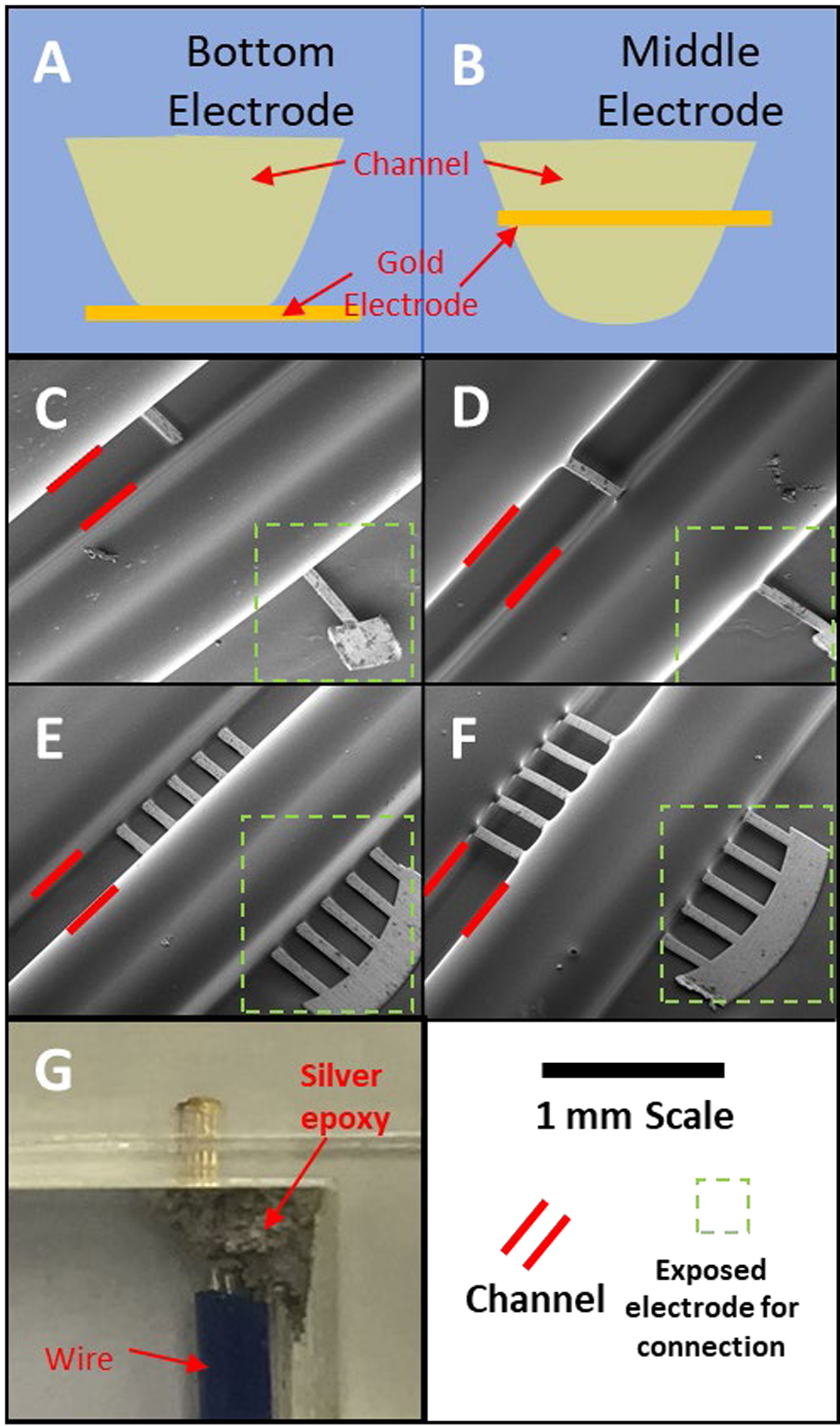
Various electrode configurations that were explored. (A) schematic representation of electrode at the bottom of the channel as compared to (B), which shows the electrode placed in the middle of the channel. (C) and (D) contain SEM images of a single gold post (65 μm wide) cut from a TEM grid embedded at the bottom (C) and the middle (D) of the channel. (E) and (F) have SEM images of five post (each 65 μm wide) electrode array (175 μm spacing) in the bottom (E) and the middle (F) of the channel. For clarity, in each image the channel is outlined by two red lines and electrode connection area is defined by a green dashed box. (G) Optical image of the electrode array embedded at the bottom of the channel.
Settings were adjusted on an Eden 260V PolyJet 3D printer such that support material is not utilized in the print, similar to what was reported previously.28 For the middle electrode device (Figure 1) the .STL file for the bottom model was printed to half of the desired channel height (188 μm) and a 3 mm circle, recessed 30 μm from the top of the model, was printed to guide the electrode placement (Figure 1A). The electrode was placed in the device with the guide and the starting position of the Z-axis was lowered by the height of the previous print (Figure 1B). The channel model, containing the remainder of the channel (188 μm), was printed directly on top of the base model enclosing the electrode (Figure 1C). After completion of the channel model, a small amount of 5-minute epoxy was placed at the end of the channel to adhere ~2 cm of a 7 cm long capillary into the capillary side of the device (Figure 1D), with excess epoxy being removed with a PDMS squeegee. The remainder of the channel was filled with a 65:35 (w/w) glycerol/isopropanol solution to serve as the liquid support.28 Excess solution was removed with a PDMS squeegee. The Z-axis start position was dropped by the height of the channel model and then the cover model was printed directly on top of the channel model (Figure 1E, this process is also outlined with a video in the supplemental information). Once completed, the device was removed from the print tray, and the liquid support was removed by flushing with DI water, IPA, and then electrolyte solution. Electrical connection was made to the exposed portion of the electrode in two ways: a flat alligator clip was clipped directly to the electrode or with silver conductive two-part epoxy (MG Chemicals 8330TCS). The bottom electrode device as well as the dual working electrode with embedded counter electrode were fabricated utilizing the same process, with the device being cut into different models depending on the electrode placement (Figure S1 and S2).
Figure 1.
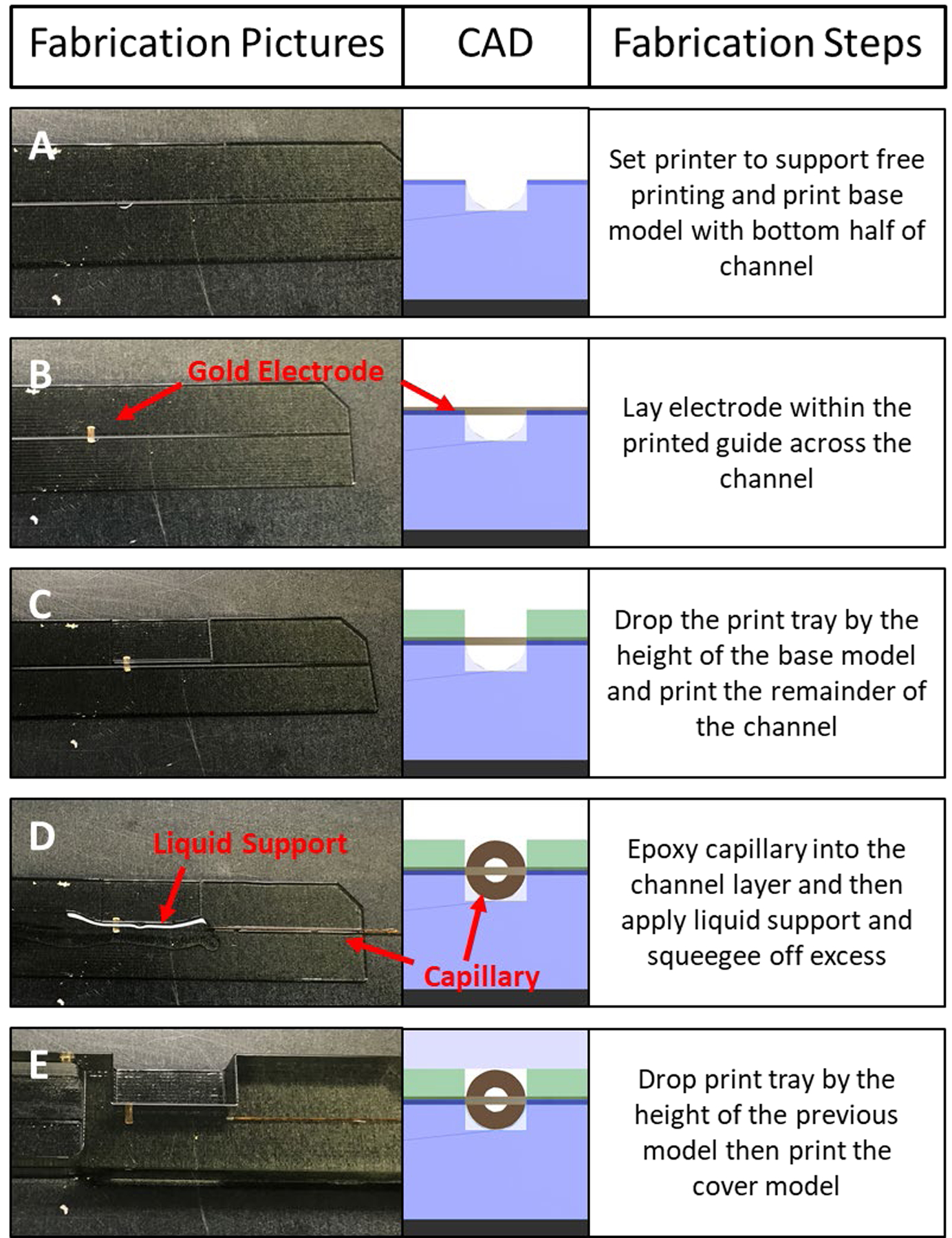
Step-by-step process of making a 3D printed device with an embedded gold electrode placed in the middle of the channel. Left column contains pictures of various points of the print process, the center column is the cross-sectional CAD rendering of each step, and the right column has text explaining the process. In (A) the printer is set to print without a support pedestal and the base layer is printed to half of the channel height. Before printing stops, a 30 μm recessed guide for the electrode is printed. In (B) the gold electrode is placed within the guide and the start position of the z-axis is dropped by the height of the print before printing resumes. (C) The channel layer is printed directly on top of the electrode and base layer. This seals the electrode into the printed plastic. (D) A small amount of 5 min two-part epoxy is used to coat a 360 um o.d. capillary before it is placed into the device. Then a mixture of glycerol and isopropanol liquid support (65:35 v:v) is applied to the channel and the excess is removed by a PDMS squeegee. (E) Finally, the z-axis start position is dropped by the height of the channel layer and the cover layer is printed directly on the previous layer, sealing in the liquid support and the capillary. After printing, the liquid support is removed by flushing with isopropanol.
Characterization
Optical images of the various devices were taken using a SZ16 Stereomicroscope (Olympus) equipped with an Infinity 2 CCD camera (Lumenera). Computer tomography (CT) scans were obtained on a MicroCT 35, ScanCo Medical, Brüttisellen, Switzerland. The following conditions were used: X-ray tube potential 70 kVp, integration time 300 ms, X-ray intensity 145 μA, isotropic voxel size 12 um, frame averaging 1, projections 500, medium resolution scan. CT scans were converted to DIACOM format and segmented in Mimics Research V21.0 (Materialise). Scanning electron micrographs were acquired on a FEI Inspect F using a10 kV applied voltage, spot size of 1.0, working distance of 10.5 mm, and a dwell time of 3 μs.
Amperometric Detection of Catechol
With the embedded gold working electrode, a three-electrode system was utilized, with a Ag/AgCl reference electrode and a 250 μm platinum wire auxiliary electrode being placed in the reservoir at the channel exit. Amperometric detection of catechol was completed for all devices using the Amperometric i-t Curve technique in the CH1812C program. The voltage was fixed at +0.9 V vs Ag/AgCl for oxidative analysis. All catechol solutions, buffer, isopropanol (IPA), and water were filtered with 0.22 μm syringe filters (Fisherbrand, St. Louis, MO) before they were used in the device. Samples ranging from 0.2 −12.5 μM were made from a 7.45 mM catechol stock solution and diluted with PBS. A 1 mL gastight syringe was used to flow PBS buffer into the device. This syringe was connected to a 4-port valve (Valco Instruments Co. Inc., Houston, TX) with a 1 μL internal rotor by using capillary tubing with a NanoTight Tubing Sleeves (IDEX). The 3D-microfluidic device was connected to the system by another NanoTight Tubing Sleeve and an in-line filter in place before the device. The flow was controlled at 10 μL/min via syringe pump (Harvard Apparatus, Holliston, MA). Analysis of catechol was performed starting with a PBS blank and working up in concentration (0.1 – 12.5 μM).
Nitric Oxide Detection
The gold electrode array was coated with platinum black in situ using a 35% H2Cl6Pt, 0.005% C4H6O4Pb solution and voltammogram-based deposition step. The cyclic voltammogram was run from +0.6 to −0.35 V vs Ag/AgCl and scan rate of 0.02 V/s. Nitric oxide (NO) standards were prepared fresh as needed by deoxygenating PBS with Ar (Airgas) for 30 minutes then purging with NO gas (99.5%, Airgas) for 30 minutes to yield a 1.9 mM NO stock solution. The NO gas was purified by passing through a packed KOH column. Standards were then diluted with PBS (into de-gassed flasks) to result in concentrations between 0.15 – 38 μM. The other experimental conditions were the same as with catechol detection.
Generator-Collector Detection of Catechol
Dual-electrode, generator-collector detection of catechol (and the subsequent quinone) was performed using a device with two embedded gold arrays (placed in the middle of the channel) and an embedded platinum foil (cut to be 5 × 3 mm in width, 0.025 mm thickness) to act as a counter electrode (at the bottom of the channel, directly opposing the working electrodes). The flow experimental set up was the same as described for the above catechol experiments A CHI812b bi-potentiostat was used for data collection. The catechol was oxidized at the first electrode array at a potential of +0.80 V vs Pt and the quinone product reduced at the second array at −0.25 V. Standards of catechol were prepared in PBS in concentrations ranging from 2.5 – 10 μM.
Results and Discussion
Below we describe this new method for directly incorporating electrode materials and fused silica capillaries into a PolyJet 3D printing process that does not use solid support material. The fabrication process for embedded electrodes and capillaries is shown in Figures 1 (for middle of the channel electrode placement, also outlined with a video in the supplemental information), S1 (for bottom of the channel electrode placement), and S2 (for electrode placement in both the bottom and middle of the channel, in the same device). This process relies on two key techniques. The first is the ability to use liquid support (65:35 glycerol-IPA) so the electrode materials are not contaminated during the printing process and solid supports do not have to be manually removed from small channels.28 The second is the ability of 3D printing technology to perform stacked prints, which allows the user to easily embed non-3D printed materials at specific locations within a device. In short, stack printing is where the user prints a model onto the tray, leaves it on the tray and resets the z-axis start position to the height of the finished model. If one desires to embed a material (in this case adding the electrode to the device), the user can add it to the print, drop the start position of the stage, and then print a new model directly on top of the previous model. A stacked print approach is required with PolyJet technology because slicer programs do not allow the user to explicitly dictate pause points in the print or support material placement. By stacking prints the user has more control over the placement of foreign objects into the print and full understanding of where the slicer will place support materials.
To simplify the world-to-chip fluidic connection, fused silica capillary (360 μm o.d.) can be directly incorporated into the 3D printed device (Figure 1D). To accomplish this, a channel (designed to be 376 × 376 μm) was used to accommodate the capillary outer diameter. These dimensions resulted in a snug but not perfect fit of the capillary in the channel. In order to ensure a liquid tight seal, a small amount of 5-minute epoxy is coated around the capillary when it is placed in the channel. Figure 2A shows the connection in an actual device. To characterize this connection, micro-computed tomography (μCT) was used, with the μCT rendering being shown in Figures 2B & 2C. These renderings show the capillary (blue) is center within the channel structure (yellow). The void space seen around the capillary in Figure 2C illustrates the need for the epoxy when embedding in the device.
Figure 2.
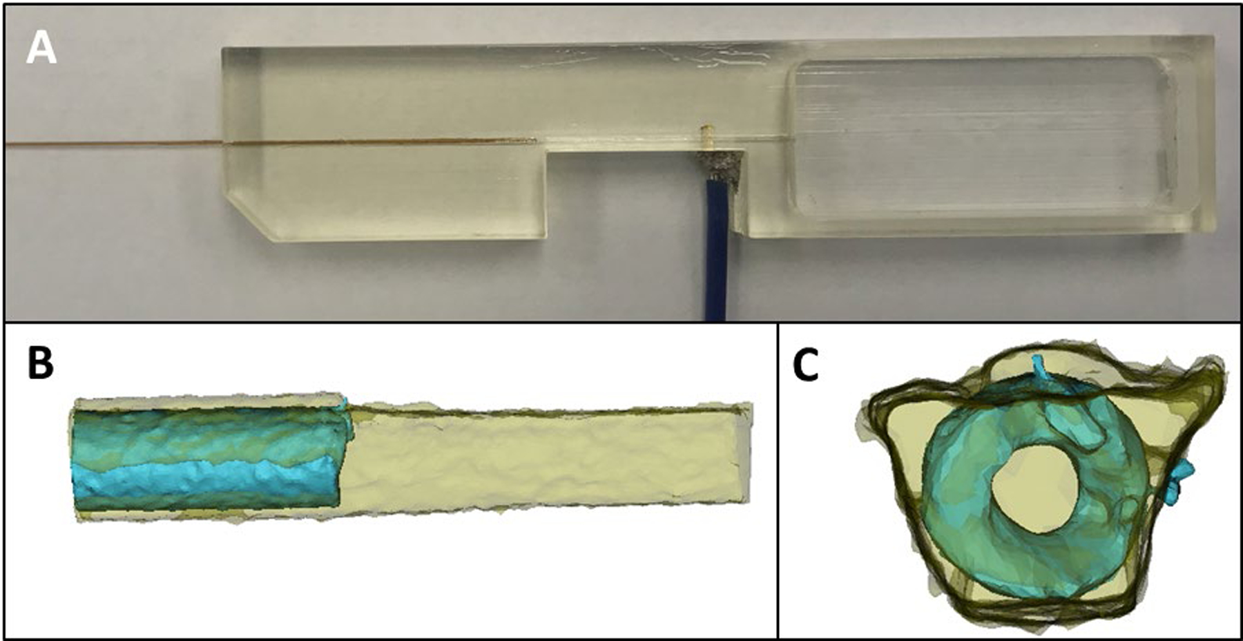
Characterization of capillary placement in the 3D printed device. (A) Optical image of the device containing both a capillary and electrode array. (B) and (C) are CT renderings of the capillary/channel interface. (B) is the side view and (C) is the head on view, showing that the capillary is centered within the channel.
The ability to stack print and embed materials as desired during the process allowed us to explore the ability to position the electrode in various points in the channel. Liu et al. were able to see a signal enhancement by placing a wire electrode across the channel in a PDMS device.29 They theorized that the signal enhancement came from the ability of the solution to flow around the electrode. One key advantage of the 3D printing approach presented here is the ability to precisely and reproducibly place the electrode at any height within the channel. Figure 3 shows the two configurations that were explored in this study, either the bottom of the channel (Figure 3A) or the middle of the channel (Figure 3B). In traditionally fabricated devices, thin-layer electrodes that are at the bottom of the fluidic channel is the standard.30, 31 The ability to have electrodes elsewhere in the channel structure including the middle of the channel, where all sides of the electrode come into contact with the fluid, is unique to this 3D printing method. In addition to spatially locating the electrodes in the channel, the sensitivity could be enhanced by using an array of electrodes, which was enabled here by using more posts from the TEM grid that was embedded.32 In order to characterize how the electrode materials are embedded during the 3D printing process, devices without the cover model were printed with either a single electrode (65 μm wide) or five-electrode array (each 65 μm wide, spacing of 175 μm) and imaged with scanning electrode microscopy. This led to four configurations to explore: Single electrode at the bottom of the channel (Figure 3C), single electrode at the middle of the channel (Figure 3D), 5-electrode array at the bottom of the channel (Figure 3E), 5-electrode array at the middle of the channel (Figure 3F). The key feature shown in these images are the small dimples of material surrounding the electrode. Since the 3D printing material is a liquid when it is jetted, it seals around the thin electrode material before it is cured, hardening (upon exposure to UV light) to form a liquid tight seal. In the bottom right hand corner of each SEM image the exposed region of the electrode can be seen in which electrical contact could be made to the potentiostat (outlined with dotted box). Electrical contact was made utilizing two-part silver conductive epoxy to attach copper wire to the electrodes (Figure 3G).
Figure 4 shows the results of changing electrode size and placement within the fluidic channel. Figure 4A shows a peak overlay of each configuration resulting from a 1 μL injection of a 3 μM catechol solution. The figure shows that as the surface area increases from a single electrode to a 5-electrode array, peak area increases (as expected). Secondly, as compared to the bottom electrode placement, the middle of the channel electrode placement results in the analyte accessing more electrode area and subsequently a signal enhancement reflected by an increase in the calibration sensitivity (slope of the calibration curve, see Figure 4B). As can be seen, moving the electrode placement from the bottom of the channel (traditional placement) to the middle of the channel results in a 2.3-fold increase in sensitivity (for the 5-electrode array comparison). In addition, the ability to move from a single electrode to a 5-electrode array leads to 4.9-fold increase in sensitivity for the middle channel placement. A similar improvement in the limit of detection (LOD) for catechol was also seen, with a LOD of 275 nM with a single electrode in the middle of the channel and 55 nM for a 5-electrode array placed in the middle of the channel. These detection limits for catechol are similar to other non 3D printed microfluidic flow cells using amperometric detection.26, 33, 34
Figure 4.
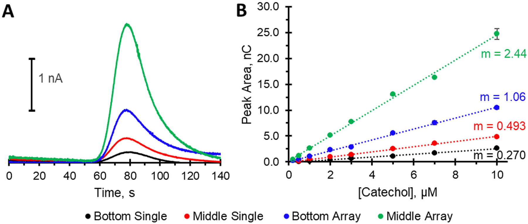
Effect of electrode placement and number for the amperometric detection of a 3 μM catechol solution. (A) Overlay of single electrode response for bottom or middle placement as well as 5 array electrode response for bottom or middle placement. (B) Calibration curves of catechol for each condition in (A), showing the enhanced sensitivity gained by moving to a 5-post array placed in the center of the channel (r2 ≥ 0.9954).
Nitric oxide (NO) is a challenging analyte for flow based electrochemical analysis. It is a key player in biological processes such as vasodilation and inflammation, it has a short half-life (on the order of seconds due to its reaction with oxygen), and nM detection limits are often required.5, 35 One advantage of the devices described here for NO detection is the limited gas permeability of Polyjet materials.36 Since platinum black electrodes have been shown to further enhance the sensitivity of NO detection,35 in situ platinum black deposition was performed on the gold array (middle channel placement, each 65 μm wide with a 175 μm spacing). Figure 5A shows the effect of this platinum black deposition. The black coating can clearly be seen inside of the channel area whereas outside the channel still shows as gold. Figure 5B shows the resulting detection of NO with the platinum black coated gold array (replicate injections of 38.0, 28.5, and 19.0 μM NO is shown), with a full calibration curve shown in Figure S3. This setup resulted in a limit of detection of 45 nM for NO, which is comparable to other Pt-black electrode results in microfluidic devices35,37
Figure 5.
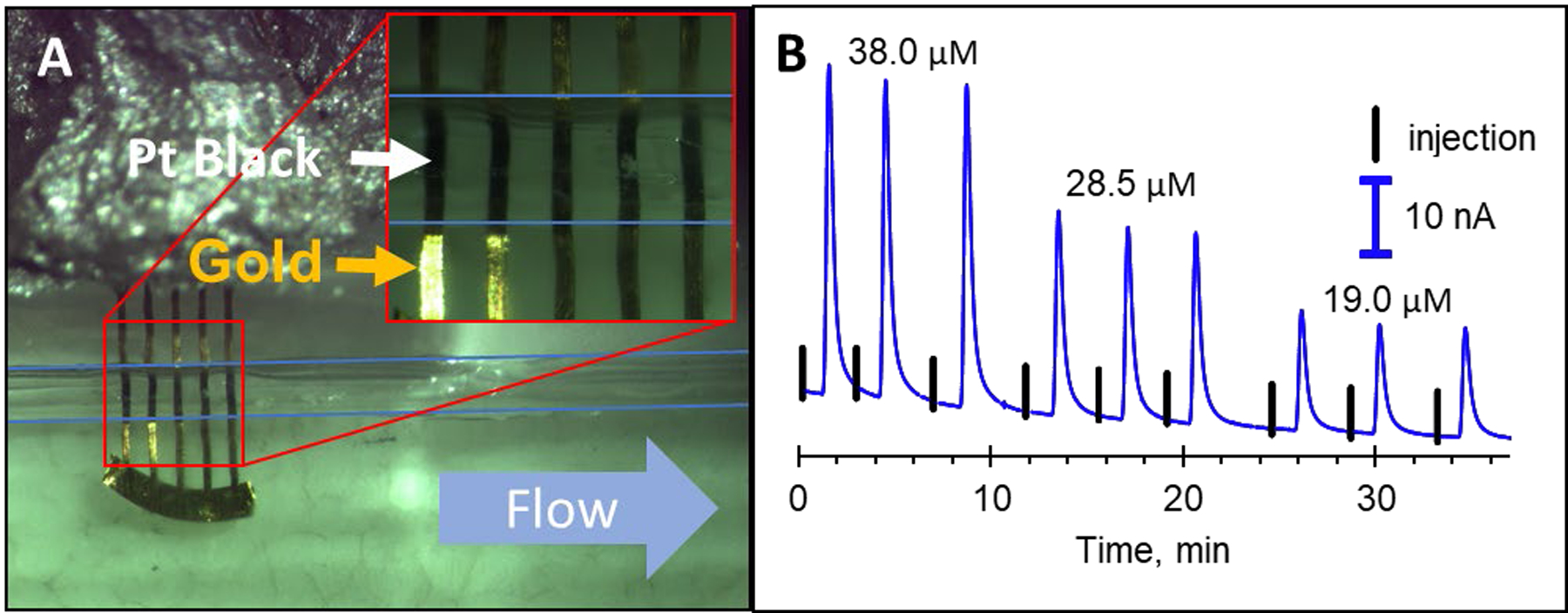
In situ platinum black deposition on the electrode array for the detection of nitric oxide. (A) Optical image of the electrode array after platinum black deposition. Black uniform coatings can clearly be seen on the electrode portion in the channel. (B) Triplicate injections of 38.0, 28.5, and 19.0 μM nitric oxide as detected on a platinum black-coated gold array placed in the middle of the channel. The black lines show where the injections were made.
An exciting feature of this stacked printing approach is the ability to place electrodes anywhere in the channel. This includes multiple electrodes in the same plane and multiple electrode materials for various functions (such as a counter electrode). To illustrate the effectiveness and versatility of this approach, a generator-collector electrode configuration was fabricated and tested.31 The designs discussed above relied on external reference (Ag/AgCl) and counter (Pt) electrodes placed in a reservoir downstream of the gold working electrodes, however, this device incorporated a single counter/quasi-reference electrode (Pt foil) embedded at the bottom of the channel (opposite with the dual gold working electrodes that were embedded in the middle of the channel). Figure 6A shows a schematic representation of a side view of the device configuration. There was still a capillary embedded to facilitate fluidic connections. A section of Pt foil (5 × 3 mm, 0.025 mm in thickness) was cut and embedded at the bottom of the channel (shown in gray), such that the exposed area in the channel was 3 mm × 376 μm (channel width). As can be seen in Figure 6, the two gold working electrode arrays (one acting as a generator, the other as a collector) were embedded in the center of the channel for optimal sensitivity. The fabrication process for this device was more involved, requiring four models to be stacked on top of each other during the printing process (Figure 6B) to form the final device. Even with this added complexity, three devices can be fabricated in less than 90 minutes. This includes approximately 60 minutes of active interaction with the printer during the stacked printing process (where printing occurs along with placing the electrodes/capillary and re-setting tray positions) and 30 minutes of printing without interaction (time to print the cover model). To further simplify the fabrication process, flat style alligator clamps were used to make connections with each electrode (one to each of the working electrodes and one to the counter electrode, see Figure 6C). This means that the device can be immediately removed from the print tray, flushed with IPA (to remove liquid support), and then used immediately for experiments. For this generator-collector experiment, the distance between the two working electrodes was set to ~750 μm, from the last post in the oxidation array to the first post in the reduction array. Figure 6D shows the amperometric trace for the oxidation (+800 mV vs Pt) of catechol and subsequent reduction of the quinone (−250 mV vs Pt). This design resulted in a 20% collection efficiency, which is comparable to other work including a PDMS-based microchip electrophoresis dual electrode detector (collection efficiencies ranged from 25–29%)7 and a HPLC-dual electrode flow cell (collection efficiencies ranged from 17%−38%).31
Figure 6.
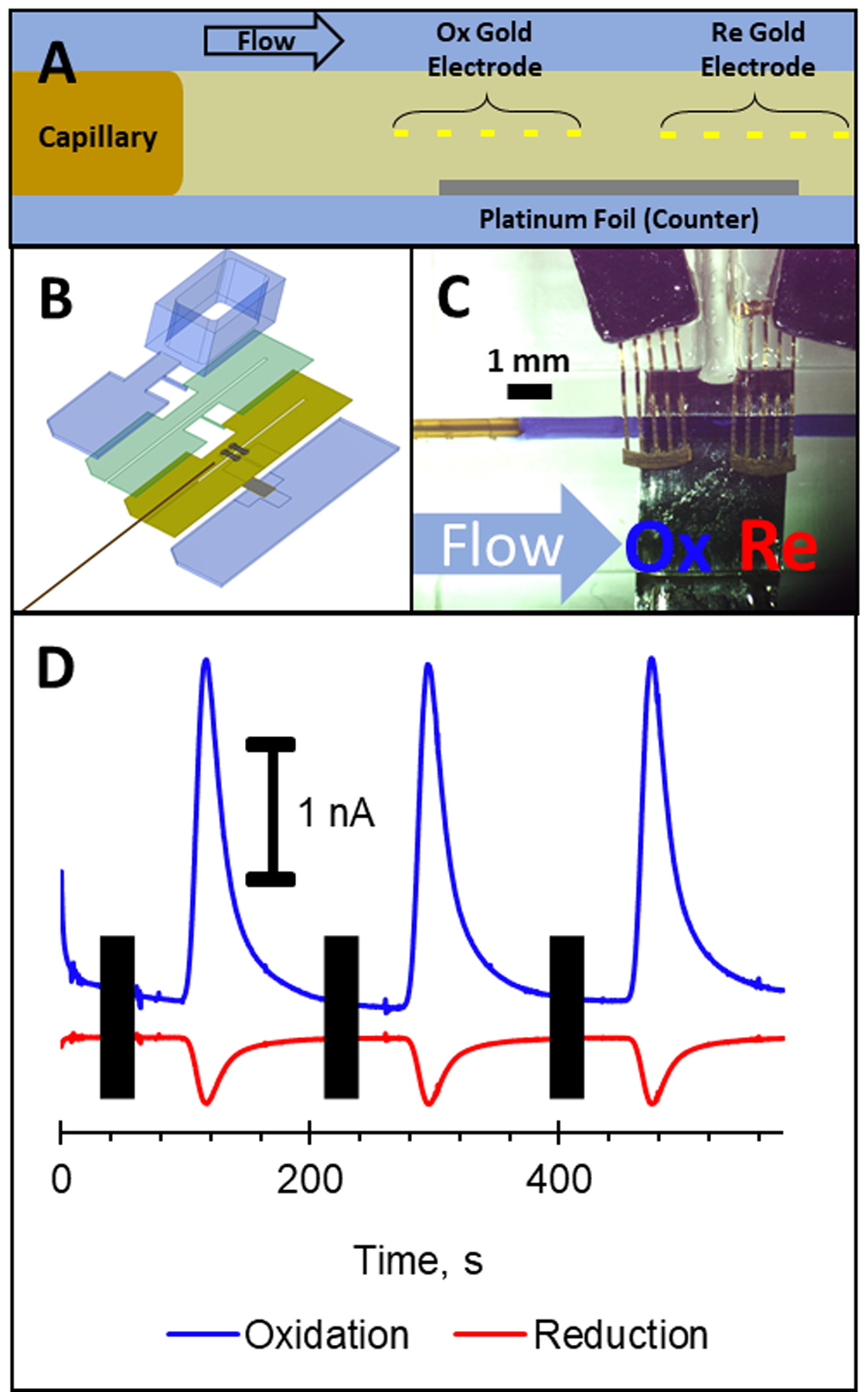
Embedded dual working electrode arrays with platinum counter electrode. (A) Schematic showing electrode placement (channel side view) with the two working electrode arrays in the middle of the channel and the platinum counter electrode at the bottom of the channel. (B) Exploded CAD rendering of the fabrication design process entailing stacking of three models on top of the base layer. (C) Optical image showing the working electrode arrays separated by ~750 μm, with the platinum counter electrode (3 mm wide) being placed 188 μm below the array. The channel is filled with trypan blue to help visualization. (D) Amperometric trace showing oxidation (+800 mV) of catechol (10 μM) and subsequent reduction (−250 mV) of the oxidized product (quinone).
Conclusion
A new method for the total integration of electrochemical detectors in microfluidic systems has been reported. This approach results in electrodes that can be placed at various points in the microchannel, as desired. This can be done with a single electrode or an electrode array (which led to increases in signal) as well as fused silica capillary (for fluidic connections). It was shown that a middle electrode configuration leads to a significant increase in the sensitivity, as opposed to more traditional thin-layer or bottom channel placement. Since the electrode is embedded in the device, in situ platinum black deposition was performed to aid in the detection of nitric oxide, with a LOD of 45 nM being possible. Finally, a generator-collector configuration with an opposed counter electrode was made by placing two working electrodes ~750 μm apart suspended in the middle of the channel. This embedding approach not only affords robust electrochemical detection schemes with new electrode configurations being possible (in a manner where any researcher can have access to the files for reproduction) but also opens up exciting new areas of embedding other functions into 3D printed devices (such as cell scaffolds for 3D culture and fiber optics).
Supplementary Material
Acknowledgments
The authors would like to acknowledge Prof. Sara McBride-Gagyi (Department of Orthopedic Surgery at Saint Louis University) for assisting with the microCT scans. The authors would also like to acknowledge Saint Louis University’s Center for Additive Manufacturing (SLU-CAM) and the Parks College of Engineering, Aviation and Technology for maintaining and providing access to the Eden 260V 3D printer. The work was funded by the National Institutes of Health (2R15GM084470-05A1).
References
- 1.Wang J, Electroanalysis, 2005, 17, 1133–1140. [Google Scholar]
- 2.Zhang Y and Ozdemir P, Anal Chim Acta, 2009, 638, 115–125. [DOI] [PubMed] [Google Scholar]
- 3.Samiei E, Tabrizian M and Hoorfar M, Lab Chip, 2016, 16, 2376–2396. [DOI] [PubMed] [Google Scholar]
- 4.Sonker M, Sahore V and Woolley AT, Anal Chim Acta, 2017, 986, 1–11. [DOI] [PMC free article] [PubMed] [Google Scholar]
- 5.Erkal JL, Selimovic A, Gross BC, Lockwood SY, Walton EL, McNamara S, Martin RS and Spence DM, Lab Chip, 2014, 14, 2023–2032. [DOI] [PMC free article] [PubMed] [Google Scholar]
- 6.Lacher NA, Lunte SM and Martin RS, Anal Chem, 2004, 76, 2482–2491. [DOI] [PubMed] [Google Scholar]
- 7.Martin RS, Gawron AJ and Lunte SM, Anal Chem, 2000, 72, 3196–3202. [DOI] [PubMed] [Google Scholar]
- 8.Munshi AS and Martin RS, Analyst, 2016, 141, 862–869. [DOI] [PMC free article] [PubMed] [Google Scholar]
- 9.Rowe AA, Bonham AJ, White RJ, Zimmer MP, Yadgar RJ, Hobza TM, Honea JW, Ben-Yaacov I and Plaxco KW, PLoS One, 2011, 6, e23783. [DOI] [PMC free article] [PubMed] [Google Scholar]
- 10.Ainla A, Mousavi MPS, Tsaloglou MN, Redston J, Bell JG, Fernandez-Abedul MT and Whitesides GM, Anal Chem, 2018, 90, 6240–6246. [DOI] [PMC free article] [PubMed] [Google Scholar]
- 11.Adams SD, Doeven EH, Quayle K and Kouzani AZ, Ieee Access, 2019, 7, 31903–31912. [Google Scholar]
- 12.Woolley AT, Lao K, Glazer AN and Mathies RA, Anal Chem, 1998, 70, 684–688. [DOI] [PubMed] [Google Scholar]
- 13.Wang J, Talanta, 2002, 56, 223–231. [DOI] [PubMed] [Google Scholar]
- 14.Chatzimichail S, Supramaniam P, Ces O and Salehi-Reyhani A, Sci Rep, 2018, 8, 14380. [DOI] [PMC free article] [PubMed] [Google Scholar]
- 15.Saem S, Zhu Y, Luu H and Moran-Mirabal J, Sensors, 2017, 17. [DOI] [PMC free article] [PubMed] [Google Scholar]
- 16.Nantaphol S, Channon RB, Kondo T, Siangproh W, Chailapakul O and Henry CS, Anal Chem, 2017, 89, 4100–4107. [DOI] [PubMed] [Google Scholar]
- 17.Martin RS, Gawron AJ, Fogarty BA, Regan FB, Dempsey E and Lunte SM, Analyst, 2001, 126, 277–280. [DOI] [PubMed] [Google Scholar]
- 18.Duffy DC, McDonald JC, Schueller OJA and Whitesides GM, Analytical Chemistry, 1998, 70, 4974–4984. [DOI] [PubMed] [Google Scholar]
- 19.Johnson AS, Mehl BT and Martin RS, Anal Methods, 2015, 7, 884–893. [DOI] [PMC free article] [PubMed] [Google Scholar]
- 20.Mehl BT and Martin RS, Anal. Methods, 2019, 11, 1064–1072. [DOI] [PMC free article] [PubMed] [Google Scholar]
- 21.Anderson KB, Lockwood SY, Martin RS and Spence DM, Anal Chem, 2013, 85, 5622–5626. [DOI] [PubMed] [Google Scholar]
- 22.Chen C, Mehl BT, Munshi AS, Townsend AD, Spence DM and Martin RS, Anal Methods, 2016, 8, 6005–6012. [DOI] [PMC free article] [PubMed] [Google Scholar]
- 23.Bishop GW, Satterwhite-Warden JE, Bist I, Chen E and Rusling JF, ACS Sens, 2016, 1, 197–202. [DOI] [PMC free article] [PubMed] [Google Scholar]
- 24.Molina DE, Medina AS, Beyenal H and Ivory CF, J Electrochem Soc, 2019, 166, B125–B132. [DOI] [PMC free article] [PubMed] [Google Scholar]
- 25.Duarte LC, Chagas CLS, Ribeiro LEB and Coltro WKT, Sens Actuators B Chem, 2017, 251, 427–432. [Google Scholar]
- 26.O’Neil GD, Ahmed S, Halloran K, Janusz JN, Rodríguez A and Terrero Rodríguez IM, Electrochem, 2019, 99, 56–60. [Google Scholar]
- 27.Li F, Macdonald NP, Guijt RM and Breadmore MC, Lab Chip, 2018, 19, 35–49. [DOI] [PubMed] [Google Scholar]
- 28.Castiaux AD, Pinger CW, Hayter EA, Bunn ME, Martin RS and Spence DM, Anal Chem, 2019, 91, 6910–6917. [DOI] [PMC free article] [PubMed] [Google Scholar]
- 29.Liu Y, Vickers JA and Henry CS, Anal Chem, 2004, 76, 1513–1517. [DOI] [PubMed] [Google Scholar]
- 30.Lunte CE, Kissinger PT and Shoup RE, Anal Chem, 1985, 57, 1541–1546. [Google Scholar]
- 31.Roston DA and Kissinger PT, Anal Chem, 1982, 54, 429–434. [Google Scholar]
- 32.Amatore C, Da Mota N, Lemmer C, Pebay C, Sella C and Thouin L, Anal Chem, 2008, 80, 9483–9490. [DOI] [PubMed] [Google Scholar]
- 33.Pluangklang T, Wydallis JB, Cate DM, Nacapricha D and Henry CS, Anal Methods, 2014, 6, 8180–8186. [DOI] [PMC free article] [PubMed] [Google Scholar]
- 34.Selimovic A, Johnson AS, Kiss IZ and Martin RS, Electrophoresis, 2011, 32, 822–831. [DOI] [PMC free article] [PubMed] [Google Scholar]
- 35.Selimovic A and Martin RS, Electrophoresis, 2013, 34, 2092–2100. [DOI] [PMC free article] [PubMed] [Google Scholar]
- 36.Bhattacharjee N, Urrios A, Kang S and Folch A, Lab Chip, 2016, 16, 1720–1742. [DOI] [PMC free article] [PubMed] [Google Scholar]
- 37.Li Y, Sella C, Lemaître F, Guille-Collignon M, Thouin L and Amatore C, Electrochimica Acta, 2014, 144, 111–118. [Google Scholar]
Associated Data
This section collects any data citations, data availability statements, or supplementary materials included in this article.


